

Page 1

HT9032
Calling Line Identification Receiver
1 April 6, 2000
Features
·
HT9032B/C/D operating voltage: 3.5V~5.5V
HT9032F operating voltage: 3.0V~5.5V
·
Bell 202 FSK and V.23 demodulation
·
Ring detection input and output
·
Carrier detection output
·
Power down mode
·
High input sensitivity
·
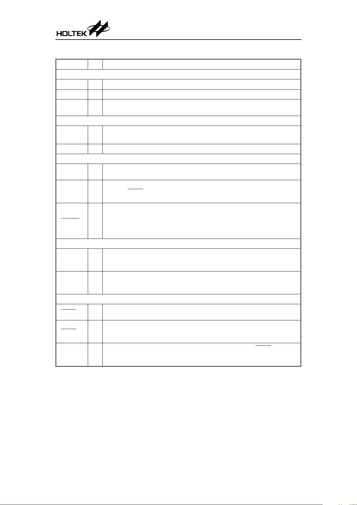
HT9032C: 16-pin DIP/SOP package
HT9032B/F-A: 8-pin DIP package
HT9032D/F-B: 8-pin SOP package
Applications
·
Feature phones
·
Caller ID adjunct boxes
·
Fax and answering machines
·
Computer telephony interface products
·
ADSI products
General Description
The HT9032 calling line identification receiver
is a low power CMOS integrated circuit de
signed for receiving physical layer signals transmitted according to Bellcore TR-NWT-000030
and ITU-T V.23 specifications. The primary ap
plication of this device is for products used to
receive and display the calling number, or mes
sage waiting indicator sent to subscribers from
the central office facilities. The device also pro
vides a carrier detection circuit and a ring de
tection circuit for easier system applications.
Page 2
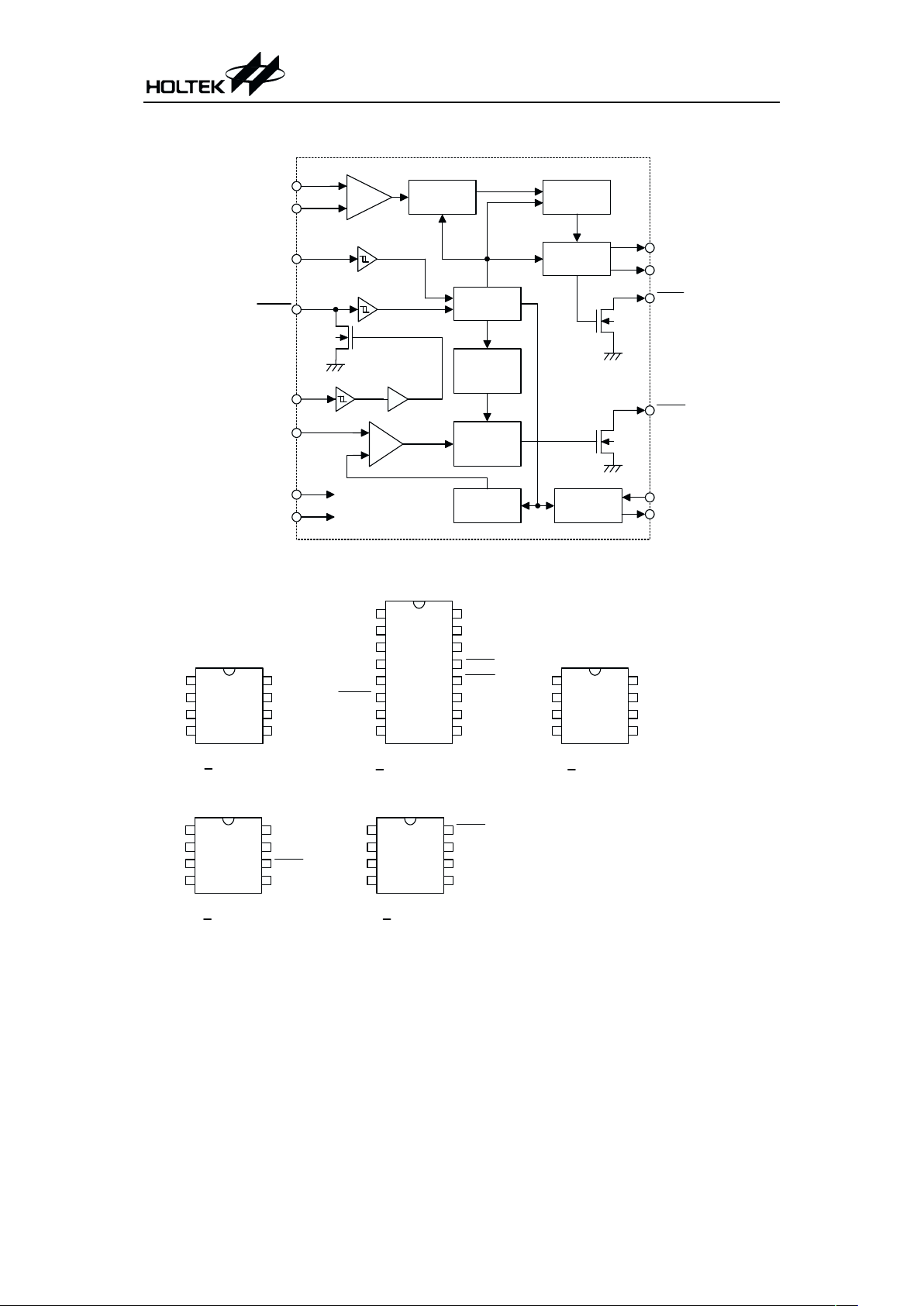
Block Diagram
Pin Assignment
HT9032
2 April 6, 2000
Band Pass
F ilte r
Power Up
Logic
D em odulator
Valid Data
Detection
DOUTC
DOUT
Internal
Power Up
Logic
Ring
Analysis
Circuit
R eference
Voltage
Clock
G enerator
CDET
RDET
VSS
VDD
RDET2
TIP
RING
PDW N
RTIM E
RDET1
X1
X2
H T9032B
8 D IP
TIP
PDW N
RING
VSS
X2
DOUT
X1
NC
NC
TIP
VDD
RTIM E
RDET1
X2
PDW N
VSS
RING
CDET
RDET
X1
RDET2
DOUTC
DOUT
H T9032C
16 D IP /S O P
VDD
1
2
3
4
8
7
6
5
1
2
3
4
5
6
7
8
16
15
14
13
12
11
10
9
H T9032D
8 S O P
DOUT
TIP
VDD
RING
PDW N
X2
VSS
X1
1
2
3
4
8
7
6
5
H T9032F-A
8 D IP
TIP
PDW N
RING
VSS
X1
DOUT
CDET
VDD
1
2
3
4
8
7
6
5
H T9032F-B
8 S O P
DOUT
TIP
VDD
RING
PDW N
X1
VSS
CDET
1
2
3
4
8
7
6
5
Page 3
Pin Description
Pin Name I/O Description
Power Inputs
VDD
¾
Power-VDD is the input power for the internal logic.
VSS
¾
Ground-VSS is ground connection for the internal logic.
PDWN I
A logic ²1² on this pin puts the chip in power down mode. When a logic ²0² is on
this pin, the chip is activated. This is a schmitt trigger input.
Clock
X1 I
A crystal or ceramic resonator should be connected to this pin and X2.
This pin may be driven from an external clock source.
X2 O A crystal or ceramic resonator should be connected to this pin and X1.
Ring Detections
RDET1 I
It detects ring energy on the line through an attenuating network and enables
the oscillator and ring detection. This is a schmitt trigger input.
RDET2 I
It couples the ring signal to the precision ring detector through an attenuating
network. RDET
=²0² if a valid ring signal is detected. This is a schmitt trigger in
-
put.
RTIME
I/O
An RC network may be connected to this pin in order to hold the pin voltage be
low 2.2V between the peaks of the ringing signal. This pin controls internal
power up and activates the partial circuitry needed to determine whether the
incoming ring is valid or not. The input is a schmitt trigger input. The output
cell structure is an NMOS output.
FSK Signal Inputs
TIP I
This input pin is connected to the tip side of the twisted pair wires. It is internally biased to 1/2 V
DD
when the device is in power up mode. This pin must be
DC isolated from the line.
RING I
This input pin is connected to the ring side of the twisted pair wires. It is internally biased to 1/2 V
DD
when the device is in power up mode. This pin must be
DC isolated from the line.
Detection Results
RDET
O
This open drain output goes low when a valid ringing signal is detected. When
connected to PDWN pin, this pin can be used for auto power up.
CDET
O
This open drain output goes low indicating that a valid carrier is present on the
line. A hysteresis is built-in to allow for a momentary drop out of the carrier.
When connected to PDWN pin, this pin can be used for auto power up.
DOUT O
This pin presents the output of the demodulator whenever CDET
pin is low.
This data stream includes the alternate ²1² and ²0² pattern, the marking, and
the data. At all other times, this pin is held high.
HT9032
3 April 6, 2000
Page 4

Pin Name I/O Description
DOUTC O
This output presents the output of the demodulator whenever CDET
pin is low
and when an internal validation sequence has been successfully passed. This
data stream does not include the alternate ²1² and ²0² pattern. This pin is al
-
ways held high.
Absolute Maximum Ratings
Voltages are referenced to VSS, except where noted.
Supply Voltage..............................-0.5V to 6.0V All Input Voltages ....................................25mW
Operating Temperature Range .......0°Cto70°C
Storage Temperature Range .....-40°Cto150°C
Note: These are stress ratings only. Stresses exceeding the range specified under ²Absolute Maxi
mum Ratings² may cause substantial damage to the device. Functional operation of this device
at other conditions beyond those listed in the specification is not implied and prolonged expo
sure to extreme conditions may affect device reliability.
D.C. Characteristics
Crystal=3.58MHz, Ta=0~70°C
Symbol Parameter
Test Conditions
Min. Typ. Max. Unit
V
DD
Conditions
V
DD
Supply Voltage
¾
9032B/C/D 3.5 5 5.5 V
9032F 3.0 5 5.5 V
I
DD1
Supply Current 5V PDWN=0 (3.58MHz OSC on)
¾
3.2 5 mA
I
DD2
Supply Current 5V
PDWN=1 and RTIME
=0
(3.58MHz OSC on and
internal circuits
partially on)
¾
1.9 2.5 mA
I
STBY
Standby Current 5V
PDWN=1 and RTIME
=1
(3.58MHz OSC off)
¾¾
1
mA
V
IL
Input Voltage Logic 0 5V
¾¾¾
0.2V
V
DD
V
IH
Input Voltage Logic 1 5V
¾
0.8V
¾¾
V
DD
I
OL
Output Voltage Logic 0 5V
I
OL
=1.6mA
¾
0.1V
V
DD
I
OH
Output Voltage Logic 1 5V
I
OH
=0.8mA
0.9V
¾¾
V
DD
I
IN
Input Leakage Current,
All Inputs
5V
¾-1 ¾
1
mA
V
T-
Input Low Threshold
Voltage
5V RDET1, RTIME
, PDWN 2.0 2.3 2.6 V
HT9032
4 April 6, 2000
Page 5

Symbol Parameter
Test Conditions
Min. Typ. Max. Unit
V
DD
Conditions
V
T+
Input High Threshold
Voltage
5V RDET1, RTIME
, PDWN 2.5 2.75 3.0 V
V
TRDET2
Input Threshold Voltage 5V RDET2 1.0 1.1 1.2 V
R
IN
Input DC Resistance 5V TIP, RING
¾
500
¾ kW
HT9032
5 April 6, 2000
TIP
VDD
RTIM E
RDET1
X2
PDW N
VSS
RING
CDET
RDET
X1
RDET2
DOUTC
DOUT
H T9032C
~
3.58M H z
10M
W
30pF
0.1mF
Supply current testing: All, except P D W N and R TIM E,
u n w ire d p in s a re le ft flo a tin g .
Page 6

A.C. Characteristics - FSK Detection
VSS=0V, Crystal=3.58MHz, Ta=0 to 70°C, 0dBm=0.7746Vrms @ 600W
Symbol Parameter
Test Conditions
Min. Typ. Max. Unit
V
DD
Conditions
Input Sensitivity: TIP,
RING
5V
-40 -45 ¾
dBm
S/N Signal to Noise Ratio 5V
¾
20
¾
dB
Band Pass Filter
60Hz
550Hz
2700Hz
3300Hz
5V
Frequency Response
Relative to 1700Hz @
0dBm
¾
-64
-4
-3
-34
¾
dB
Carrier Detect Sensitivity 5V
¾-48 ¾
dBm
t
DOSC
Oscillator Start Up Time 5V
¾¾2¾
ms
t
SUPD
Power Up to FSK Signal
Set Up Time
5V
¾
15
¾¾
ms
t
DAQ
Carrier Detect
Acquisition Time
5V
¾¾14¾
ms
t
DCH
End of Data to Carrier
Detect High
5V
¾
8
¾¾
ms
HT9032
6 April 6, 2000
R ing Signal
RTIM E
RDET
PDW N
CDET
DOUT
X1
010101..
DATA
2 Sec
3.58M H z
Raw DATA
t
DOSC
t
DAQ
t
SUPD
t
DCH
DOUTC
C ooked D A TA
1
0.5 Sec
0.5 Sec
Page 7

HT9032
7 April 6, 2000
Functional Description
The HT9032 is designed to be the physical layer
demodulator for products targeted for the caller
ID market. The data signaling interface should
conform to Bell 202, which is described as fol
-
lows:
·
Analog, phase coherent, frequency shift keying
·
Logical 1 (Mark)=1200+/-12Hz
·
Logical 0 (Space)=2200+/-22Hz
·
Transmission rate=1200bps
·
Data application=serial, binary,
asynchronous
The interface should be arranged to allow sim
ple data transmission from the terminating
central office, to the CPE (Customer Premises
Equipment), only when the CPE is in an
on-hook state. The data will be transmitted in
the silent period between the first and second
power ring before a voice path is established.
The transmission level from the terminating
C.O. will be -13.5dBm+/-1.0. The worst case at
tenuation through the loop is expected to be
-20dB. The receiver therefore, should have a
sensitivity of approximately -34.5dBm to han
dle the worst case installations. The ITU-T V.23
is also using the FSK signaling scheme to
transmit data in the general switched telephone network. For mode 2 of the V.23, the
modulation rate and characteristic frequencies
are listed below:
·
Analog, phase coherent, frequency shift keying
·
Logical 1 (Mark)=1300Hz
·
Logical 0 (Space)=2100Hz
·
Transmission rate=1200bps
Since the band pass filter of the HT9032 can
pass the V.23 signal, hence the HT9032 also can
demodulate the V.23 signal.
Ring detection
The data will be transmitted in the silent pe
-
riod between the first and second power ring be
fore a voice path is established. The HT9032
should first detect a valid ring and then per
form the FSK demodulation. The typical ring
detection circuit of the HT9032 is depicted be
low. The power ring signal is first rectified
through a bridge circuit and then sent to a re
sistor network that attenuates the incoming
power ring. The values of resistors and capaci
tor given in the figure have been chosen to pro
vide a sufficient voltage at RDET1 pin to turn
on the Schmitt Trigger input with approxi
mately a 40 Vrms or greater power ring input
from tip and ring. When V
T+
of the Schmitt is
exceeded, the NMOS on the pin RTIME
will be
driven to saturation discharging capacitor on
RTIME
. This will initialize a partial power up,
with only the portions of the part involved with
the ring signal analysis enabled, including
RDET2 pin. With RDET2 pin enabled, a portion
of the power ring above 1.2V is fed to the ring
analysis circuit. Once the ring signal is qualified, the RDET
pin will be sent low.
Power Up
Logic
Internal
Power Up
Logic
Ring
Analysis
Circuit
1.2V
RDET2
RDET
RTIM E
V
DD
0.2mF
270k
W
PDW N
RDET1
470k
W
18k
W
15k
W
To
Bridge
Page 8

Application Circuits
Application circuit 1
HT9032
8 April 6, 2000
Operation mode
There are three operation modes of the HT9032. They are power down mode, partial power up mode,
and power up mode. The three modes are classified by the following conditions:
Modes Conditions
Current
Consumption
Power down
PDWN=²1² and RTIME
=²1² <1mA
Partial power up
PDWN=²1² and RTIME
=²0²
1.9mA typically
Power up
PDWN=²0²
3.2mA typically
Normally, the PDWN pin and the RTIME pin
control the operation mode of the HT9032.
When both pins are HIGH, the HT9032 is set at
the power down mode, consuming less than 1mA
of supply current. When a valid power ring ar
-
rives, the RTIME pin will be driven below V
T-
and the portions of the part involved in the ring
signal analysis are enabled. This is partial
power up mode, consuming approximately
1.9mA typically. Once the PDWN pin is below
V
T-
, the part will be fully powered up, and ready
to receive FSK. During this mode, the device
current will increase to approximately 3.2mA
(typ). The state of the RTIME
pin is now a
²don¢t care² as far as the part is concerned. Af
ter the FSK message has been received, the
PDWN pin can be allowed to return to V
DD
and
the part will return to the power down mode.
H T 1050
~
~
TIP
VDD
X2
PDW N
VSS
RING
X1
DOUT
H T 9032B /D
3.58M H z
10M
W
30pF30pF
15k
W
18k
W
200k
W
0.01mF
470k
W
0.01mF200k
W
0.2mF
TIP
RING
0.2mF
0.1mF
9V
V
DD
m
C
Page 9

Application circuit 2
Application circuit 3
HT9032
9 April 6, 2000
H T 1050
~
~
TIP
VDD
RTIM E
RDET1
X2
PDW N
VSS
RING
CDET
RDET
X1
RDET2
DOUTC
DOUT
H T 9032C
20kW20k
W
3.58M H z
10M
W
30pF30pF
V
DD
270k
W
0.2mF
15k
W
18k
W
200k
W
0.01mF
470k
W
0.01mF200k
W
0.2mF
TIP
RING
0.2mF
0.1mF
9V
V
DD
m
C
H T 1050
~
~
TIP
VDD
PDW N
VSS
RING
X1
DOUT
H T 9032F
3.58M H z
10M
W
30pF30pF
15k
W
18k
W
200k
W
0.01mF
470k
W
0.01mF200k
W
0.2mF
TIP
RING
0.2mF
0.1mF
9V
V
DD
m
C
CDET
20k
W
Page 10

HT9032
10 April 6, 2000
Copyright ã 2000 by HOLTEK SEMICONDUCTOR INC.
The information appearing in this Data Sheet is believed to be accurate at the time of publication. However, Holtek
assumes no responsibility arising from the use of the specifications described. The applications mentioned herein are
used solely for the purpose of illustration and Holtek makes no warranty or representation that such applications
will be suitable without further modification, nor recommends the use of its products for application that may pres
ent a risk to human life due to malfunction or otherwise. Holtek reserves the right to alter its products without prior
notification. For the most up-to-date information, please visit our web site at http://www.holtek.com.tw.
Holtek Semiconductor Inc. (Headquarters)
No.3 Creation Rd. II, Science-based Industrial Park, Hsinchu, Taiwan, R.O.C.
Tel: 886-3-563-1999
Fax: 886-3-563-1189
Holtek Semiconductor Inc. (Taipei Office)
5F, No.576, Sec.7 Chung Hsiao E. Rd., Taipei, Taiwan, R.O.C.
Tel: 886-2-2782-9635
Fax: 886-2-2782-9636
Fax: 886-2-2782-7128 (International sales hotline)
Holtek Semiconductor (Hong Kong) Ltd.
RM.711, Tower 2, Cheung Sha Wan Plaza, 833 Cheung Sha Wan Rd., Kowloon, Hong Kong
Tel: 852-2-745-8288
Fax: 852-2-742-8657
 Loading...