

Page 1
HT9011
Preliminary
Features
Operating voltage: 1.1V~3.5V
·
Constant power supply voltage can be gen
·
erated by externally adding a transistor:
V
=1.0V typ.
REG
Alarm function sensitivity: V
·
Low current consumption: I
·
Built-in 2nd stage mixer for double conver
·
sion method
Mixer operating frequency: 10MHz~50MHz
·
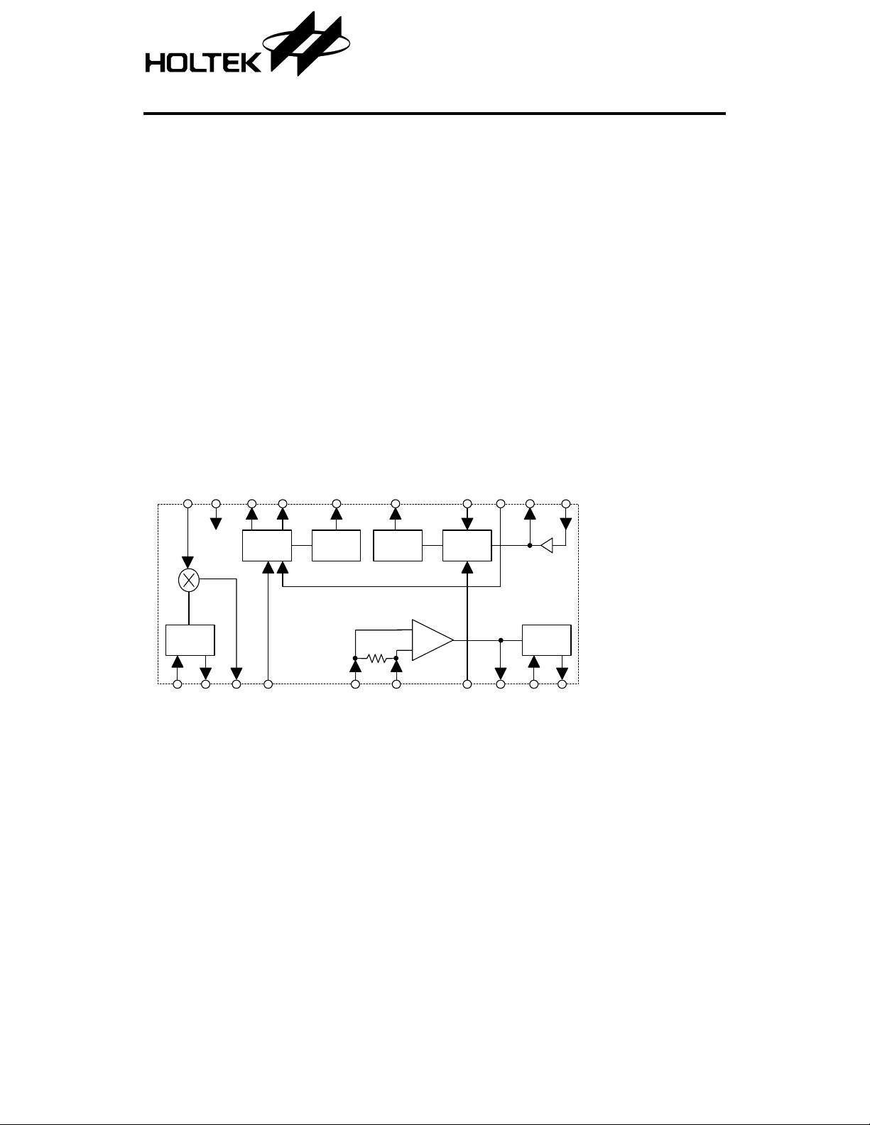
General Description
The HT9011 is designed for FM communication
system devices. It combines a paging system,
mixer, IF limiter, Quadrature detector, opera
tion amplifier, comparator and more. The
Block Diagram
MIXI
REGCGND REGO ALM FSKO CHG LPFOBS
=1.1V typ.
ALM
=1.1mA typ.
CCQ
FM IF Detector
Built-in low-pass filter and waveform shap
·
-
-
-
ing circuit enable the extraction of FSK sig
nals from voice signals
Built-in battery-saving function for longer
·
battery life time
High transmission rate: 1200 bps
·
20-pin SSOP package (0.65mm Pitch)
·
HT9011 could provide the customer¢s PAGER
system with total solution along with Holtek¢s
POCSAG Pager Controller series products.
LPFI
-
-
Mixer
OSC
OSCOOSCI MIXO
REG. ALARM
VCC FSKR
FSK
COM P.
IF IN
Quick
C harge
IF A m p
1 March 1, 2000
AM P
Q uad D et
AFOQUADIF ODEC
Page 2

Pin Assignment
Preliminary
HT9011
OSCI
OSCO
MIXO
VCC
IF IN
DEC
FSKR
IF O
QUAD
AFO
1
2
3
4
5
6
7
8
9
10
MIXI
20
GND
19
REGO
18
REGC
17
ALM
16
FSKO
15
CHG
14
BS
13
LPFO
12
LPFI
11
H T 9011
2 0 S S O P
Pin Description
Pin No. Pin Name I/O Description
1 OSCI I
2 OSCO O
3 MIXO O
4 VCC
5 IFIN I Input terminal for IF Amp.
6 DEC I Bias Decoupling
7 FSKR I
8 IFO O
9 QUAD I
10 AFO O FM demodulator output pin
11 LPFI I Low Pass Filter Input pin
12 LPFO O Low Pass Filter Output pin
13 BS I
These pins are connected to the external parts of an oscillating
circuit.
Mixer output pin. Connect a 455kHz ceramic filter between this
pin and the IFIN pin.
Positive power supply
¾
Reference input of differential amplifier for waveform shaping.
Connect the capacitor externally.
IF Amplifier Output pin. Connect the discriminator through the coupling capacitor.
FM demodulator phase shift input pin connected to a quadrature
detector phase shifter.
Battery-saving Control pin
²H² Normal Operation
²L² Battery-saving
2 March 1, 2000
Page 3

Preliminary
Pin No. Pin Name I/O Description
Control pin for quick charge-discharge circuit.
14 CHG I
15 FSKO O FSK NRZ data output
16 ALM O
17 REGC O
18 REGO O
19 GND
20 MIXI I MIXER Input terminal
²H² turn on quick charge-discharge
²L² turn off quick charge-discharge
Output pin for Low Voltage Alarm
@1.1V, this pin becomes ²H² (@VCC) and can indicate dete
At V
CC
rioration of battery.
Control pin of external transistor for regulator of external power
supply.
Externally connect the PNP transistor
Output voltage monitoring pin of regulator for external power
supply.
Negative power supply, ground
¾
HT9011
Absolute Maximum Ratings
Power Supply Voltage............VCC-0.3V to 4.0V Power Dissipation..................................730mW
Operating Temperature range ........0°Cto45°C
Storage Temperature.................-55°Cto150°C
-
Note: These are stress ratings only. Stresses exceeding the range specified under ²Absolute Maxi-
mum Ratings² may cause substantial damage to the device. Functional operation of this device
at other conditions beyond those listed in the specification is not implied and prolonged exposure to extreme conditions may affect device reliability.
3 March 1, 2000
Page 4

Preliminary
HT9011
Electrical Characteristics
Ta=25°C, Unless oterwise specified, Fin(MIX)=21.7MHz, Fin(IF)=455kHz, F
Symbol Parameter
Iccq Quiescent Current 1.4V
Icco
Supply Current at
Battery Saving
Test Conditions
V
DD
1.4V
Conditions
Min. Typ. Max. Unit
¾
¾
GMV MIXER Conversion Gain 1.4V 9 12.5 16 dB
IP
R(MIX)in MIX Input Resistance 1.4V
R(IF)in IF Amp Input Resistance 1.4V
S/N1 Signal to Noise Ration 1 1.4V
S/N2 Signal to Noise Ration 2 1.4V
S/N3 Signal to Noise Ration 3 1.4V
Vi(LIM)1
Vi(LIM)2
V
OD
AMR AM Rejection Ratio 1.4V
DR FSK OUT Duty Ratio 1.4V
V
ALM
V
ALML
I
ALM
V
FSKL
I
FSK
V
REC
MIXER 3rd Interception
point
1.4V
¾-10 ¾
¾
¾
-3dB Limiting
Sensitivity 1
-3dB Limiting
Sensitivity 2
1.4V MIX input
1.4V IF input
Detected Output Level 1.4V
MIX IN,
(MIX)=60dBmEMF
V
IN
IF IN,
(IF)=60dBmEMF
V
IN
IF IN,
(IF)=22dBmEMF
V
IN
(IF)=60dBmEMF
V
IN
(IF)=60dBmEMF
V
IN
AM=30%
(IF)=60dBmEMF
V
IN
¾
¾
¾
¾
¾
30 45 60 mVrms
¾
40 50 60 %
Alarm Detected Voltage 1.4V 1.05 1.1 1.15 V
²L² Level Output Voltage
(ALM)
²H² Level Output Current
(ALM)
²L² Level Output Voltage
(FSK)
²H² Level Output Current
(FSK)
1.4V
I=100mA ¾¾
1.4V
1.4V
I=100mA ¾¾
1.4V
¾¾
¾¾
Constant Voltage Output 1.4V 0.95 1.0 1.05 V
=±4kHz, Fin=600Hz
dev
1.1 1.6 mA
05
5
¾ kW
2
¾ kW
63
¾
63
¾
25
¾
14
¾ dBmEMF
23 27
50
dBmEMF
¾
0.4 V
2
0.4 V
2
mA
dBm
dB
dB
dB
dB
mA
mA
4 March 1, 2000
Page 5
Preliminary
Functional Description
Battery-saving function
The battery-saving function is controlled by the
pin ²BS² and the battery consumption is mini
mized by reducing the current consumption. If
the pin is logic LOW, the HT9011 enters the
battery-saving mode, otherwise HT9011 is in
normal operation state.
Battery low alarm function
In case the HT9011 is battery powered, when
the power supply voltage goes low to about 1.1V,
the output of the pin ²ALM² rises up to about
1.1V and the battery voltage can be monitored
by other devices. The output is an open collector
similar to FSK NRZ output.
HT9011
FSK NRZ output
The HT9011 has two built-in operation amplifi
ers. One of these operation amplifiers is con
nected inside the IC to the NRZ comparator.
The NRZ comparator can output the input sig
nal waveform as a square wave. The NRZ com
parator output is an open collector. If the IC
interfaces with CMOS devices, the possible con
nection is shown below.
V
CC
1.5V
4
VCC fo r
CMOS IC
14
FSKO
CMOS IC
Quick charge-discharge circuit
If an FSK signal inputs during the brief transition from battery-saving state to normal operation state, the time that the pin ²FSKR² arrives
at the reference voltage is delayed by a time
constant determined by the capacitor connected
to the pin ²FSKR² and the internal resistor.
Sometimes, the output signal becomes errone
ous due to some error in the comparator input
voltage. Such a case could be avoided by quickly
charging or discharging the capacitor con
nected to the pin ²FSKR². By using the quick
charge-discharge circuit, the delay time for the
²FSKR² pin to be of the same level with the
²LPFO² pin could be minimized, hence, errone
ous FSK NRZ output signal is prevented.
Constant voltage regulator for external part
power supply
Externally connecting the transistor as shown
in the figure below, the output ²REGO² could be
-
used constantly as 1.0V regulator output. At
-
the battery-saving mode, the regulator is
turned OFF .
-
Vreg
V
+
2N 3906
1.0mF
REGO REGC
CC
Local oscillator circuit
The HT9011 local oscillator circuit is of Colpitts
type oscillator composed of internal emitter follower circuit and an external X¢tal. The transistor is connected externally as shown in the
figure below. Resistor ²R² may be needed to increase the current of the local oscillator circuit
in order to compose the overtone oscillator and
improve its stability. It is recommended that
the resistor be connected between OSCI and
REGO to provide battery-saving mode.
-
-
REGO
21.855M H z
OSCI OSCO
1 2
22k
W
56pF
47pF
-
R
5 March 1, 2000
Page 6

Application Circuits
Pager RF board (149.7MHz)
Preliminary
2pF
39pF
2~10pF
0.001mF
22pF
5pF
0.01mF
56k
W
3103331033
100
20pF
82mH
HT9011
W
12
W
2~10pF
12pF
560
0.001mF
680nH
3.9k
W
2.2k
10mF
4.7k
2pF
+
1.5V
W
0.1mF
120nH
W
9pF
B+
TP
21.855M H z
C FW M 455F
345
455C 28
3.3k
56pF
47pF
12
TP3
TP
0.1mF
10mF
22pF
W
22k
1
OSCI
2
OSCO
3
MIXO
4
VCC
5
IF IN
6
DEC
7
FSKR
+
8
IF O
9
QUAD
10
AFO
3pF
31033
W
NO
NO
39nH
6pF
W
H T9011
12k
20pF
TP
0.001mF
2734
MIXI
GND
REGO
REGC
ALM
FSKO
CHG
BS
LPF O
LPF I
56pF
0.1mF
W
0.01mF
TP1
0.01mF
47k
W
2.7mH
18k
W
0.001mF
20
19
18
17
16
10k
W
15
10k
W
14
47k
W
13
10k
W
12
11
68k
W
20pF
BAL
DATA
BS2
BS1
0.01mF
2N 3906
120
0.01mF
0.1mF
B+
W
0.1mF
68k
0.0033mF
68k
TP
TP3
W
W
6 March 1, 2000
Page 7

Preliminary
HT9011
Holtek Semiconductor Inc. (Headquarters)
No.3 Creation Rd. II, Science-based Industrial Park, Hsinchu, Taiwan, R.O.C.
Tel: 886-3-563-1999
Fax: 886-3-563-1189
Holtek Semiconductor Inc. (Taipei Office)
5F, No.576, Sec.7 Chung Hsiao E. Rd., Taipei, Taiwan, R.O.C.
Tel: 886-2-2782-9635
Fax: 886-2-2782-9636
Fax: 886-2-2782-7128 (International sales hotline)
Holtek Semiconductor (Hong Kong) Ltd.
RM.711, Tower 2, Cheung Sha Wan Plaza, 833 Cheung Sha Wan Rd., Kowloon, Hong Kong
Tel: 852-2-745-8288
Fax: 852-2-742-8657
Copyright ã 2000 by HOLTEK SEMICONDUCTOR INC.
The information appearing in this Data Sheet is believed to be accurate at the time of publication. However, Holtek
assumes no responsibility arising from the use of the specificationsdescribed. Theapplications mentionedherein are
used solely for the purpose of illustration and Holtek makes no warranty or representation that such applications
will be suitable without further modification, nor recommends the use of its products for application that may pres
ent a risk to human life due to malfunction or otherwise. Holtek reserves the right to alter its products without prior
notification. For the most up-to-date information, please visit our web site at http://www.holtek.com.tw.
7 March 1, 2000
-
 Loading...