

Page 1

Features
Operating voltage: 4.5V~5.5V
·
ADM algorithm
·
Low noise
·
-
Echo mode:-85dB
-
Surround mode:-90dB
Low distortion rate
·
-
Echo mode: 1%
-
Surround mode: 0.2%
Applications
Television
·
Karaoke systems
·
General Description
The HT8970 is an echo/surround effect processor.
It is designed for various audio systems including
karaoke, television, sound equipments, etc. The
chip consists of a built-in pre-amplifier, VCO or
Voltage Control OSC, 20Kb SRAM, A/D and D/A
converters as well as delay time control logic.
HT8970
Voice Echo
Built-in 20Kb SRAM
·
Automatic reset function
·
Package type: 16-pin DIP/SOP
·
Video disc player
·
Sound equipments
·
Its built-in 20Kb SRAM can generate delay
time effect and can control the delay time value
through the external VCO resistor.
The VCO circuit can reduce external compo
nents and make it easy to adjust the delay time.
-
1 March 14, 2000
Page 2
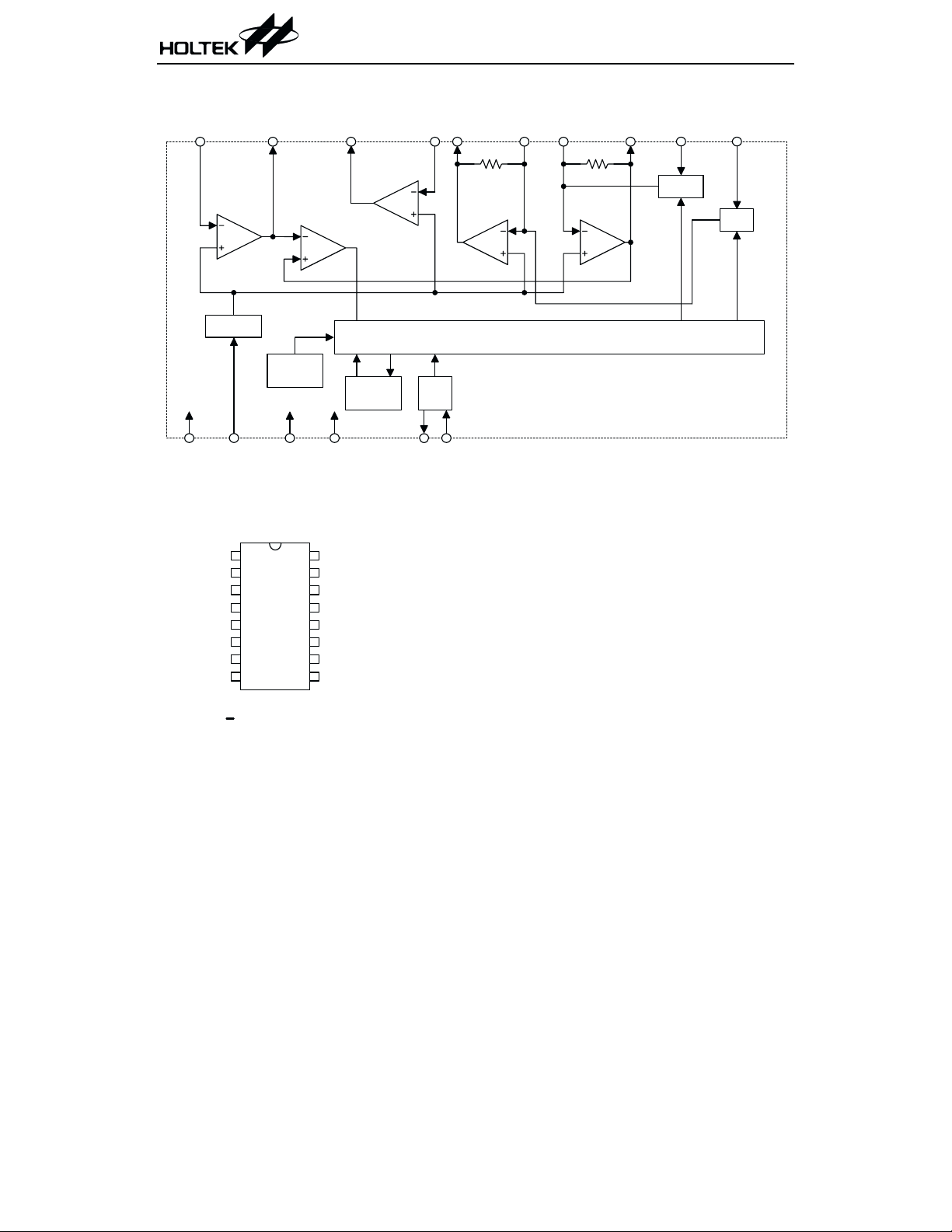
Block Diagram
LPF1_IN
LPF1_O U T LPF2_O U T LP F2_IN O P2_O U T O P 2_IN O P 1_IN O P 1_O U T C C 0 C C 1
4.7k
HT8970
4.7k
W
W
MOD
COM P
LPF1
1/2 V C C
AUTO
RESET
VCC AGND DGND
Pin Assignment
16
1
VCC
15
2
REF
14
VCO
CC1
CC0
H T 8 9 7 0
16 D IP /SO P
3
13
4
12
5
11
6
10
7
8
9
AGND
DGND
OSC_O
LPF2
DI
MO MI CLOCK
20K Bits
RAM
OSC_OREF
LPF1_IN
LPF1_O U T
LPF2_O U T
LPF2_IN
O P 2_O U T
O P 2_IN
O P 1_IN
O P 1_O U T
DEM
DO0 DO1
VCO
vco
2 March 14, 2000
Page 3
HT8970
Pad Assignment
* The IC substrate should be connected to VSS in the PCB layout artwork.
DGND
OSC_O
VCO
CC1
LPF2_O U T
LPF1_O U T
AGND
16
1
2
3
4 5
CC0
REF
15
6
O P1_O U T
VCC
14
(0 ,0 )
7
O P1_IN
LPF1_IN
13
12
8
O P2_IN
Chip size: 1790 ´ 2215 (mm)
LPF2_IN
10 11
9
O P2_O U T
2
Pad Coordinates
Pad No. X Y Pad No. X Y
1
-698.00
2
-669.25 -614.45
3
-669.25 -762.85
4
-669.25 -945.30
5
-405.55 -945.30
6
-140.05 -945.30
7 123.65
8 389.15
701.70 9 652.85
10 720.20 882.55
11 571.80 882.55
12 423.40 882.55
13 275.00 882.55
-945.30
-945.30
14
15
16
-77.60
-306.55
-560.95
3 March 14, 2000
Unit: mm
-945.30
877.60
849.95
737.70
Page 4

Pad Description
HT8970
Pad No. Pad Name I/O
1 DGND I
2 OSC_O O
3 VCO I
4 CC1
5 CC0
6 OP1_OUT O
7 OP1_IN I
8 OP2_IN I
9 OP2_OUT O
10 LPF2_IN I
11 LPF2_OUT O
12 LPF1_OUT O
13 LPF1_IN I
14 VCC I
15 REF I
16 AGND I
¾¾
¾¾
Internal
Connection
¾
¾
¾
¾
¾
¾
¾
¾
¾
¾
¾
¾
¾
¾
Description
Digital ground
System oscillator output
System oscillator input, system frequency
adjustable pin
Current control 1
Current control 0
OP1 output
OP1 input
OP2 input
OP2 output
Low pass filter 2 input
Low pass filter 2 output
Low pass filter 1 output
Low pass filter 1 input
Analog and positive power supply
Analog reference voltage
Analog ground
Absolute Maximum Ratings
Supply Voltage.................................-0.3V to 6V
Input Voltage .................V
Note: These are stress ratings only. Stresses exceeding the range specified under ²Absolute Maxi
mum Ratings² may cause substantial damage to the device. Functional operation of this device
at other conditions beyond those listed in the specification is not implied and prolonged expo
sure to extreme conditions may affect device reliability.
-0.3V to VDD+0.3V
SS
Storage Temperature.................-50°Cto125°C
Operating Temperature ..............-20°Cto70°C
4 March 14, 2000
-
-
Page 5

HT8970
Electrical Characteristics
Symbol Parameter
V
CC
I
CC
G
V
V
OMAX
Operating Voltage
Operating Current 5V
Voltage Gain 5V
Maximum Output Voltage 5V THD=10% 0.9 1.8
THD Total Harmonic Distortion 5V 30kHz L.P.F.
N
O
PSRR
Output Noise Voltage 5V DIN Audio
Power Supply Rejection
Ratio
Test Conditions
V
DD
Conditions
¾¾
¾¾
=47kW¾-0.9
R
L
=-20dBV
DV
5V
CC
(0.1Vrms)
f=100Hz
Functional Description
The HT8970 is an echo/surround effect genera
tor with built-in 20Kb SRAM. It ensures low
distortion as well as low noise for processing
audio signal delay. The chip provides two play
ing modes (echo and surround) and the playing
function block diagrams are shown as follows.
·
Surround mode
·
-
-
Echo mode
V
IN
V
LPF1 A/D
Ta=25°C
Min. Typ. Max. Unit
4.5 5.0 5.5 V
15 30 mA
2.5 dB
Vrms
¾
0.7 1.5 %
¾
¾-85 -60
¾-40 -30
OUT
Delay
D/A LPF2
dBV
dB
V
IN
LPF1 A /D
Delay
D/A LPF2
V
OUT
5 March 14, 2000
Page 6

HT8970
R
OSC-fOSC
-Delay_time-Distortion Cross table
R
f
OSC
OSC
49.8 38.3 31.9 26.77 23.3 20.54 18.08
2M 2.5M 3M 3.5M 4M 4.5nm 5M MHz
Td 327.6 262 218.4 187.2 163.8 145.6 131 ms
THD 1.6 1.3 1.0 0.72 0.7 0.64 0.5 %
R
f
OSC
OSC
16.07 14.29 12.98 11.97 11 9.99 9.22
5.5M 6M 6.5M 7M 7.5M 8M 8.5M MHz
Td 119.1 109.2 100.8 93.6 87.36 81.89 77.08 ms
THD 0.47 0.38 0.36 0.35 0.3 0.29 0.28 %
R
f
OSC
OSC
8.5 7.54 6.66 6.12 5.5 4.85 4.4
9M 10M 11M 12M 13M 14M 15M MHz
Td 72.79 65.52 59.56 54.59 50.39 46.79 43.68 ms
THD 0.25 0.245 0.23 0.22 0.19 0.185 0.165 %
R
f
OSC
OSC
3.98 3.64 3.26 2.92 2.69 2.48 2.28
16M 17M 18M 19M 20M 21M 22M MHz
Td 40.94 38.54 36.39 34.48 32.75 31.19 29.78 ms
THD 0.165 0.15 0.14 0.14 0.13 0.12 0.11 %
kW
kW
kW
kW
6 March 14, 2000
Page 7

Application Circuits
Echo mode
HT8970
MIC
0.68mF
1k
W
4.7k
W
9V
5V
0.1mF
0.1mF
20k
100mF
4.7mF
W
0.1mF
1mF
4.7k
W
4.7k
W
1
VCC
2
REF
3
AGND
4
DGND
5
OSC_O
R
6
VCO
7
CC1
8
CC0
47k
W
100mF
4.7k
W
LPF1_O U T
LPF2_O U T
OP2_OUT
OP1_OUT
1k
W
560
22mF
LPF1_IN
LPF2_IN
OP2_IN
OP1_IN
W
16
15
14
13
12
11
10
9
3
4558
2
5600pF
10k
560pF
12k
13k
15k
560pF
10k
15k
0.047mF
0.047mF
9V
8
1
4
47k
W
39pF
15k
W
W
W
0.033mF
W
W
W
4.7mF
10mF
W
560pF
4.7mF
4.7mF
20k
W
15k
W
100k
4.7k
W
10mF
W
O utput
H T8970
Note: : Analog ground, : Digital ground
7 March 14, 2000
Page 8

Surround mode
HT8970
MIC
0.68mF
1k
W
4.7k
W
9V
5V
0.1mF
0.1mF
20k
100mF
4.7mF
W
0.1mF
1mF
4.7k
W
4.7k
W
1
VCC
2
REF
3
AGND
4
DGND
5
OSC_O
R
6
VCO
7
CC1
8
CC0
47k
W
100mF
4.7k
W
LPF1_O U T
LPF2_O U T
OP2_OUT
OP1_OUT
1k
W
560
22mF
LPF1_IN
LPF2_IN
OP2_IN
OP1_IN
W
16
15
14
13
12
11
10
9
3
4558
2
5600pF
10k
560pF
12k
560pF
10k
15k
0.047mF
0.047mF
9V
8
1
4
47k
W
39pF
15k
W
W
15k
W
W
W
W
560pF
10mF
4.7mF
4.7mF
20k
W
100k
W
3k
W
O utput
Note:
H T8970
: Analog ground, : Digital ground
8 March 14, 2000
Page 9

HT8970
Holtek Semiconductor Inc. (Headquarters)
No.3 Creation Rd. II, Science-based Industrial Park, Hsinchu, Taiwan, R.O.C.
Tel: 886-3-563-1999
Fax: 886-3-563-1189
Holtek Semiconductor Inc. (Taipei Office)
5F, No.576, Sec.7 Chung Hsiao E. Rd., Taipei, Taiwan, R.O.C.
Tel: 886-2-2782-9635
Fax: 886-2-2782-9636
Fax: 886-2-2782-7128 (International sales hotline)
Holtek Semiconductor (Hong Kong) Ltd.
RM.711, Tower 2, Cheung Sha Wan Plaza, 833 Cheung Sha Wan Rd., Kowloon, Hong Kong
Tel: 852-2-745-8288
Fax: 852-2-742-8657
Copyright Ó 2000 by HOLTEK SEMICONDUCTOR INC.
The information appearing in this Data Sheet is believed to be accurate at the time of publication. However, Holtek
assumes no responsibility arising from the use of the specifications described.The applications mentioned herein are
used solely for the purpose of illustration and Holtek makes no warranty or representation that such applications
will be suitable without further modification, nor recommends the use of its products for application that may pres
ent a risk to human life due to malfunction or otherwise. Holtek reserves the right to alter its products without prior
notification. For the most up-to-date information, please visit our web site at http://www.holtek.com.tw.
9 March 14, 2000
-
 Loading...