

Page 1

Features
·
Complete Universal Serial Bus specs V1.0
compatibility
·
Serial Bus Interface Engine (SIE)
·
USB transceiver
·
Microsoft 3D Intelli mouse and IBM PS/2
mouse compatible
·
Supports three buttons (R, M, L) and three
axes (X, Y, Z) input
·
Z axis can support two kinds of scroller in
put (optomechanical and mechanical)
General Description
HT82M98A is a 3D mouse controller especially
designed for USB and PS/2 applications. The
HT82M98A can support the USB Standard Re
quest as well as HID Class Request version 1.0
draft 4. It is compatible with Microsoft Intelli
3D PS/2 mouse. The X/Y axis photo input with
built-in Holtek¢s special dynamic photo-input
resistor and Z axis can support two kinds of
HT82M98A
3D USB+PS2 Mouse
·
Single chip solution especially for USB
mouse function
·
Halt function and wake-up feature reduce
power consumption
·
Plug and Play functions
·
Minimal external components
·
6MHz crystal oscillator for system clock
·
18-pin DIP package
-
scroller input, namely; optomechanical and
mechanical. It requires minimal external com
ponents to implement 3D USB plus PS/2
mouse. It can be briefly described as a Holtek
8-bit mC with an on-chip USB interface logic.
The USB is specified by the Universal Serial
Bus Specification V1.0.
-
1 June 14, 2000
Page 2
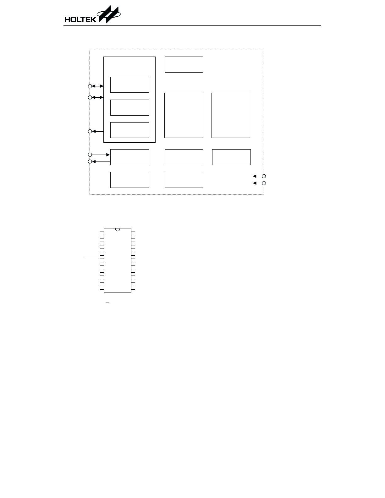
Block Diagram
HT82M98A
USBD+
USBD
-
V33O
OSC1
OSC2
Pin Assignment
VSS
1
V33O
USBD+/CLK
USBD-/D A T A
RESET
2
3
4
5
X1
6
X2
7
Y1
8
Y2
9
H T82M 98A
18 D IP
USB
Transceiver
USB
Receiver
USB
Transm itter
Voltage
R egulator
Clock
G enerator
RC
RESET
18
17
16
15
14
13
12
11
10
OSC1
OSC2
VDD
LED
M
R
L
Z2
Z1
R egister
Set
USB Serial
Interface Engine
(S IE )
and
C ontrol
Logic
M ain
State m achine
Suspension
C ontrol
Holtek
8-bit
M ic ro c o n tro lle r
FIFO s´2
VDD
VSS
2 June 14, 2000
Page 3
Pin Description
Pin No. Pin Name I/O Description
USB Interface (2 pins)
3
4
General purpose I/O (9 pins)
6, 7 X1, X2 I
8, 9 Y1, Y2 I
10, 11 Z1, Z2 I
12, 13,
14
Miscellaneous (7 pins)
1 VSS
2 V33O O 3.3V voltage output
5 RESET
15 LED I/O Drives LED output
16 VDD
17 OSC2 O 6MHz OSC output
18 OSC1 I 6MHz OSC input
USBD+/
CLK
USBD-/
DATA
L, R, M I
USB data plus or PS2 Clock, F/W auto-detect USBD+ for USB, CLK
I/O
for PS2
USB data minus or PS2 Data, F/W auto-detect USB- for USB, DATA
I/O
for PS2
X-axis photo input with built-in Holtek's special dynamic photo in
put resistor
Y-axis photo input with built-in Holtek's special dynamic photo in
put resistor
Z-axis input supports two kinds of scroller input; optomechanical
and mechanical
Input ports with pull-high resistor. These pads can function as Left,
Right and Middle button input lines.
Negative power supply, ground.
¾
I Chip reset input, low active
5V positive power supply
¾
HT82M98A
-
-
3 June 14, 2000
Page 4

Absolute Maximum Ratings
HT82M98A
Supply Voltage .................................-0.3V to 6V
mC Input Voltage ...........V
USB Input Voltage .......V
-0.3V to VDD+0.3V
SS
-0.3V to V
SS
33O
+0.3V
Storage Temperature.................-50°Cto125°C
Operating Temperature ..............-25°Cto70°C
Note: These are stress ratings only. Stresses exceeding the range specified under "Absolute Maxi
mum Ratings" may cause substantial damage to the device. Functional operation of this device
at other conditions beyond those listed in the specification is not implied and prolonged expo
sure to extreme conditions may affect device reliability.
D.C. Characteristics
Ta=25°C
Test Conditions
Symbol Parameter
V
I
I
V
V
V
V
V
V
I
I
I
DD
DD
STB
IL1
IH1
IL2
IH2
IH3
POR
OL1
OH1
OL2
Operating Voltage
Operating Current
(Crystal OSC)
Standby Current 5V
Input Low Voltage for I/O
Ports
Input High Voltage for mC
I/O Ports
Input Low Voltage
(RESET
)
Input High Voltage
(RESET
)
Input High Voltage for
USB I/O Ports
Power on Reset V
Detection Voltage
Output Port Sink Current 5V
Output Port Source
Current
Output Port Sink Current
(LED)
DD
V
DD
Conditions
¾¾
5V
No load,
=6MHz
f
SYS
USB mode
PS/2 mode
No load,
system HALT
5V
5V
5V
5V
3.3V
5V
5V
5V
V
=0.5V
OL
=4.5V
V
OL
=4.5V
V
OL
¾
¾
¾
¾
¾
¾
Min. Typ. Max. Unit
4.5
¾
¾
¾¾
0
3.5
0
3.5
2.8
3.5
¾
¾-4 ¾
¾
¾
10
3
¾
¾
¾
¾
¾
¾
4
50
5.5 V
mA
¾
mA
¾
250
mA
1.0 V
5V
1.5 V
5V
3.6 V
3.9 V
mA
¾
mA
mA
¾
-
-
4 June 14, 2000
Page 5

HT82M98A
A.C. Characteristics
Symbol Parameter
f
SYS
t
WDTosc
t
WDT
t
PWRT
t
OST
Note: t
System Clock (Crystal OSC) 5V
Watchdog Oscillator
Watchdog Time-out Period
(RC OSC)
Power-up Timer Period
Oscillation Start-up Timer
Period
=1/f
SYS
SYS
Test Conditions
Min. Typ. Max. Unit
V
DD
¾¾
¾¾
Conditions
¾
0 6000
80 100 120
768 1024 1280 ms
¾¾ ¾10¾
Power-up or wake-up
¾
form HALT
¾
1024
¾
¾
Ta=25°C
kHz
ms
ms
t
SYS
5 June 14, 2000
Page 6

Application Circuits
This application circuit is for reference only
1.5k
1.5k
W
W
W
W
RECEPT_A
4
RECEPT_A
3
4
1M
0.1mF
0.1mF
1k
W
1M
0.1mF
0.1mF
1k
W
HT82M98A
V
CC
2
3
1
1
VSS
2
V33O
3
USBD+/CLK
4
USBD-/D A T A
5
RESET
6
X1
7
X2
8
Y1
9
Y2
H T 82M 98A
2
1
1
VSS
2
V33O
3
USBD+/CLK
4
USBD-/D A T A
5
RESET
6
X1
7
X2
8
Y1
9
Y2
H T82M 98A
OSC1
OSC2
VDD
LED
Z2
Z1
OSC1
OSC2
VDD
LED
Z2
Z1
18
6M H z
17
16
15
14
M
13
R
12
L
11
10
1k
W
V
CC
18
6M H z
17
16
15
14
M
13
R
12
L
11
10
10k
Encoder
W
EVZV X C 00112B
6 June 14, 2000
Page 7

HT82M98A
Holtek Semiconductor Inc. (Headquarters)
No.3 Creation Rd. II, Science-based Industrial Park, Hsinchu, Taiwan, R.O.C.
Tel: 886-3-563-1999
Fax: 886-3-563-1189
Holtek Semiconductor Inc. (Taipei Office)
5F, No.576, Sec.7 Chung Hsiao E. Rd., Taipei, Taiwan, R.O.C.
Tel: 886-2-2782-9635
Fax: 886-2-2782-9636
Fax: 886-2-2782-7128 (International sales hotline)
Holtek Semiconductor (Hong Kong) Ltd.
RM.711, Tower 2, Cheung Sha Wan Plaza, 833 Cheung Sha Wan Rd., Kowloon, Hong Kong
Tel: 852-2-745-8288
Fax: 852-2-742-8657
Copyright Ó 2000 by HOLTEK SEMICONDUCTOR INC.
The information appearing in this Data Sheet is believed to be accurate at the time of publication. However, Holtek
assumes no responsibility arising from the use of the specifications described. The applications mentioned herein are
used solely for the purpose of illustration and Holtek makes no warranty or representation that such applications
will be suitable without further modification, nor recommends the use of its products for application that may pres
ent a risk to human life due to malfunction or otherwise. Holtek reserves the right to alter its products without prior
notification. For the most up-to-date information, please visit our web site at http://www.holtek.com.tw.
7 June 14, 2000
-
 Loading...