

Page 1

16.8-Second LOG-PCM Speech
Features
Operating voltage: 3.6V~5.0V
·
Directly drives an external transistor
·
Low standby current (1mA typ. for VDD=3V)
·
Minimal external components
·
508 words table ROM for key functions
·
Programmable silence length and end-pulse
·
width (minimal end-pulse width is 330msata
6kHz sampling rate)
16.8-second voice capacity (based on a 6kHz
·
sampling rate)
Section options
·
-
Retriggerable
-
Non-retriggerable
FLAG1 options
·
-
End-pulse output
-
3HzB flash
-
6HzB flash
-
Voice output indication
-
Busy output
HT817D0
FLAG2 options
·
-
3Hz flash
-
6Hz flash
-
Busy output
12 keys
·
Controllable volume
·
Key options
·
-
Stop key: KEY12
-
Random (only for KEY1)
-
Sequential (only for KEY1)
-
Repeat (for all KEYs)
-
Key debounce time (for all KEYs): 700ms,
22ms, 45ms, 180ms (based on a 6kHz
sampling rate of)
-
One shot (for all KEYs)
-
Level-trigger
-
Pull-high resistance (for all KEYs)
Dice form or 20/24-pin DIP/SOP package
·
Applications
Leisure products
·
Alarm clocks
·
Public address system
·
General Description
The HT817D0 is a single chip LOG-PCM voice
synthesizer LSI with 16.8-second voice capacity
at 6kHz sampling rate. The chip when triggered drives a speaker through an external
transistor with a current switch D/A converter
output. Negligible current will be consumed in
the standby state.
The HT817D0 provides 12 key inputs and 2 pro
grammable FLAG outputs. With a 3.6V~5.0V
power supply, a complete synthesized voice
playback system can be easily built with very
few external components.
Alert and warning system
·
Sound effect generators
·
The customer¢s voice sources are recorded section by section into an internal mask ROM. The
sectional playback arrangement instructions of
each key are stored in the table ROM. The key
features are also programmable. With such a
flexible structure, the HT817D0 is excellent for
versatile voice applications.
-
1 March 15, 2000
Page 2
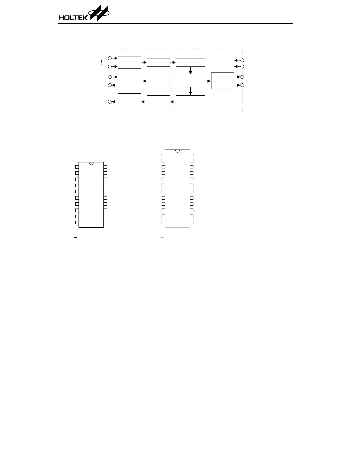
Block Diagram
HT817D0
KEY1
KEY12
OSC1
OSC2
AUD
Pin Assignment
KEY7
KEY8
KEY9
KEY10
KEY11
KEY12
NC
VDD
AUD
OSC2
H T 8 1 7 D 0
20 D IP/SO P
20
1
19
2
18
3
17
4
16
5
15
6
14
7
13
8
12
9
11
10
KEY6
KEY5
KEY4
KEY3
KEY2
KEY1
FLAG 2
VSS
FLAG 1
OSC1
D ebounce
Circuit
O scillator
Circuit
DAC &
O utput
C ontrol
One-shot
Tim e Base
G enerator
Voice RO M
96K ´ 6 -b it
KEY7
KEY8
KEY9
KEY10
KEY11
KEY12
NC
VDD
AUD
OSC2
OSC1
FLAG 1
Key Table
Table R O M
508
´
R O M A ddress
C ounter
1
2
3
4
5
6
7
8
9
10
11
12
24
23
22
21
20
19
18
17
16
15
14
13
H T 8 1 7 D 0
24 D IP/SO P
14-bit
KEY6
KEY5
KEY4
KEY3
KEY2
KEY1
NC
NC
NC
NC
FLAG 2
VSS
Status
Display
C ontroller
VDD
VSS
FLAG 1
FLAG 2
2 March 15, 2000
Page 3
HT817D0
Pad Assignment
KEY10
KEY11
KEY12
KEY9
1
19
2
3
KEY8
KEY7
KEY6
16
18
17
(0 ,0 )
KEY5
14
15
KEY4
13
KEY3
12
KEY2
11
KEY1
6
4
VDD
5
OSC2
AUD
Chip size: 2270 ´ 3630 (mm)
7
OSC1
10
8
9
VSS
FLAG 1
2
* The IC substrate should be connected to VSS in the PCB layout artwork.
Pad Coordinates
Pad No. X Y Pad No. X Y
1
2
3
4
5
6
-914.50
-914.50
-914.50
-987.90 -1638.25
-254.60 -1611.75
-18.90 -1611.75
7 411.90
8 674.70
9 806.10
10 937.90
1612.75 11 912.80 1115.95
1469.35 12 912.80 1254.55
1278.75 13 912.80 1449.95
14 912.80 1593.55
15 709.50 1564.05
16 179.20 1564.05
-1611.75
-1611.75
-1642.35
17 22.00 1564.05
18
19
-156.40
-734.20
-1611.75
3 March 15, 2000
FLAG 2
Unit: mm
1564.05
1564.05
Page 4
Pad Description
HT817D0
Pad No. Pad Name I/O
1~3 KEY10~KEY12 I Pull-high
4 VDD
5 AUD O
6 OSC2 O
7 OSC1 I
8 FLAG1 O
9 VSS
10 FLAG2 O
11~19 KEY1~KEY9 I Pull-high
Internal
Connection
¾¾
PMOS
Open Drain
¾
¾
NMOS
Open Drain
¾¾
NMOS
Open Drain
Absolute Maximum Ratings
Description
Trigger key, low active. Key features such as
debounce time, pull-high resistance and repeat
are all by mask option.
Positive power supply
Voice output for driving an external transistor
Oscillator output pin
Oscillator input pin
3HzB/6HzB flash output, busy output,
end-pulse or voice output indication (by mask
option). Open drain, active low output.
Negative power supply, ground
3Hz/6Hz flash output or busy output (by mask
option). Open drain, active low output.
Trigger key, active low. Key features such as
debounce time, pull-high resistance and repeat
are all by mask option.
Supply Voltage ................................-0.3V to 6V
Input Voltage ............... V
Note: These are stress ratings only. Stresses exceeding the range specified under ²Absolute Maxi-
mum Ratings² may cause substantial damage to the device. Functional operation of this device at other conditions beyond those listed in the specification is not implied and prolonged
exposure to extreme conditions may affect device reliability.
-0.3V to VDD+0.3V
SS
Storage Temperature ............... -50°Cto125°C
Operating Temperature .............-20°Cto70°C
4 March 15, 2000
Page 5
Electrical Characteristics
HT817D0
Symbol Parameter
Test Conditions
V
DD
V
I
I
I
I
V
V
f
DD
DD
STB
O
OL
IH
IL
OSC
Operating Voltage
¾¾
Operating Current 3V No load
Standby Current 3V
Max. AUD Output Current 3V
FLAG Sink Current 3V
²H² Input Voltage ¾¾
²L² Input Voltage ¾¾
Oscillating Frequency 3V
Functional Description
The HT817D0 is a mask ROM type voice synthe
sizer with 16.8-second voice capacity. A group of
pre-recorded voice sections is played upon receipt
of key trigger input signals. Two FLAG signals
are output while playing voices.
The 16.8-second voice capacity can be divided
into sections of arbitrary length. Notice that the
silence length and end-pulse width are not included in the memory.
By using Holtek¢s programming tools, the contents and arrangement of sections, as well as
key features and FLAG output are all programmable before device fabrication.
The IC provides 12 key inputs (KEY1~KEY12).
Of the 12 keys, KEY1 can be optioned as a direct, sequential or random trigger key. KEY12
can be selected as a stop or direct key. As for the
remaining 10 keys (KEY2~KEY11), they are
used as direct keys exclusively.
Conditions
Min. Typ. Max. Unit
3.6
¾¾
V
=0.6V
OH
V
=0.3V
OL
-1.5 -2 ¾
1.5 3.0
0.8V
=530kW
R
OSC
Play function block diagram
-
Key
trigger
76 96 116 kHz
Key
features
option
Playing control logic
¾
0
DD
Key
fu n c tio n
ta b le
ROM
¾
200 400
13
¾
¾
Voice
ROM
0.2V
5.0 V
¾
V
System oscillator
The HT817D0 has a built-in RC oscillator
which requires only one external resistor for
normal applications. The oscillator frequency
is typically 96kHz for an external resistor of
530kW. The required oscillator frequency may
vary with different sampling rates in the pro
cess of voice programming. As a result, the
value of the oscillator resistor may be differ
ent for different items.
DD
DD
D/A
Flag
output
V
mA
mA
mA
mA
V
V
DD
-
-
OSC1
R
HT817D0
OSC2
5 March 15, 2000
OSC
Page 6

HT817D0
The oscillator is turned on when triggered by a
key input. After playing, it is immediately turned
off and the chip goes into the standby state.
Voice ROM
The voice ROM is originally designed to continu
ously record the 16.8-second voice data at a 6kHz
sampling rate. Ahigher sampling rate can gener
ate voices of better playback quality, but will
shorten the total recording time. On the other
hand, a lower sampling rate results in longer re
cording time but sacrifice voice quality.
The playback time can be significantly extended
by making use of coding efficiency, silence play
ing, section repeating, section cascade, etc.
Section
Section is the basic element constituting the
contents of voice ROM. During programming,
the customer¢s voice sources can be divided into
as many sections as required. A section can be
composed of a voice or an interval of silence.
However, the silence length is not counted in
voice ROM. The total number of sections in
cluded should be less than 508 due to the space
limitation of the function table ROM. The total
length of the included sections is limited by
voice ROM.
A section, when triggered by a key input, can be
played once, repeatedly or cascaded with other
sections, depending on the key function table
instructions.
The following are examples of section division:
Exam ple 1: O ne section only
sec.1
ROM
Exam ple 2: 3 section division
sec.1 sec.2 sec.3
ROM
Exam ple 3: N section division
sec.2 sec.Nsec.1
ROM
In addition, a section can be set as retriggerable
or non-retriggerable depending on the code op
tion.
·
Retriggerable
-
-
When the currently playing section is set as
retriggerable, it will stop immediately upon
receipt of other key inputs.
·
Non-retriggerable
When the currently playing section is selected
-
as non-retriggerable, it will go on playing till
the whole section is completed, whether or not
there is a key input in the process of playing.
-
Of a key group, some sections can be set as
retriggerable and some as non-retriggerable.
When a retriggerable section of a key group is
playing, any key can be triggered to interrupt
its playing. On the other hand, if it is a
non-retriggerable section playing, any key in
terrupt is ignored.
Group
The HT817D0 plays groups on the basis of the
-
key input. A group can be made up of one or
more sections. When a key is triggered, the cor
responding group is played immediately. For
example, triggering KEY2 plays group 2, and so
on. The same section is allowed to appear in different groups. However, KEY1 can be made up
of multiple groups when it is optioned as a sequential or random key. Otherwise, each key is
comprised by one group only.
Key function table
The sections include in the voice ROM are
played according to the instructions of the key
function table. The function table contains
group information as well as playing order of
sections in the groups. Notice that the total
number of sections included in the groups
should be less than 508, the space limitation of
the function table ROM.
-
-
-
6 March 15, 2000
Page 7

HT817D0
·
KEY1 as a direct key
Each key is mapped to a group in the
function table. If a key is not used, the group
mapped to that key is a piece of silence.
The following is an example of the function ta
ble:
Group 1 sec.1 + sec.2 + sec.3 + sec.5
Group 2 sec.3
Group 3 sec.2 + sec.2 + sec.3 + sec.4
Group 4 sec.5 + sec.3
As illustrated in the above table, voice ROM is
composed of 5 sections and the function table
of 11 sections. If KEY1 is momentarily trig
gered, section 1, section 2, section 3 and sec
tion 5 are played in sequence and then
stopped. Triggering KEY2 plays section 3,
and so forth.
·
KEY1 as a sequential or random key
When KEY1 is optioned as a sequential or ran
dom key, it can include multiple groups
(sub-groups) in the function table. However,
the remaining 11 keys (KEY2~KEY12) are used
as direct keys exclusively and comprise only
one group in the function table.
An example is shown below:
Group 1-1 sec.4 + sec.2
Group 1-2 sec.1 + sec.3
-
:
:
:
:
Group 1-N sec.2 + sec.3
Group 2 sec.2 + sec.3
Group 3 sec.3 + sec.5
Group 4 sec.1 + sec.5 + sec.2
As indicated in the above table, KEY1 can be
made up of sub-groups. Each time KEY1 is
triggered, the corresponding sub-groups are
-
-
played in sequence.
¨
The playing sequence of sequential KEY1 is:
Group 1-1 ® Group 1-2 ® Group 1-3 ..... ®
Group 1-N (the last group) ®Group 1-1 .....
¨
The playing sequence of random KEY1 is:
Group 1-3 ® Group 1-5 ..... ® Group 1-N ®
-
Group 1-3 ® Group 1-5 .....
That KEY1 functions as a random key is a
special case of sequential key, which com
bines a particular arrangement of sub-group
playing sequence.
KEY1
KEY2~KEY12
AUD
KEY1
KEY2~KEY12
(Silence)
AUD
G roup 1-1 G roup 1-2 G roup 1-N G roup (2~12) G roup 1-1
Figure1 Reset of KEY1 playing sequence
N pulse
G roup 1-N
M pulse
G roup 1-M
Figure 2 KEY1 sub-group selection
7 March 15, 2000
Page 8

HT817D0
¨
Reset of KEY1 playing sequence
If a sub-group of KEY1is playing and one of
KEY2~KEY12 is triggered, the playing
sub-group will be terminated, and the newly
triggered key group come into play instead.
The first sub-group will start playing by
retriggering KEY1. Inother words, theKEY1
playing sequence is reset whenever a key
otherthanKEY1 is triggered (see Figure1).
¨
Sub-group selection
When KEY1 is triggered with pulses, a de
sired sub-group can be selected by controlling
its corresponding pulse number. However,
the features of KEY1 have to be set in the fol
lowing ways:
-
sequential or random
-
retriggerable
-
minimum key debounce time
(@700ms, f
OSC
=96kHz)
For instance, if sub-group 1-3 is the previous
playing group, sub-group 1-5 will start playing
after 2 pulses are input to KEY1, and so on.
To make easy selection of KEY1 sub-groups,
one of KEY2~KEY12 should be programmed
as silence. Then this silence key has to be
triggered to reset KEY1. By so doing, the
playing sub-group of KEY1 is directly specified by the pulse number applied to KEY1
(see Figure 2).
·
KEY12 as a stop key (by mask option)
When KEY12 functions as a stop key, any
voice output can be stopped by pressing
KEY12.
·
KEY1~KEY11 as a repeat key
KEY1~KEY11 all function as repeat key if
one of the eleven keys is set as a repeat key. In
other words, once the mode of one of
KEY1~KEY11 is determined, the remaining
10 keys are set accordingly.
As a repeat key, the sections included can be
played sequentially and repeatedly till other
key input is triggered. KEY12 has no other
choice but functions as a stop key when
KEY1~KEY11 are set as repeat keys.
-
-
Key features
·
Key priority
When two or more keys are triggered simulta
neously, the output voice is determined by the
key priority as shown below:
KEY1>KEY2>......KEY11>KEY12
·
Key debounce time
There are four kinds of key-in debounce time
that can be selected by mask option, namely,
700ms, 22ms, 45ms and 180ms. The key
debounce time varies with the value of the sys
tem frequency.
·
Pull-high resistance
Four kinds of key input pin pull-high resis
tance can be selected by mask option,
namely, 20kW, 50kW, 100kW and 200kW.
The resistance may vary with VDD, tem
peratures and the chip itself due to process
variations.
·
Trigger mode
All of the 12 keys can be optioned as one-shot
trigger mode, level hold mode or level-trigger
mode.
¨
One shot
When one of the 12 keys (KEY1~KEY12) is
pressed momentarily or held down, the
group corresponding to that key will play
once.
KEY N
AUD
¨
Level trigger
G roup N
G roup N
When one of the 12 keys is pressed and held
down, the corresponding group will keep
playing. Once the pressed key is released,
the group will not stop till the included sec
tions are all completed.
KEY N
AUD
G roup N
G roup N
G roup N
-
-
-
-
-
8 March 15, 2000
Page 9

HT817D0
¨
Level hold
When one of the 12 keys is pressed and held
down, the group corresponding to that held
key will play until the pressed key is re
leased, then the group will immediately
stop regardless of the rest.
KEY N
AUD
G roup N
G roup N
G roup N
FLAG
When voices are playing, both FLAG1 and
FLAG2 pins are activated to output one of the
following signals through code option.
FLAG1 can be optioned as one of the following
signal outputs:
None, 3HzB flash, Busy, 6HzB flash, Voice indica
tor, or End-pulse output
FLAG2, on the other hand, can be set as one of
the following signal outputs:
None, 3Hz flash, 6Hz flash, or Busy output
·
3Hz/3HzB flash
When voices are playing, the FLAG1 as well
as FLAG2 pin outputs a 3Hz signal to drive
an LED. The signal is active low, 25% duty.
Once the voice output is terminated, the
FLAG1 and FLAG2 pins become floating outputs. When the FLAG1 and the FLAG2 pins
are optioned as 3HzB and 3Hz outputs, they
will be alternately output at a 3Hz rate.
·
6Hz/6HzB flash
When voices are playing, the FLAG1 pin
outputs a 6Hz signal to drive an LED. The
-
signal is active low, 25% duty. Once the voice
output is terminated, the FLAG1 pin be
-
comes a floating output. When FLAG1 and
FLAG2 pins are optioned as 6HzB and 6Hz
outputs, they will be alternately output at a
6Hz rate.
AUD
FLAG
: F loating
·
Busy output
When a voice group is playing, the outputs of
-
both FLAG1 and FLAG2 are turned low, indi
-
cating that the chip is busy.
AUD
FLAG
: F lo a tin g
AUD
FLAG
: F loating
9 March 15, 2000
Page 10
HT817D0
In addition to the above-stated output sig
nals, FLAG1 can also generate one of the fol
lowing signals by code option:
¨
Voice indicator output
FLAG1 is active low when voices are play
ing. FLAG1 is also turned low when a voice
section is output. The brightness of FLAG1
varies with the volume. FLAG1 becomes
floating after the silence section is output or
the voice output is terminated.
AUD
FLAG
: F loating
¨
End-pulse output
When the voice output is completed, the
FLAG1 pin outputs an active low pulse. The
pulse width can be programmed depending
on the customer¢s requirements.
The FLAG1 as well as FLAG2 pins are both
floating outputs when the chip is in the
standby state.
Volume control
-
The function of volume control can be set by
mask option. A code is written in the function
table for the purpose of controlling the volume
of each section output after the volume control
function is chosen. There are two volume op
tions, namely, full range and half range.
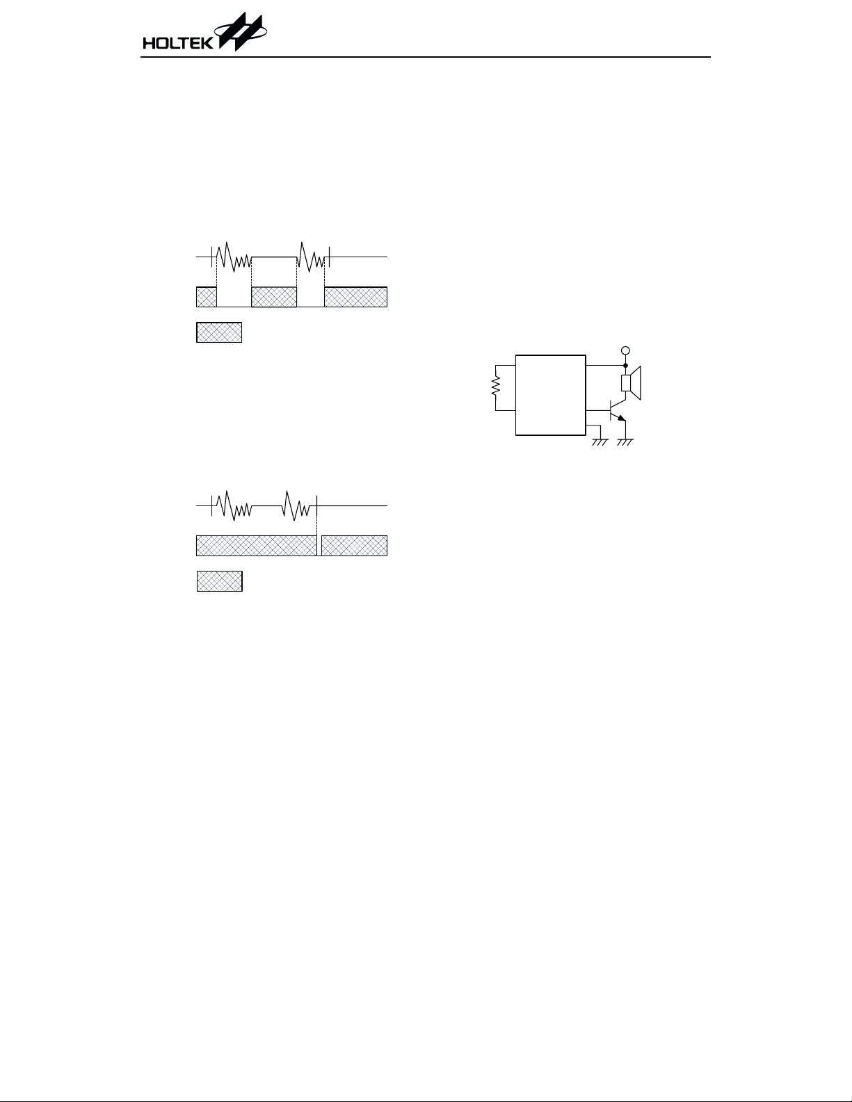
AUD
The AUD pin is a PMOS open drain structure.
It outputs voice signals to drive a speaker
through an external NPN transistor when the
chip is active. The AUD pin becomes a floating
output when the chip is in the standby state.
The 8050 type transistor with h
FE
ommended for an output driver.
OSC1
R
OSC
OSC2
VDD
AUD
VSS
8050
H T 817D 0
@150 is rec
V
DD
SPK
-
-
AUD
FLAG
: F loating
10 March 15, 2000
Page 11

Application Circuits
General application
HT817D0
SPK
8
KEY10
KEY11
KEY12
KEY9
1
2
19
3
KEY8
KEY7
KEY6
16
18
17
KEY5
KEY4
14
KEY3
13
15
KEY2
12
KEY1
11
H T817D 0
V
DD
6
4
W
VDD
8050
R
R
5
OSC2
AUD
7
Rosc
10
8
9
FLAG 1
OSC1
FLAG 2
VSS
* The IC substrate should be connected to VS S in the PC B layout artw ork.
V
DD
Rosc
VDD
FLAG 1
FLAG 2
AUD
NC
NC
NC
NC
NC
VSS
OSC2
8
12
14
9
7
15
16
17
18
13
10
R=100W~330
R
R
SPK
8
W
8050
W
19
20
21
22
23
24
1
2
3
4
5
6
11
KEY1
KEY2
KEY3
KEY4
KEY5
KEY6
KEY7
KEY8
KEY9
KEY10
KEY11
KEY12
OSC1
H T817D 0
11 March 15, 2000
Page 12

Parallel application
100W~
100W~
330
330
W
W
FLAG 1
FLAG 2 FLAG 1
VDD OSC2 O SC1
H T 817D 0
VSS KEY1 KEY12
Cascade or external driving
HT817D0
V
DD
100W~
100W~
330
R
OSC
330
AUD
W
W
FLAG 2
VDD OSC2 O SC1
R
OSC
H T 817D 0
VSS KEY1 KEY12
AUD
8050
V
DD
R
OSC
OSC2 OSC1
VSS KEY1
Power-on play (one shot)
0.1mF
KEY
FLAG 1
KEY12
R
OSC
1.2M
AUD
100W~
330
H T 817D 0
W
W
FLAG 1
100W~
330
trigger
out
FLAG 1 O SC2 OSC1
KEY
H T 817D 0H T 817D 0
VSS
W
FLAG 2 V DDOSC2 OSC1
AUD
VSS
V
DD
8050
R
OSC
AUD
SW
8050
12 March 15, 2000
Page 13

Power-on play (continuous)
With volume adjustment
KEY
HT817D0
V
DD
SW
100W~
100W~
330
W
330
FLAG 1
100W~
330
W
W
FLAG 2
VDDOSC2 OSC1
AUD
VSS
8050
V
DD
SW
R
OSC
H T 817D 0
100W~
330
OSC
W
R
KEY1
FLAG 1
H T 817D 0
KEY12
FLAG 2 VD DOSC2 OSC1
AUD
1k
8050
W
10mF
VSS
13 March 15, 2000
Page 14

HT817D0
Push-pull output
To prevent the speaker and driver transistor from damage due to excess power dissipation which re
sults from a high voltage power supply (4.5V~5.5V), the following push-pull output stage is recom
mended.
V
DD
SW
100W~
100W~
330
W
FLAG 1
W
FLAG 2
KEY12
VDDOSC2 OSC1
AUD
VSS
1N 4148
8050
8550
430
47mF
W
KEY1
Coupling to power amplifier
R
OSC
330
H T 817D 0
-
-
KEY1
R
OSC
100W~
330
W
FLAG 1
H T 817D 0
V
DD
100W~
330
W
FLAG 2
VDDOSC2 OSC1
VSS
0.1mF
560
To
W
pow er
10k
W
am p
AUD
KEY12
14 March 15, 2000
Page 15

HT817D0
Holtek Semiconductor Inc. (Headquarters)
No.3 Creation Rd. II, Science-based Industrial Park, Hsinchu, Taiwan, R.O.C.
Tel: 886-3-563-1999
Fax: 886-3-563-1189
Holtek Semiconductor Inc. (Taipei Office)
5F, No.576, Sec.7 Chung Hsiao E. Rd., Taipei, Taiwan, R.O.C.
Tel: 886-2-2782-9635
Fax: 886-2-2782-9636
Fax: 886-2-2782-7128 (International sales hotline)
Holtek Semiconductor (Hong Kong) Ltd.
RM.711, Tower 2, Cheung Sha Wan Plaza, 833 Cheung Sha Wan Rd., Kowloon, Hong Kong
Tel: 852-2-745-8288
Fax: 852-2-742-8657
Copyright Ó 2000 by HOLTEK SEMICONDUCTOR INC.
The information appearing in this Data Sheet is believed to be accurate at the time of publication. However, Holtek
assumes no responsibility arising from the use of the specifications described. The applications mentioned herein are
used solely for the purpose of illustration and Holtek makes no warranty or representation that such applications
will be suitable without further modification, nor recommends the use of its products for application that may pres
ent a risk to human life due to malfunction or otherwise. Holtek reserves the right to alter its products without prior
notification. For the most up-to-date information, please visit our web site at http://www.holtek.com.tw.
15 March 15, 2000
-
 Loading...