

Page 1
PHOTOVOLTAIC SOLID-STATE
RELAY OPTOCOUPLERS
HSR312 HSR312L HSR412 HSR412L
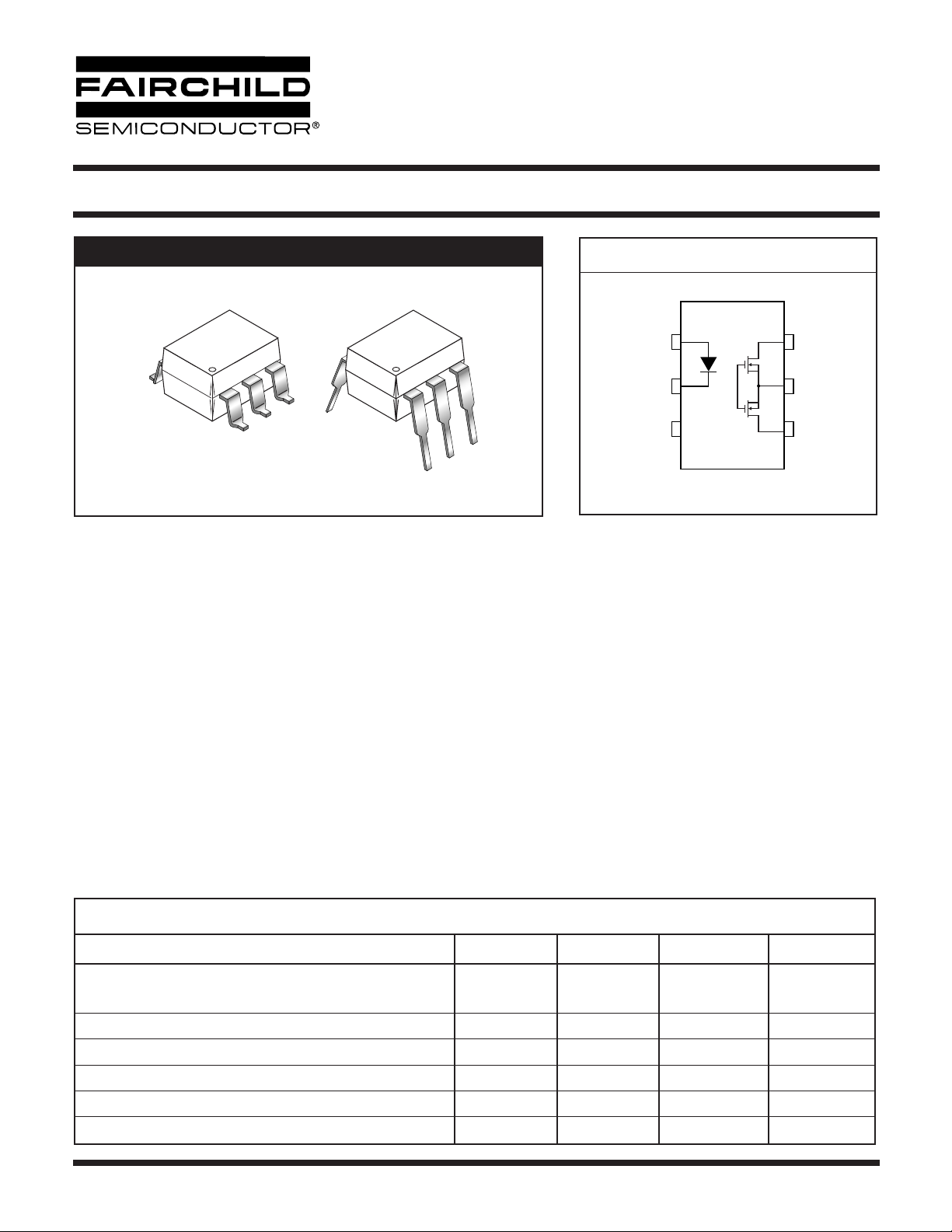
PACKAGE
6
6
CATHODE
SCHEMATIC
ANODE
1
2
3
N/C
6
5
4
DRAIN
DRAIN
1
1
DESCRIPTION
The HSR312 and HSR412 devices consist of a AlGaAs infrared emitting diode optically coupled to a power MOSFET detector
which is driven by a photovoltaic generator. The devices are housed in a 6-pin dual-in-line package. The HSR312L and HSR412L
employ an active current limit circuitry enabling the device to withstand current surge transients.
FEATURES
• 4,000 VRMS Isolation
• Wide operating voltage range
– 250 V (HSR312, HSR312L)
– 400 V (HSR412, HSR412L)
• Solid-State Reliability
• Bounce-Free Operation
• 4000 V ESD Rating (HBM)
• UL, CSA and BABT approval pending
APPLICATIONS
• On/Off Hook Switch • Replacement for Mechanical Relays
• Dial Out Relay • Ring Injection Relay
• General Switching • Ground Start
(T
ABSOLUTE MAXIMUM RATINGS
Parameters Symbol Device Value Units
TOTAL DEVICE
Storage Temperature
Operating Temperature
Lead Solder Temperature
Isolation Surge Voltage
Maximum Input/Output Capacitance
Maximum Input/Output Resistance
© 2003 Fairchild Semiconductor Corporation
= 25°C unless otherwise noted)
A
T
STG
T
OPR
T
SOL
V
ISO
C
IO
R
IO
Page 1 of 8
All -40 to +100 °C
All -40 to +85 °C
All 260 for 10 sec °C
All 4000 Vac(RMS)
All 1.0 pF
All
10
12
Ω
1/28/03
Page 2
Ω
PHOTOVOLTAIC SOLID-STATE
RELAY OPTOCOUPLERS
HSR312 HSR312L HSR412 HSR412L
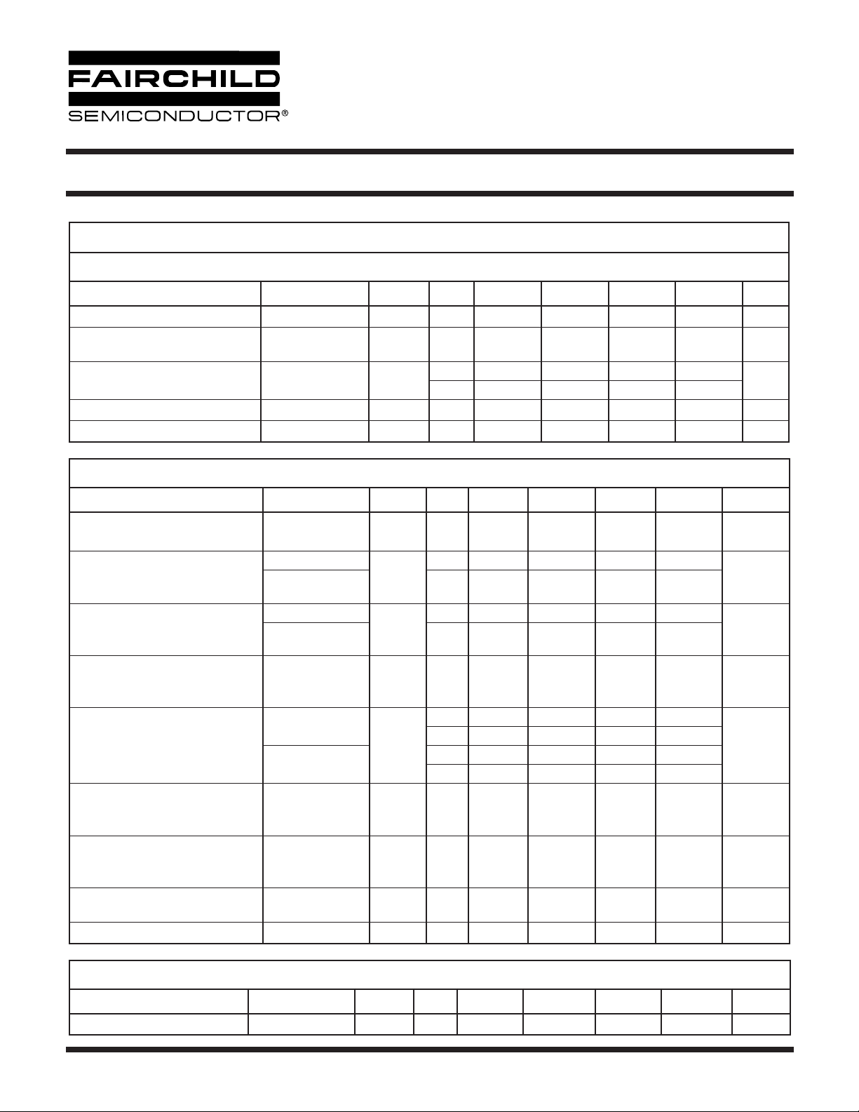
ELECTRICAL CHARACTERISTICS
(T
= -40°C to +85°C Unless otherwise specified)
A
INPUT CHARACTERISTICS
Parameters/Test Conditions Connection Symbol Limit HSR312 HSR312L HSR412 HSR412L Units
Control Current Series or Parallel
Control Current for Off-State
Resistance
Series or Parallel
Control Current Range Series or Parallel
Reverse Voltage Series or Parallel
Forward Voltage (I
=10 mA)
F
Series or Parallel
I
F(ON)
I
F(OFF)
I
F
V
V
Max 2.0 2.0 3.0 3.0 mA
Min 0.4 0.4 0.4 0.4 mA
Min 2.0 2.0 3.0 3.0
Max 25 25 25 25
R
F
Min7777V
Max 1.6 1.6 1.6 1.6 V
OUTPUT CHARACTERISTICS
Parameters / Test Conditions Connection Symbol Limit HSR312 HSR312L HSR412 HSR412L Units
V
Operating Voltage Range Series or Parallel
Load Current
T
= +40°C, 5mA control
A
(see fig. 1 & 2)
On-State Resistance
T
= 25°C, 50mA pulsed load,
A
5mA control
Series
Parallel Max 320 300 210 200
Series
Parallel Max 3 4.25 7 9
Off-State Leakage Current
T
= 25°C, ±250V for HSR312/L,
A
Series or Parallel — Max 1.0 1.0 1.0 1.0 µA
±400V for HSR412/L
Current Limit
T
= +25°C, 5mA control
A
Series
Parallel
Turn-On Time
T
= +25°C for 50mA,
A
Series or Parallel
100VDC load, 5mA control
Turn-Off Time
T
= +25°C for 50mA,
A
Series or Parallel
100VDC load, 5mA control
Thermal Offset Voltage
5mA control
Output Capacitance 5V
DC
Series or Parallel — Max N/A N/A 0.5 0.5 mV
Series or Parallel
V
R
I
T
T
OPR
I
L
ON
LMT
ON
OFF
C
O
Max 250 250 400 400
Max 190 170 140 120
Max 10 15 27 35
Min N/A 190 N/A 130
Max N/A 300 N/A 220
Min N/A 330 N/A 260
Max N/A 560 N/A 440
Max 3.0 3.0 2.0 2.0 mS
Max 0.5 0.5 0.5 0.5 mS
Max 50 50 12 12 pF
DC
V
AC(PEAK)
mA
mA
mA
or
ISOLATION CHARACTERISTICS
Characteristics Test Conditions Symbol Limit HSR312 HSR312L HSR412 HSR412L Units
Input-Output Isolation Voltage
© 2003 Fairchild Semiconductor Corporation
V
ISO
Page 2 of 8
Max 4000 4000 4000 4000 V
1/28/03
Page 3
PHOTOVOLTAIC SOLID-STATE
RELAY OPTOCOUPLERS
HSR312 HSR312L HSR412 HSR412L
20.0
17.5
15.0
(mA)
F
12.5
10.0
85°C
7.5
5.0
25°C
-40°C
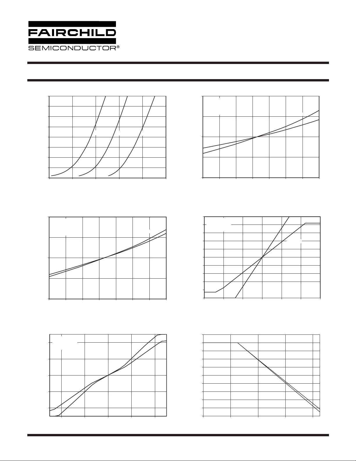
FORWARD CURRENT, I
2.5
0.0
1.0 1.1 1.2 1.3 1.4 1.5
FORWARD VOLTAGE, VF (V)
Figure 3. Normalized on Resistance vs. Ambient Temperature
2
Figure 1. Forward Current vs. Forward Voltage
)
Ω
(
NORMALIZED ON RESISTANCE, R
Series Connection
5mA Control
I
ON
= 10mA
D
Normalized at 25
1
0
-40 -20 0 20 40 60 80 100
°C
AMBIENT TEMPERATURE, T
A
HSR412L
(°C)
HSR412
Figure 2. Normalized on Resistance vs. Ambient Temperature
2
)
Series Connection
Ω
5mA Control
(
= 10mA
I
D
ON
Normalized at 25
1
°C
HSR312L
HSR312
NORMALIZED ON RESISTANCE, R
0
-40 -20 0 20 40 60 80 100
AMBIENT TEMPERATURE, TA (°C)
Figure 4. Load Current vs. Voltage Drop
250
Series Connection
200
5mA Control
@25°C, pulsed
150
100
(mA)
DD
50
0
-50
-100
LOAD CURRENT, I
-150
-200
-250
-3 -2 -1 0 1 2 3
VOLTAGE DROP, VDD (V)
HSR312
HSR312L
Figure 5. Load Current vs. Voltage Drop
Series Connection
200
5mA Control
@25°C, pulsed
100
(mA)
DD
0
-100
HSR412L
HSR412
LOAD CURRENT, I
-200
-4 -2 0 2 4
VOLTAGE DROP, VDD (V)
© 2003 Fairchild Semiconductor Corporation
Page 3 of 8
Figure 6. Maximum Load Current Vs Ambient Temperature
202
Vdd = 4V
200
198
(mA)
dd
196
194
192
190
188
186
Maximum Load Current, I
184
182
020406080
Ambient Temperature, TA (°C)
Series Connection
HSR312
I
= 5mA
F
= 2mA
I
F
1/28/03
Page 4
PHOTOVOLTAIC SOLID-STATE
RELAY OPTOCOUPLERS
HSR312 HSR312L HSR412 HSR412L
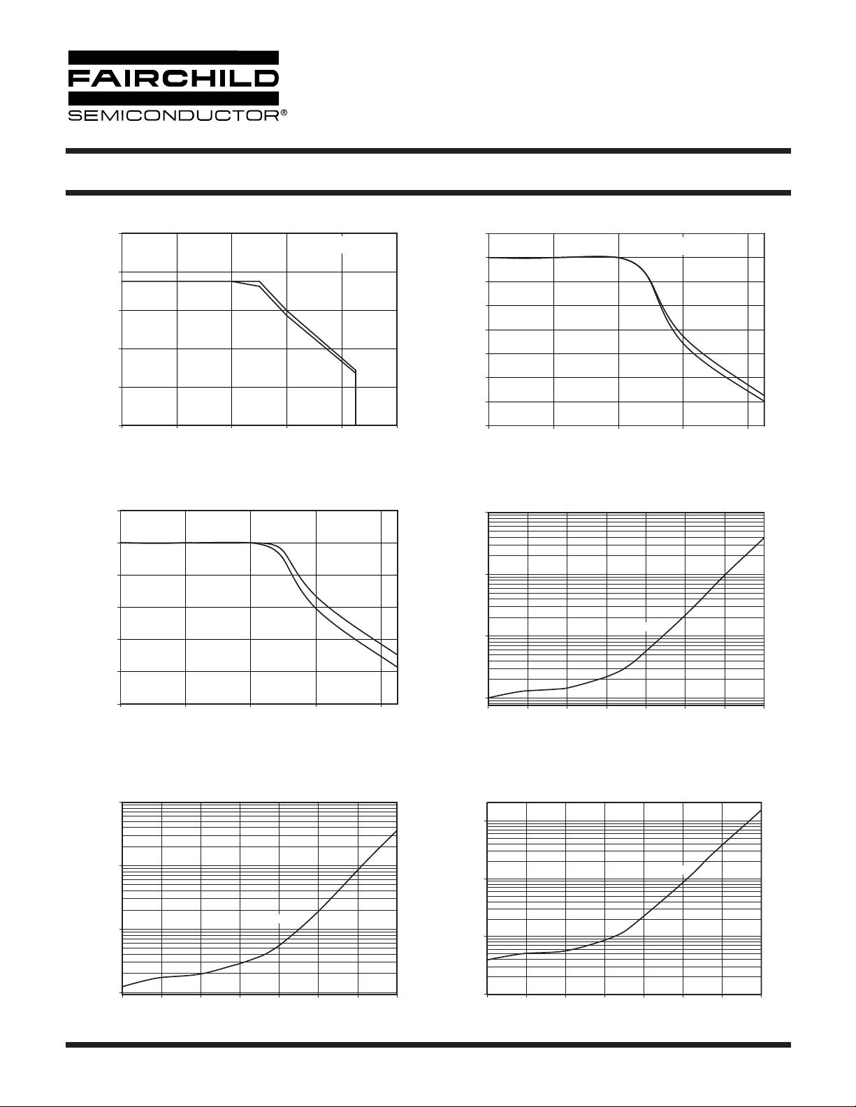
Figure 7. Maximum Load Current Vs Ambient Temperature Figure 8. Maximum Load Current Vs Ambient Temperature
200
Vdd = 4V
180
(mA)
dd
160
140
120
Maximum Load Current, I
100
0 20406080100
Series Connection
HSR312L
= 5mA
I
F
I
= 2mA
F
Ambient Temperature, TA (°C)
145
Vdd = 4V
140
(mA)
135
dd
130
125
120
115
Maximum Load Current, I
110
105
020406080
Series Connection
HSR412
= 5mA
I
F
I
= 3mA
F
Ambient Temperature, TA (°C)
Figure 9. Maximum Load Current Vs Ambient Temperature
125
Vdd = 4V
120
(mA)
dd
115
110
105
Maximum Load Current, I
100
95
020406080
Series Connection
HSR412L
I
= 5mA
F
= 3mA
I
F
Ambient Temperature, TA (°C)
Figure 11. Off State Current vs. Ambient Temperature
1000
(nA)
OFF
100
10
HSR412/L
Figure 10. Off State Current vs. Ambient Temperature
1000
(nA)
OFF
100
10
HSR312/L
OFF STATE CURRENT, I
1
-40 -20 0 20 40 60 80 100
AMBIENT TEMPERATURE, TA (°C)
Figure 12. Normalized Off State Leakage vs.
Ambient Temperature
100
C
°
@25
D-OFF
/I
D-OFF
I
10
1
HSR312/L
OFF STATE CURRENT, I
1
-40 -20 0 20 40 60 80 100
AMBIENT TEMPERATURE, TA (°C)
© 2003 Fairchild Semiconductor Corporation
Page 4 of 8
0.1
-40 -20 0 20 40 60 80 100
AMBIENT TEMPERATURE, T
A
(°C)
1/28/03
Page 5
PHOTOVOLTAIC SOLID-STATE
RELAY OPTOCOUPLERS
HSR312 HSR312L HSR412 HSR412L
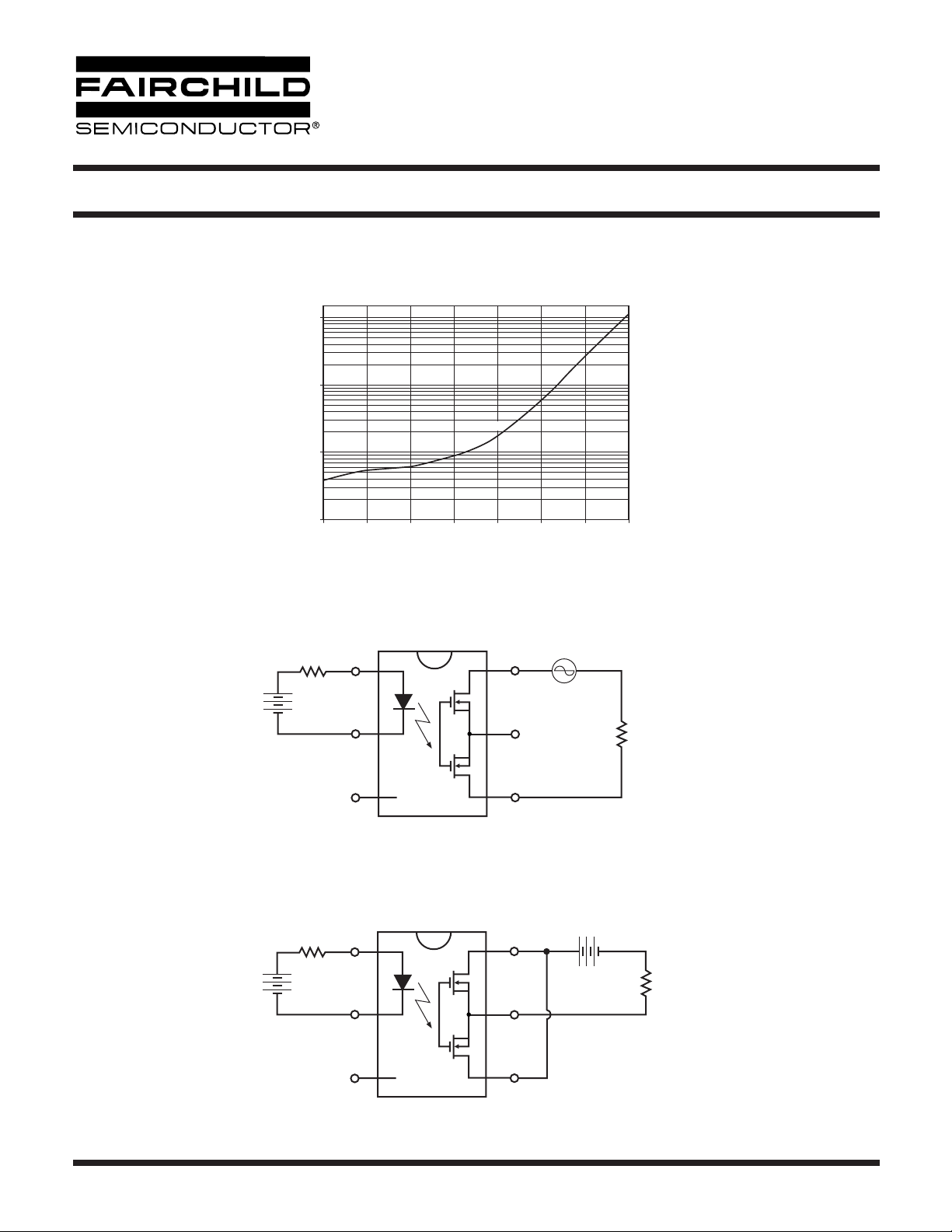
Figure 13. Normalized Off State Leakage vs.
100
C
°
10
@25
D-OFF
/I
D-OFF
1
I
0.1
-40 -20 0 20 40 60 80 100
Ambient Temperature
HSR412/L
AMBIENT TEMPERATURE, TA (°C)
Series Connection
1
+
2
6
5
AC or DC
LOAD
+
© 2003 Fairchild Semiconductor Corporation
3
Parallel Connection
1
2
3
Page 5 of 8
4
6
5
4
+
LOAD
1/28/03
Page 6
)
)
)
)
)
)
PHOTOVOLTAIC SOLID-STATE
RELAY OPTOCOUPLERS
HSR312 HSR312L HSR412 HSR412L
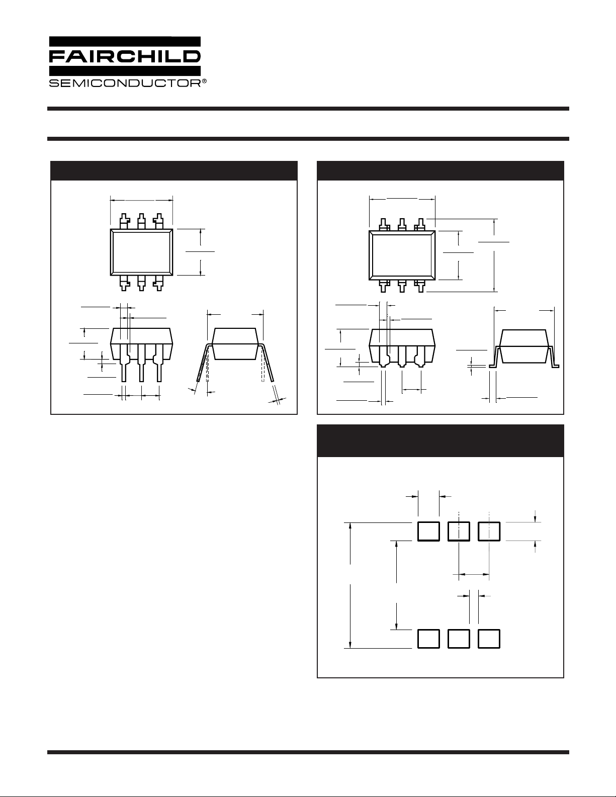
Package Dimensions (Through Hole) Package Dimensions (Surface Mount)
0.070 (1.77)
0.040 (1.02)
0.200 (5.08)
0.115 (2.93)
0.100 (2.54)
0.015 (0.38)
0.020 (0.50)
0.016 (0.41)
0.350 (8.89)
0.320 (8.13)
0.014 (0.36)
0.010 (0.25)
0.100 (2.54)
0.260 (6.60)
0.240 (6.10)
0.320 (8.13)
15°
0.012 (0.30)
0.350 (8.89)
0.320 (8.13)
0.260 (6.60)
0.240 (6.10)
0.070 (1.77)
0.040 (1.02)
0.200 (5.08)
0.115 (2.93)
0.025 (0.63)
0.020 (0.51)
0.020 (0.50)
0.016 (0.41)
0.014 (0.36)
0.010 (0.25)
0.100 [2.54]
0.012 (0.30)
0.008 (0.20)
Recommended Pad Layout for
Surface Mount Leadform
0.390 (9.90)
0.332 (8.43)
0.320 (8.13)
0.035 (0.88)
0.006 (0.16)
NOTE
All dimensions are in inches (millimeters)
© 2003 Fairchild Semiconductor Corporation
Page 6 of 8
0.425 (10.79
0.100 (2.54
0.305 (7.75
0.070 (1.78
0.060 (1.52
0.030 (0.76
1/28/03
Page 7
PHOTOVOLTAIC SOLID-STATE
RELAY OPTOCOUPLERS
HSR312 HSR312L HSR412 HSR412L
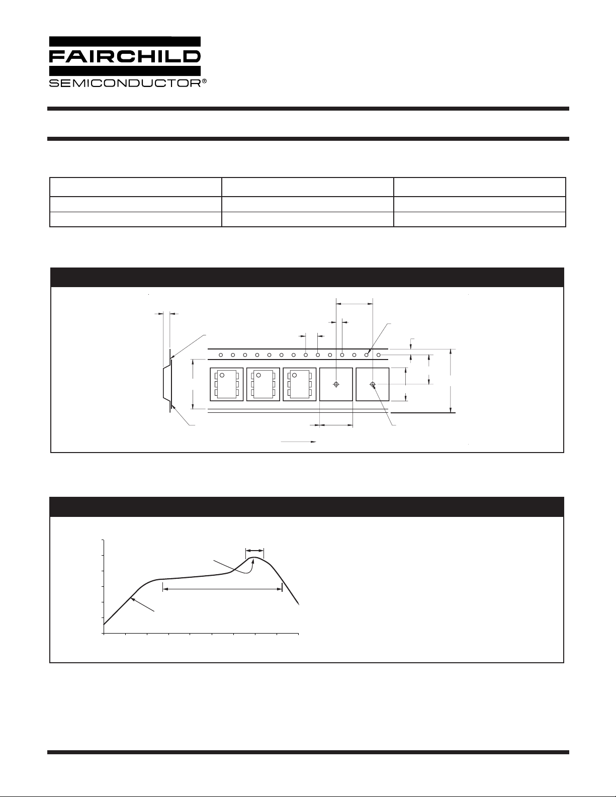
ORDERING INFORMATION
Option Order Entry Identifier Description
S S Surface Mount Lead Bend
SR2 SR2 Surface Mount; Tape and reel
Carrier Tape Specifications (“D” Tapin Orientation)
4.5 ± 0.20
21.0 ± 0.1
0.1 MAX
NOTE
All dimensions are in inches (millimeters)
Reflow Profile
300
250
200
150
100
Temperature (°C)
50
0
0.5 1 1.5 2 2.5 3 3.5 4 4.5
0
245°C peak
Time above 183°C, 120–180 sec
Ramp up = 2–10°C/sec
Time (Minute)
0.30 MAX
User Direction of Feed
230°C, 10–30 s
4.0 ± 0.1
10.1 ± 0.20
12.0 ± 0.1
2.0 ± 0.05
1.5 MIN
Ø
1.75 ± 0.10
11.5 ± 1.0
9.1 ± 0.20
Ø
• Peak reflow temperature: 245°C (package surface temperature)
• Time of temperature higher than 183°C for 120–180 seconds
• One time soldering reflow is recommended
24.0 ± 0.3
1.5 ± 0.1/-0
© 2003 Fairchild Semiconductor Corporation
Page 7 of 8
1/28/03
Page 8

PHOTOVOLTAIC SOLID-STATE
RELAY OPTOCOUPLERS
HSR312 HSR312L HSR412 HSR412L
DISCLAIMER
FAIRCHILD SEMICONDUCTOR RESERVES THE RIGHT TO MAKE CHANGES WITHOUT FURTHER NOTICE TO
ANY PRODUCTS HEREIN TO IMPROVE RELIABILITY, FUNCTION OR DESIGN. FAIRCHILD DOES NOT ASSUME
ANY LIABILITY ARISING OUT OF THE APPLICATION OR USE OF ANY PRODUCT OR CIRCUIT DESCRIBED HEREIN;
NEITHER DOES IT CONVEY ANY LICENSE UNDER ITS PATENT RIGHTS, NOR THE RIGHTS OF OTHERS.
LIFE SUPPORT POLICY
FAIRCHILD’S PRODUCTS ARE NOT AUTHORIZED FOR USE AS CRITICAL COMPONENTS IN LIFE SUPPORT DEVICES
OR SYSTEMS WITHOUT THE EXPRESS WRITTEN APPROVAL OF THE PRESIDENT OF FAIRCHILD SEMICONDUCTOR
CORPORATION. As used herein:
1. Life support devices or systems are devices or systems
which, (a) are intended for surgical implant into the body, or
(b) support or sustain life, and (c) whose failure to perform
when properly used in accordance with instructions for use
provided in the labeling, can be reasonably expected to
result in a significant injury of the user.
2. A critical component in any component of a life support
device or system whose failure to perform can be
reasonably expected to cause the failure of the life support
device or system, or to affect its safety or effectiveness.
© 2003 Fairchild Semiconductor Corporation
Page 8 of 8
1/28/03
 Loading...