

Page 1
HSP9520, HSP9521
Data Sheet May 1999
Multilevel Pipeline Registers
These devices are multilevel pipeline registers implemented
using a low power CMOS process. They are pin for pin
compatible replacements for industry standard multilevel
pipeline registers such as the L29C520 and L29C521. The
HSP9520 and HSP5921 are direct replacements for the
AM29520 and AM29521 and WS59520 and WS59521.
They consist of four 8-bit registers which are dual ported.
They can be configured as a single four level pipeline or a
dual two level pipeline. A single 8-bit input is provided, and
the pipelining configuration is determined by the instruction
code input to the I0 and I1 inputs (see instruction control).
The contents of any of the four registers is selectable at the
multiplexed outputs through the use of the S0 and S1
multiplexercontrol inputs (see register select. The output is 8
bits wide and is three-stated through the use ofthe
OE input.
The HSP9520 and HSP9521 differ only in the way data is
loaded into and between the registers in dual two-level
operation. In the HSP9520 when data is loaded into the first
levelthe existingdata inthe firstlevel is movedto thesecond
level. In the HSP9521 loading the first level simply causes
the current data to be overwritten. Transfer of data to the
second level is achievedusing the singlefour level mode(I1,
I0 = ‘0’). This instruction also causes the first level to be
loaded. TheHOLD instruction (I1, I0 = ‘1’) providesa means
of holding the contents of all registers.
Ordering Information
TEMP.
PART NUMBER
HSP9520CP 0 to 70 24 Ld PDIP E24.3
HSP9520CS 0 to 70 24 Ld SOIC M24.3
HSP9521CP 0 to 70 24 Ld PDIP E24.3
HSP9521CS 0 to 70 24 Ld SOIC M24.3
RANGE (oC) PACKAGE
PKG.
NO.
File Number
Features
• Four 8-Bit Registers
• Hold, Transfer and Load Instructions
• Single 4-Stage or Dual-2 Stage Pipelining
• All Register Contents Available at Output
• Fully TTL Compatible
• Three-State Outputs
• High Speed, Low Power CMOS
Applications
• Array Processor
• Digital Signal Processor
• A/D Buffer
• Telecommunication
• Byte Wide Shift Register
• Mainframe Computers
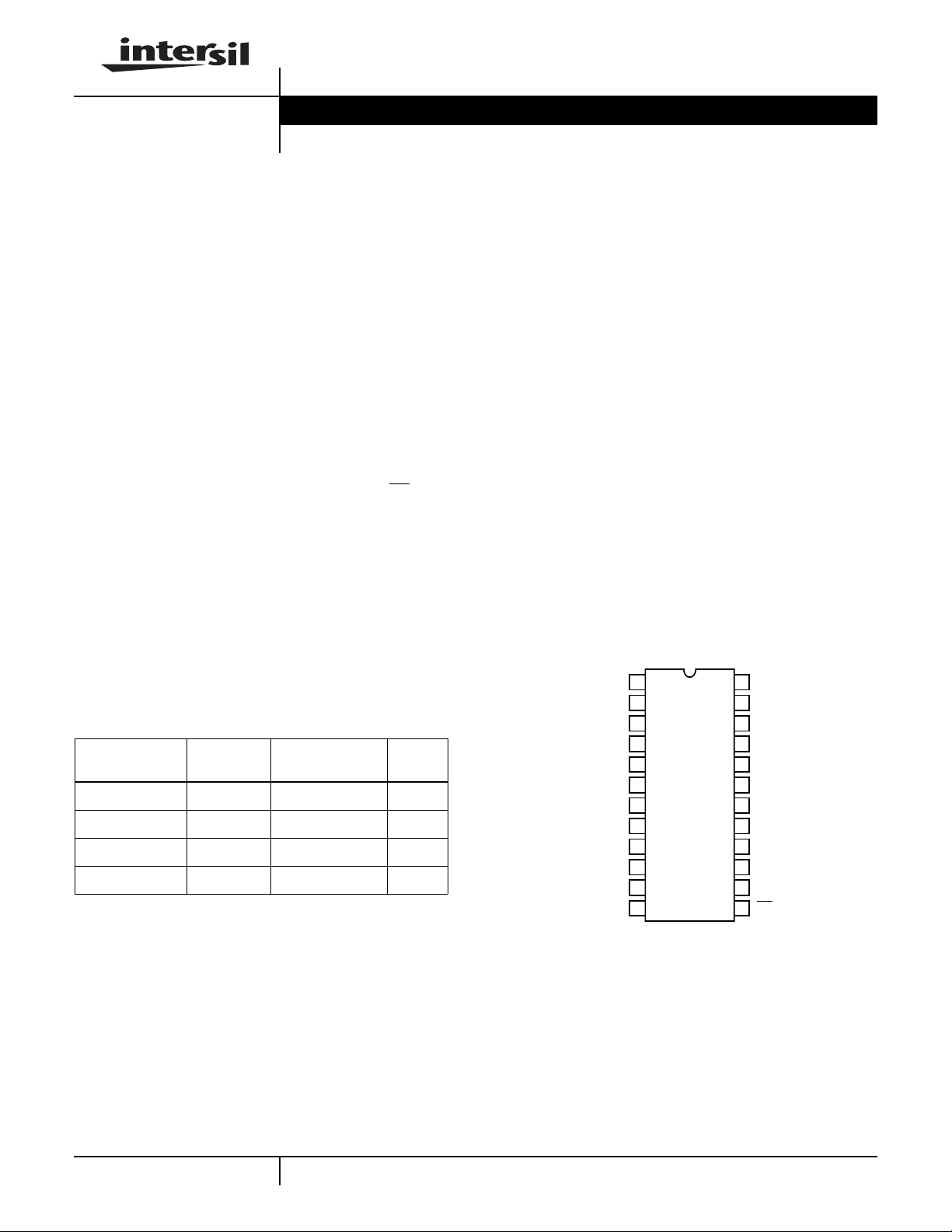
Pinout
HSP9520, HSP9521 (SOIC, PDIP)
TOP VIEW
V
24
23
S0
S1
22
Y0
21
Y1
20
Y2
19
Y3
18
Y4
17
16
Y5
Y6
15
Y7
14
OE
13
D0
D1
D2
D3
D4
D5
D6
D7
CLK
GND
I0
1
I1
2
3
4
5
6
7
8
9
10
11
12
2811.5
CC
1
CAUTION: These devices are sensitive to electrostatic discharge; follow proper IC Handling Procedures.
http://www.intersil.com or 407-727-9207 | Copyright © Intersil Corporation 1999
Page 2
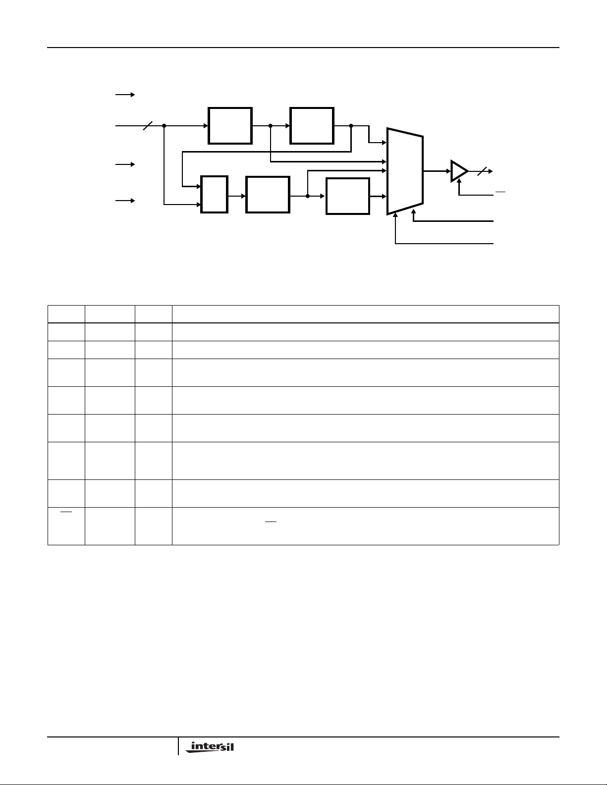
Block Diagram
I0
HSP9520, HSP9521
D0 - D7
CLK
8
I1
REG. A1 REG. A2
MUX
REG. B1
REG. B2
MUX
8
Y0 - Y7
OE
S0
S1
Pin Descriptions
NAME DIP PIN TYPE DESCRIPTION
V
CC
GND 12 The device ground.
CLK 11 I Input Clock. Data is latched on the low to high transition of this clock signal. Input setup and hold times with
D0-7 3-10 I Data Input Port. These inputs are used to supply the 8 bits of data which will be latched into the selected
24 The +5V Power Supply Pin. A 0.1µF capacitor between the VCC and GND pin is recommended.
respect to the clock must be met for proper operation.
register on the next rising clock edge.
Y0-7 21-14 O DataOutput Port. This 8-bit portprovides the output data fromthe four internalregisters. Theyare provided in
a multiplexed fashion, and are controlled via the multiplexer control inputs (S0 and S1).
I0, I1 1, 2 I InstructionControl Inputs. Theseinputs are usedto provide theinstruction code whichdetermines the internal
registerpipeline configuration. Refer totheInstructionControl Table forthespecificcodes and their associated
configurations.
S0, S1 23, 22 I Multiplexer Control Inputs. These inputs select whichof thefour internal registers contents will be availableat
the output port. Refer to the Register Select Table for the codes to select each register.
OE 13 I Output Enable. This input controls the state of the output port (Y0 - Y7). A LOW on this control line enables
the portfor output. When OE isHIGH, the output drivers arein the high impedance state.Internal latching or
transfer of data is not affected by this pin.
2
Page 3

HSP9520, HSP9521
Absolute Maximum Ratings Thermal Information
Supply Voltage . . . . . . . . . . . . . . . . . . . . . . . . . . . . . . . . . . . . +8.0V
Input or Output Voltage Applied. . . . . . . . . . GND -0.5 to VCC +0.5V
Operating Conditions
Voltage Range. . . . . . . . . . . . . . . . . . . . . . . . . . . . . -4.75V to 5.25V
Temperature Range. . . . . . . . . . . . . . . . . . . . . . . . . . . 0oC to 70oC
CAUTION: Stresses above those listed in “Absolute Maximum Ratings” may cause permanent damage to the device. This is a stress only rating and operationofthe
device at these or any other conditions above those indicated in the operational sections of this specification is not implied.
NOTE:
1. θJA is measured with the component mounted on an evaluation PC board in free air.
Thermal Resistance (Typical, Note 1) θJA (oC/W)
PDIP Package . . . . . . . . . . . . . . . . . . . 67
SOIC Package . . . . . . . . . . . . . . . . . . . 77.0
Maximum Junction Temperature . . . . . . . . . . . . . . . . . . . . . . .150oC
Maximum Storage Temperature Range. . . . . . . . . . -65oC to 150oC
Maximum Lead Temperature (Soldering 10s) . . . . . . . . . . . . .300oC
DC Electrical Specifications V
= 5.0V ±5%, TA = 0oC to 70oC
CC
PARAMETER SYMBOL TEST CONDITIONS MIN MAX UNITS
Logical One Input Voltage V
Logical Zero Input Voltage V
Output HIGH Voltage V
Output LOW Voltage V
Input Leakage Current I
Output Leakage Current I
Standby Power Supply Current I
Operating Power Supply Current I
CCSB
CCOP
VCC = 5.25V 2.0 - V
IH
VCC = 4.75V - 0.8 V
IL
IOH = -6.5mA, VCC - 4.75V 2.4 - V
OH
IOH = +20.0mA, VCC = 4.75V - 0.5 V
OL
VIN = VCC or GND, VCC = 5.25V -10 -10 µA
I
V
O
= VCC or GND, VCC = 5.25V -10 -10 µA
OUT
VIN = VCC or GND, VCC = 5.25V Outputs Open - 500 µA
f = 5.0MHz, VIN = VCC or GND, VCC = 5.25V, Outputs
-12mA
Open (Note 2)
Input Capacitance CIN FREQ = 1MHZ, VCC = Open, All Measurements are
Output Capacitance CO - 12 pF
AC Electrical Specifications V
= 5.0V ±5%, TA = 0oC to 70oC (Note 3)
CC
Referenced to Device Ground
-12pF
PARAMETER SYMBOL TEST CONDITIONS MIN MAX UNITS
Clock to Data Out t
Mux Select to Data Out t
Input Setup Time (DO-7/10-7) t
Input Hold Time (DO-7/10-7) t
Output Enable Time t
Output Disable Time t
Clock Pulse Width t
PD
SELD
S
H
ENA
DIS
PW
(Note 4) - 13 ns
-21ns
-20ns
10 - ns
3-ns
-20ns
10 - ns
NOTES:
2. Power supply current is proportional to frequency. Typical rating for I
is 2.4mA/MHz.
CCOP
3. AC Testing is performed as follows: Inputlevels: 0V and 3.0V, timing reference levels= 1.5V, input rise and fall timesdriven at1ns/V, output
load CL = 40pF.
4. Controlled by design or process parameters andnot directlytested. Characterized upon initial design and after major designand/or process
changes.
3
Page 4

Timing Waveform
CLOCK
(CLK)
INST
(I0 - I1)
DAT A
(S0 - D7)
MUX SEL
(S0 - S1)
OUT
(Y0 - Y7)
HSP9520, HSP9521
t
PW
t
t
S
t
S
t
SELD
H
t
H
t
PD
1.5V
t
PW
THREE STATE
CONTROL
THREE STATE
OUTPUT
(Y0 - Y7)
OE
TABLE 1. INSTRUCTION CONTROL
I1 I0 HSP9520 HSP9521
A1
B1
A1
00
01
A2
A1
A2
B2
B1
B2
A2
A1
A2
B1
B2
B1
B2
t
DIS
(HIGH IMPEDANCE)
t
ENA
1.7V
1.3V
TABLE 2. REGISTER SELECT
S1 S0 HSP9520 OR HSP9521
00 B2
01 B1
10 A2
11 A1
10
A1
A2
B1
B2
A1
A2
B1
B2
1 1 All Registers Hold All Registers Hold
All Intersil semiconductor products are manufactured, assembled and tested under ISO9000 quality systems certification.
Intersil semiconductor products are sold by description only. Intersil Corporation reserves the right to make changes in circuit design and/or specifications at any time without notice. Accordingly, the reader is cautioned to verify that data sheets are current before placing orders. Information furnished by Intersil is believed to be accurate and
reliable. However, no responsibility is assumed by Intersil or its subsidiaries for its use; nor for any infringements of patents or other rights of third parties which may result
from its use. No license is granted by implication or otherwise under any patent or patent rights of Intersil or its subsidiaries.
For information regarding Intersil Corporation and its products, see web site http://www.intersil.com
4
 Loading...