

Page 1
HSP9501
Data Sheet January 1999 File Number
Programmable Data Buffer
The HSP9501 is a 10-Bit wide programmable data buffer
designed for use in high speed digital systems.Two different
modes of operation can be selected through the use of the
MODSEL input. In the delay mode, a programmable data
pipeline is created which can provide 2 to 1281 clock cycles
of delay between the input and output data. In the data
recirculate mode, the output data path is internally routed
back to the input to provide a programmable circular buffer.
The length of the buffer or amount of delay is programmed
through the use of the 11-bit LengthControl Input Port (LC0-
10) and the Length Control Enable (
is applied to the LC0-10 inputs,
next selected clock edge loads the new count value into the
Length Control Register. The delay path of the HSP9501
consists of two registers with a programmable delay RAM
between them, therefore, the value programmed into the
Length Control Register is the desired length - 2. The range
of values which can be programmed into the Length Control
Register are from 0 to 1279, which in turn results in an
overall range of programmable delays from 2 to 1281.
Clock select logicisprovided to allow theuseofapositive or
negative edge system clock as the CLK input to the
HSP9501. The active edge of the CLK input is controlled
through the use of the CLKSEL input. All synchronous timing
(i.e., data setup, hold, and output delays) are relative to the
clock edge selected by CLKSEL. An additional clock enable
input (
CLKEN) provides a means of disabling the internal
clock and holding the existing contents temporarily. All
outputs of the HSP9501 are three-state outputs to allow
direct interfacing to system or multi-use busses.
The HSP9501 is recommended for digital video processing
or any applications which require a programmable delay or
circular data buffer.
LCEN). An 11-bit value
LCEN is asserted, and the
2786.4
Features
• DC to 32MHz Operating Frequency
• Programmable Buffer Length from 2 to 1281 Words
• Supports Data Words to 10-Bits
• Clock Select Logic for Positive or Negative Edge
System Clocks
• Data Recirculate or Delay Modes of Operation
• Expandable Data Word Width or Buffer Length
• Three-State Outputs
• TTL Compatible Inputs/Outputs
• Low Power CMOS
Applications
• Sample Rate Conversion
• Data Time Compression/Expansion
• Software Controlled Data Alignment
• Programmable Serial Data Shifting
• Audio/Speech Data Processing Video/Image Processing
Video/Image Processing
• 1-H Delay Line of 910 NTSC, 1135 PAL or 1280 Samples:
- High Resolution Monitor Delay Line
- Comb Filter Designs
- Progressive Scanning Display
- TV Standards Conversion
- Image Processing
Ordering Information
TEMP.
PART NUMBER
HSP9501JC-25 0 to 70 44 Ld PLCC N44.65
HSP9501JC-32 0 to 70 44 Ld PLCC N44.65
HSP9501JC-2596 0 to 70 44 Ld PLCC
RANGE (oC) PACKAGE
Tape and Reel
PKG.
NO.
N44.65
191
CAUTION: These devices are sensitive to electrostatic discharge; follow proper IC Handling Procedures.
http://www.intersil.com or 407-727-9207 | Copyright © Intersil Corporation 1999
Page 2
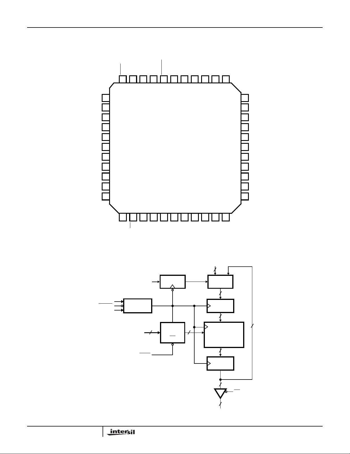
Pinout
HSP9501
44 LEAD PLCC
TOP VIEW
DO0
DO1
DO2
DO3
DO4
V
CC
GND
DO5
DO6
DO7
DO8
CLKSEL
LCEN
7
8
9
10
11
12
13
14
15
16
17
18 19 20 21 22 23 24 25 26 27 28
OE
DO9
NC
LC0
NC
LC1
CLK EN
LC10
CLK
LC9
LC2
LC8
LC3
LC7
LC4
LC6
LC5
DI9
MODSEL
4065 321444342414
NC
39
DI0
38
DI1
37
DI2
36
DI3
35
DI4
34
V
CC
33
GND
32
DI5
31
DI6
30
DI7
29
DI8
Block Diagram
CLKSEL
CLKEN
CLK
MODSEL
CLOCK
GENERATOR
LC0 -10
LCEN
11
REGISTER
REGISTER
EN
DI 0 -9
10
MUX
10
REGISTER
10
11
PROGRAMMABLE
DELAY RAM
0-1279 DELAYS
10
REGISTER
10
10
DO0-9
10
OE
192
Page 3
HSP9501
Pin Descriptions
NAME PIN NUMBER TYPE DESCRIPTION
V
CC
GND 13, 33 The device ground.
CLK 1 I Input Clock. This clock signal is used to control the datamovementthroughtheprogrammablebuff-
DIO-9 27, 29-32, 35-39 I Data Inputs. This 10-bit input port is used to provide the input data. When MODSEL is low, data
DO0-9 7-11, 14-18 O Data Outputs. This 10-bit port provides the output data from the Internal Delay Registers. Data
LC0-10 20-26, 41-44 I Length Control Inputs. These inputs are used to specify the number of clock cycles of delay be-
LCEN 6 I Length Control Enable. LCEN is used in conjunction with LC0-10 and CLK to load a new length
OE 19 I Output Enable. This input controls the state of the DO0-9 output port. A low on this control line en-
12, 34 The +5V power supply pin. A 0.1µF capacitor between the VCC and GND pin is
recommended.
er. It is also the signal which latches the input data, length control word and mode select. Input
setup and hold times with respect to the clock must be met for proper operation.
on the DI0-9 inputs is latched on the clock edge selected by CLKSEL.
latched into the DI0-9 inputs will appear at the DO0 9 outputs on the Nth clock cycle, where N is
the total delay programmed.
tween the DI0-9 inputs and the DO0-9 outputs. An integer value between 0 and 1279 is placed on
the LC0-10 inputs, and the total delay length (N) programmed is the LC0-10 value plus 2. In order
to properly load an active length control word, the value must be presented to the LC0-10 inputs
and LCEN must be asserted during an active clock edge selected by CLKSEL.
control word. An 11-bit value is loaded on the LC0-10 inputs, LCEN is asserted, and the next selected clock edge will load the new count value. Since this operation is synchronous, LCEN must
meet the specified setup/hold times with respect to CLK for proper operation.
ables the port for output. When OE is high, the output drivers are in the high impedance state. Internal latching or transfer of data is not affected by this input.
MODSEL 40 I Mode Select. This input is used to control the mode of operation of the HSP9501. A low on MOD-
SEL causes the device to latch new data at the DI0-9 inputs on every clock cycle, and operate as
a programmablepipeline register.When MODSEL is high, the HSP9501 is in the recirculate mode,
and will operate as a programmablelength circular buffer.This control signal may be used in a synchronous fashion during device operation, however,care must be taken to ensure the required setup/hold times with respect to CLK are met.
CLKSEL 5 I Clock Select Control. This input is used to determine which edge of the CLK signal is used for con-
trolling all internal events. A low on CLKSEL selects the negative going edge, therefore, all setup,
hold, and output delay times are with respect to the negative edge of CLK. When CLKSEL is high,
the positive going edge is selected and all synchronous timing is with respect to the positive edge
of the CLK signal.
CLKEN 2 I Clock Enable. This control signal can be used to enable or disable the CLK input. When low, the
CLK input is enabled and will operate in a normal fashion. A high on CLKEN will disable the CLK
input and will “hold'' all internal operations and data. This control signal may also be used in a synchronousfashion,however,setup and holdrequirements with respect to CLK must be met for proper device operation. This signal takes effect on the clock following the one that latches it in.
193
Page 4

HSP9501
Functional Description
The HSP9501 is a 10-bit wide programmable length data
buffer. The length of delay is programmable from 2 to 1281
delays in single delay increments.
Data into the delay line may be selected from the data input
bus (DI0-9) or as recirculated output, depending on the state
of the mode select (MODSEL) control input.
Mode Select
The MODSEL control pin selects the source of the data
moving into the delay line. When MODSEL is low, the data
input bus (DI0-9) is the source of the data. When MODSEL
is high, the output of the HSP9501 is routed back to the input
to form a circular buffer.
The MODSEL control line is latched at the input by the CLK
signal. The edge which latches this control signal is determined by the CLKSEL control line. In either case, the
MODSEL line is latched on one edge of the CLK signal with
the following edge moving data into and through the
HSP9501. Refer to the functional timing waveforms for
specific timing references.
Clock Select Logic
The clock select logic is provided to allow the use of positive
or negative edge system clocks. The active edge of the CLK
input to the HSP9501 is controlled through the use of the
CLKSEL input.
When CLKSEL is low, the negative going edge of CLK is
used to control all internal operations. A high on CLKSEL
selects the positive going edge of CLK.
All synchronous timing (i.e., setup, hold and output
propagation delay times are relative to the CLK edge
selected by CLKSEL. Functional timing waveforms for each
state of CLKSEL are provided (refer to Timing Waveforms for
details).
Delay Path Control
The HSP9501 buffer length is programmable from 2to 1281
data words in one word increments. The minimum number of
delays which can be programmed is two, consisting of the
input and Output Buffer Registers only.
The length control inputs (LC0-10) are used to set the length
of the programmable delay ram which can vary in length
from 0 to 1279. The total length of the HSP9501 data buffer
will then be equal to the programmed value on LC0-10 plus
2. The programmed delay is established by the 11-bit integer
value of the LC0-10 inputs with LC-10 as the MSB and LC0
as the LSB.
For example,
LC10 9 8 7 6 5 4 3 2 1 LC0
0 000100000 1
programs a length value of 2
the delay will be 65 + 2 or 67 delays.
Table 1 indicates several programming values. The decimal
value placed on LC0-10 must not exceed 1279. Controlled
operation with larger values is not guaranteed.
Values on LC0-10 are latched on the CLK edge selected by
the CLKSEL control line, when
LCEN must meet the specified setup and hold times relative
to the selected CLK edge for proper device operation.
6
+ 20 = 65. The total length of
LCEN is active. LC0-10 and
TABLE 1. LENGTH CONTROL PROGRAMMING EXAMPLES
TOTAL
LC9
10
LC10 2
0 0000000000 0 2
0 0 0 0 1 1 1 0 1 1 0 118 120
0 1 1 0 0 1 0 1 0 0 0 808 810
1 0 0 0 0 0 1 1 0 0 1 1049 1051
1 0 0 1 1 1 1 1 1 1 1 1279 1281
LS8
9
2
LC7
8
2
LC6
7
2
LC5
6
2
LC4
5
2
LC3
4
2
LC2
3
2
LC1
2
2
LC0
1
2
0
2
PROGRAMMED
LENGTH
LENGTH
194
N
Page 5

HSP9501
Absolute Maximum Ratings Thermal Information
Supply Voltage. . . . . . . . . . . . . . . . . . . . . . . . . . . . . . . . . . . . . +8.0V
Input, Output or Voltage Applied . . . . . . . .GND -0.5V to VCC +0.5V
Operating Conditions
Temperature Range . . . . . . . . . . . . . . . . . . . . . . . . . . . .0oC to 70oC
Voltage Range. . . . . . . . . . . . . . . . . . . . . . . . . . . . +4.75V to 5.25V
CAUTION: Stresses above those listed in “Absolute Maximum Ratings” may cause permanent damage to the device. This is a stress only rating and operationofthe
device at these or any other conditions above those indicated in the operational sections of this specification is not implied.
NOTE:
1. θJA is measured with the component mounted on an evaluation PC board in free air.
Thermal Resistance (Typical, Note 1) θJA (oC/W)
PLCC Package. . . . . . . . . . . . . . . . . . . . . . . . . . . . . 45.2
Maximum Junction Temperature . . . . . . . . . . . . . . . . . . . . . . .150oC
Maximum Storage Temperature Range. . . . . . . . . . -65oC to 150oC
Maximum Lead Temperature (Soldering 10s) . . . . . . . . . . . . .300oC
(PLCC - Lead Tips Only)
DC Electrical Specifications V
= 5.0V +5%, TA = 0oC to 70oC, Commercial
CC
PARAMETER SYMBOL TEST CONDITIONS MIN MAX UNITS
Logical One Input Voltage V
Logical Zero Input Voltage V
Output HIGH Voltage V
Output LOW Voltage V
Input Leakage Current I
Output Leakage Current I
Standby Current I
Operating Power Supply Current I
Input Capacitance C
Output Capacitance C
AC Electrical Specifications V
= 5.0V ±5%, TA = 0oC to +70oC, Commercial, (Note 5)
CC
PARAMETER SYMBOL
Clock Period t
Clock Pulse Width High t
Clock Pulse Width Low t
Data Input Setup Time t
Data Input Hold Time t
Output Enable Time t
Output Disable Time t
CLKEN to Clock Setup t
CLKEN to Clock Hold t
LC0-10 Setup Time t
LC0-10 Hold Time t
LCEN to Clock Setup t
LCEN to Clock Hold t
IH
IL
OH
OL
I
O
CCSB
CCOP
IN
O
CP
PWH
PWL
DS
DH
ENA
DIS
ES
EH
LS
LH
LES
LEH
VCC = 5.25V 2.0 - V
VCC = 4.75V - 0.8 V
IOH = -4mA VCC = 4.75V 2.4 - V
IOL = +4.0mA VCC = 4.75V - 0.4 V
VIN = GND or VCC VCC = 5.25V -10 10 µA
V
= GND or VCC = 5.25V -10 10 µA
OUT
VIN = VCC or GND, VCC = 5.25V, Note 3 - 500 µA
f = 25MHz, VIN = VCC or GND
- 125 mA
VCC = 5.25V, Notes 2, 3
FREQ = 1MHz, VCC = Open, All
-10 pF
measurements are referenced to device
GND
-10 pF
-32 -25
UNITS NOTESMIN MAX MIN MAX
31 - 40 - ns 12 - 15 - ns 12 - - 15 ns 10 - 12 - ns -
2-2-ns-
- 20 - 25 ns -
- 24 - 25 ns Note 4
10 - 12 - ns -
2-2-ns-
10 - 13 - ns -
2-2-ns-
10 - 13 - ns -
2-2-ns-
195
Page 6

HSP9501
AC Electrical Specifications V
= 5.0V ±5%, TA = 0oC to +70oC, Commercial, (Note 5) (Continued)
CC
-32 -25
PARAMETER SYMBOL
MODSEL Setup Time t
MODSEL Hold Time t
Clock to Data Out T
Output Hold from Clock T
Rise, Fall Time T
MS
MH
OUT
OH
RF
10 - 13 - ns -
2-2-ns-
- 16 - 22 ns -
4-4-ns-
-6-6nsNote 4
UNITS NOTESMIN MAX MIN MAX
NOTES:
2. Power supply current is proportional to operating frequency. Typical rating for I
CCOP
is 5mA/MHz.
3. Output load per test load circuit with switch open and CL = 40pF.
4. Controlled by design or process parameters and not directly tested. Characterized upon initial design and after major process and/or design
changes.
5. AC Testing is performed as follows: Input levels: 0V and 3.0V, timing reference levels = 1.5V, input rise and fall times driven at 1ns/V, output
load CL = 40pF.
Test Load Circuit
SWITCH S1 OPEN FOR I
NOTE: Includes stray and jig capacitance.
DUT
CCSB
C
L
AND I
S
1
(NOTE)
CCOP
±
I
OH
EQUIVALENT CIRCUIT
1.5V I
OL
196
Page 7

Timing Waveforms
CLK
MODSEL
HSP9501
t
CP
t
t
MS
PWH
t
PWL
t
MH
DI 0 -9
OE
DO 0 -9
CLKEN
INTERNAL
CLOCK
CLK
t
OUT
t
DH
t
DIS
t
DS
t
OH
FIGURE 1. FUNCTIONAL TIMING (CLKSEL = LOW)
t
ES
T
EH
t
ES
FIGURE 2. CLEN TIMING (CLKSEL = LOW)
1.3
1.7
t
ENA
CLK
t
2.0V
0.8V
t
RF
2.0V
0.8V
LCEN
t
RF
LC0 -10
LES
t
LS
t
LEH
t
LH
FIGURE 3. OUTPUT RISE AND FALL TIMES FIGURE 4. LENGTH CONTROL TIMING (CLKSEL = LOW)
197
Page 8

HSP9501
Timing Waveforms
CLK
MODSEL
DI 0 -9
OE
DO 0 -9
CLK
CLKEN
(Continued)
t
MS
t
CP
t
PWL
t
DS
t
OH
t
OUT
t
PWH
t
DH
t
DIS
FIGURE 5. FUNCTIONAL TIMING (CLKSEL = HIGH)
t
ES
t
EH
t
ES
1.7
1.3
t
ENA
t
MH
INTERNAL
CLOCK
FIGURE 6. CLKEN TIMING (CLKSEL = HIGH)
CLK
LCEN
LC 0 -10
t
LES
t
LS
t
LEH
t
LH
FIGURE 7. LENGTH CONTROL TIMING (CLKSEL = HIGH)
All Intersil semiconductor products are manufactured, assembled and tested under ISO9000 quality systems certification.
Intersil semiconductor products are sold by description only. Intersil Corporation reserves the right to make changes in circuit design and/or specifications at any time without notice. Accordingly, the reader is cautioned to verify that data sheets are current before placing orders. Information furnished by Intersil is believed to be accurate and
reliable. However ,no responsibility is assumed by Intersil or its subsidiaries for its use; nor for any infringements of patents or other rights of third parties which may result
from its use. No license is granted by implication or otherwise under any patent or patent rights of Intersil or its subsidiaries.
For information regarding Intersil Corporation and its products, see web site http://www.intersil.com
198
 Loading...