

Page 1
HSP50215EVAL
User’s Manual January 1999 File Number
DSP Modulator Evaluation Board
Evaluation Kit
The HSP50215EVAL Kit provides the necessary tools to
evaluate the HSP50215 Digital Upconverter integrated
circuit and consists of a circuit board and a software
program. The kit is designed for evaluation of Digital
Quadrature Amplitude, FM, and Shaped FM modulation for
IF Communications Applications. The circuit board uses
baseband I and Q data patterns loaded through the 8-bit
parallel interface or the ISAbus interface. Data is output as
either a digital or analog modulated composite IF signal. Up
to four channels can be included in the composite IF output.
To facilitate the use of the board during evaluation, the kit
includes example files for configuration, shaping filters and
input stimulus.
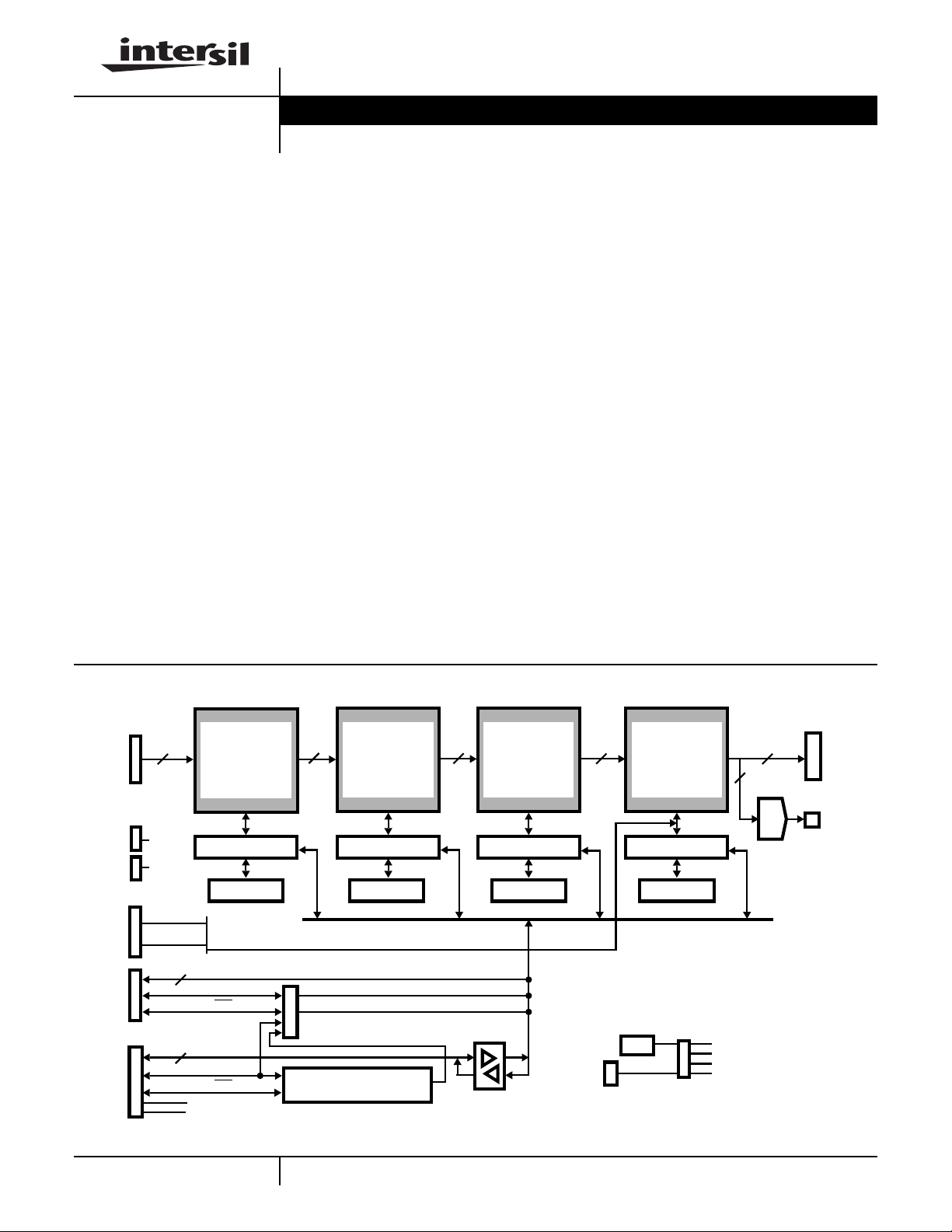
Circuit Board
The Functional BlockDiagram illustrates the major functions
of the circuit board. The circuit board is a ISAbus form factor
with 40 pin I/O header/connectors for cascade and output
signals. Baseband test patterns are loaded through the
ISAbus or 8-bit parallel interface. The external Cascade
Input allows expansion of the number of channels in the
composite signal. The board outputs data through both the
RF connector and the 40 pin header. Test connectors are
provided at key signal and control locations in the circuit.
4463.3
Features
• Multi-Channel Composite IF Output with 1-4 Channels
• Digital or Analog Composite Output
• Baseband Pattern Stimulus Files with Lengths to 64Kbits
• Example Baseband Patterns for BPSK, QPSK,
π/4QPSK,
16QAM, FM, GMSK and AWG Noise
• Baseband Patterns Loaded to RAM Via PC ISAbus or
Parallel Port, for Use as Modulator Baseband Data
• DOS Based Configuration/Status Software
Applications
• Evaluation Tool for the Performance of the Digital
UpConverter Configured as PSK, Quadrature Amplitude
(QAM), FM and Shaped FM (MSK) Modulators at Rates
from <1 KBPS to 1.5 MBPS
• Performance Evaluation Tool for Digital Upconversion
• Communications Test Equipment
Functional Block Diagram
40 PIN
CONNECTOR
16 16 16
(CASCADE
INPUT)
V
CC
-12V
DAT A
ADDRESS
8
PARALLEL
8
ISABUS
HSP50215
DIGITAL
UPCONVERTER
CHANNEL 4
FPGA
RAM
(INPUT DATA PATH AND CONTROL/STATUS INTERFACE)
(OPTIONAL FINAL STAGE BASEBAND DATA INPUT PATH)
DAT A
ADDRESS
WR
DAT A
ADDRESS
WR
V
CC
-12V
HSP50215
DIGITAL
UPCONVERTER
CHANNEL 3
FPGA FPGA FPGA
RAM RAM RAM
ADDRESS DECODE
HSP50215
DIGITAL
UPCONVERTER
CHANNEL 2
INTERFACE BUS
16
CLK
HSP50215
DIGITAL
UPCONVERTER
CHANNEL 1
OSC
16
14
D/A
HI5741
INTERNAL
CLOCKS
40 PIN
CONNECTOR
DIGITAL
ANALOG
IF OUTPUT
IF OUTPUT
1
CAUTION: These devices are sensitive to electrostatic discharge; follow proper IC Handling Procedures.
http://www.intersil.com or 407-727-9207
| Copyright © Intersil Corporation 1999
Page 2

HSP50215EVAL
Table of Contents
Functional Block Diagram. . . . . . . . . . . . . . . . . . . . . . . . . . . . . . . . . . . . . . . . . . . . . . . . . . . . . . . . . . . . . . . . . . . . . . . . . . . . . . . . . . . . . . . . 1
Control Software Program . . . . . . . . . . . . . . . . . . . . . . . . . . . . . . . . . . . . . . . . . . . . . . . . . . . . . . . . . . . . . . . . . . . . . . . . . . . . . . . . . . . . . . . 3
FIGURE 1. MENU TREE FOR THE CONTROL/STATUS SOFTWARE. . . . . . . . . . . . . . . . . . . . . . . . . . . . . . . . . . . . . . . . . . . . . . . . . 3
Configuration/Test Headers . . . . . . . . . . . . . . . . . . . . . . . . . . . . . . . . . . . . . . . . . . . . . . . . . . . . . . . . . . . . . . . . . . . . . . . . . . . . . . . . . . . . . . 4
Typical Evaluation Configuration. . . . . . . . . . . . . . . . . . . . . . . . . . . . . . . . . . . . . . . . . . . . . . . . . . . . . . . . . . . . . . . . . . . . . . . . . . . . . . . . . . 4
Getting Started. . . . . . . . . . . . . . . . . . . . . . . . . . . . . . . . . . . . . . . . . . . . . . . . . . . . . . . . . . . . . . . . . . . . . . . . . . . . . . . . . . . . . . . . . . . . . . . . . 4
Evaluation Circuit Board Configuration and Set Up . . . . . . . . . . . . . . . . . . . . . . . . . . . . . . . . . . . . . . . . . . . . . . . . . . . . . . . . . . . . . . . . . . . 4
Requirements for the Control Software Program . . . . . . . . . . . . . . . . . . . . . . . . . . . . . . . . . . . . . . . . . . . . . . . . . . . . . . . . . . . . . . . . . . . . . 4
Installing the Software . . . . . . . . . . . . . . . . . . . . . . . . . . . . . . . . . . . . . . . . . . . . . . . . . . . . . . . . . . . . . . . . . . . . . . . . . . . . . . . . . . . . . . . . . 4
FIGURE 2. TYPICAL MODULATOR PERFORMANCE EVALUATION CONFIGURATION . . . . . . . . . . . . . . . . . . . . . . . . . . . . . . . . . . 4
Verifying the Control Software and Board Installation . . . . . . . . . . . . . . . . . . . . . . . . . . . . . . . . . . . . . . . . . . . . . . . . . . . . . . . . . . . . . . . . . 5
FIGURE 3. MAIN MENU . . . . . . . . . . . . . . . . . . . . . . . . . . . . . . . . . . . . . . . . . . . . . . . . . . . . . . . . . . . . . . . . . . . . . . . . . . . . . . . . . . . . 5
FIGURE 4. BOARD INTERFACE SUBMENU . . . . . . . . . . . . . . . . . . . . . . . . . . . . . . . . . . . . . . . . . . . . . . . . . . . . . . . . . . . . . . . . . . . . 5
FIGURE 5. TEST SUBMENU. . . . . . . . . . . . . . . . . . . . . . . . . . . . . . . . . . . . . . . . . . . . . . . . . . . . . . . . . . . . . . . . . . . . . . . . . . . . . . . . . 5
Running the Control Software for Evaluation Testing. . . . . . . . . . . . . . . . . . . . . . . . . . . . . . . . . . . . . . . . . . . . . . . . . . . . . . . . . . . . . . . . . . 6
FIGURE 6. MODULATOR CHANNEL CONFIGURATION SUBMENU . . . . . . . . . . . . . . . . . . . . . . . . . . . . . . . . . . . . . . . . . . . . . . . . . 6
FIGURE 7. BOARD INTERFACE SUBMENU . . . . . . . . . . . . . . . . . . . . . . . . . . . . . . . . . . . . . . . . . . . . . . . . . . . . . . . . . . . . . . . . . . . . 6
FIGURE 8. CONFIGURE CHANNEL 1 SUBMENU. . . . . . . . . . . . . . . . . . . . . . . . . . . . . . . . . . . . . . . . . . . . . . . . . . . . . . . . . . . . . . . . 6
Learning Your Way Around. . . . . . . . . . . . . . . . . . . . . . . . . . . . . . . . . . . . . . . . . . . . . . . . . . . . . . . . . . . . . . . . . . . . . . . . . . . . . . . . . . . . . . . 7
Exercise #1: Generating A CW Tone . . . . . . . . . . . . . . . . . . . . . . . . . . . . . . . . . . . . . . . . . . . . . . . . . . . . . . . . . . . . . . . . . . . . . . . . . . . . . . 7
Exercise #2: Adjusting the level of the CW Tone . . . . . . . . . . . . . . . . . . . . . . . . . . . . . . . . . . . . . . . . . . . . . . . . . . . . . . . . . . . . . . . . . . . . . 8
Exercise #3: Modulating the CW Tone with PN Data . . . . . . . . . . . . . . . . . . . . . . . . . . . . . . . . . . . . . . . . . . . . . . . . . . . . . . . . . . . . . . . . . . 8
Exercise #4: CW and a Modulated Signal . . . . . . . . . . . . . . . . . . . . . . . . . . . . . . . . . . . . . . . . . . . . . . . . . . . . . . . . . . . . . . . . . . . . . . . . . . 9
Exercise #5: A Fourier Series Composite Signal . . . . . . . . . . . . . . . . . . . . . . . . . . . . . . . . . . . . . . . . . . . . . . . . . . . . . . . . . . . . . . . . . . . . . 9
Exercise #6: Generating Additive White Gaussian Noise (AWGN) . . . . . . . . . . . . . . . . . . . . . . . . . . . . . . . . . . . . . . . . . . . . . . . . . . . . . . . 9
Background on Eb/No and SNR Calculations . . . . . . . . . . . . . . . . . . . . . . . . . . . . . . . . . . . . . . . . . . . . . . . . . . . . . . . . . . . . . . . . . . . . . . . 10
An Example Eb/No Calculation . . . . . . . . . . . . . . . . . . . . . . . . . . . . . . . . . . . . . . . . . . . . . . . . . . . . . . . . . . . . . . . . . . . . . . . . . . . . . . . . . . 11
Exercise #7: PRBS Data . . . . . . . . . . . . . . . . . . . . . . . . . . . . . . . . . . . . . . . . . . . . . . . . . . . . . . . . . . . . . . . . . . . . . . . . . . . . . . . . . . . . . . . 11
Generating User Configurations. . . . . . . . . . . . . . . . . . . . . . . . . . . . . . . . . . . . . . . . . . . . . . . . . . . . . . . . . . . . . . . . . . . . . . . . . . . . . . . . . . 11
Detailed Circuit Description . . . . . . . . . . . . . . . . . . . . . . . . . . . . . . . . . . . . . . . . . . . . . . . . . . . . . . . . . . . . . . . . . . . . . . . . . . . . . . . . . . . . . . 12
Signal Path . . . . . . . . . . . . . . . . . . . . . . . . . . . . . . . . . . . . . . . . . . . . . . . . . . . . . . . . . . . . . . . . . . . . . . . . . . . . . . . . . . . . . . . . . . . . . . . . . . . . 12
Modulation Channel 4. . . . . . . . . . . . . . . . . . . . . . . . . . . . . . . . . . . . . . . . . . . . . . . . . . . . . . . . . . . . . . . . . . . . . . . . . . . . . . . . . . . . . . . . . . 12
Modulation Channel 3. . . . . . . . . . . . . . . . . . . . . . . . . . . . . . . . . . . . . . . . . . . . . . . . . . . . . . . . . . . . . . . . . . . . . . . . . . . . . . . . . . . . . . . . . . 12
Modulation Channel 2. . . . . . . . . . . . . . . . . . . . . . . . . . . . . . . . . . . . . . . . . . . . . . . . . . . . . . . . . . . . . . . . . . . . . . . . . . . . . . . . . . . . . . . . . . 12
Modulation Channel 1. . . . . . . . . . . . . . . . . . . . . . . . . . . . . . . . . . . . . . . . . . . . . . . . . . . . . . . . . . . . . . . . . . . . . . . . . . . . . . . . . . . . . . . . . . 12
PC/Controller Interface Section . . . . . . . . . . . . . . . . . . . . . . . . . . . . . . . . . . . . . . . . . . . . . . . . . . . . . . . . . . . . . . . . . . . . . . . . . . . . . . . . . . . 13
ISA Interface. . . . . . . . . . . . . . . . . . . . . . . . . . . . . . . . . . . . . . . . . . . . . . . . . . . . . . . . . . . . . . . . . . . . . . . . . . . . . . . . . . . . . . . . . . . . . . . . . 13
Parallel Interface Configuration . . . . . . . . . . . . . . . . . . . . . . . . . . . . . . . . . . . . . . . . . . . . . . . . . . . . . . . . . . . . . . . . . . . . . . . . . . . . . . . . . . 13
Clocking . . . . . . . . . . . . . . . . . . . . . . . . . . . . . . . . . . . . . . . . . . . . . . . . . . . . . . . . . . . . . . . . . . . . . . . . . . . . . . . . . . . . . . . . . . . . . . . . . . . . . . 13
Jumpered Options . . . . . . . . . . . . . . . . . . . . . . . . . . . . . . . . . . . . . . . . . . . . . . . . . . . . . . . . . . . . . . . . . . . . . . . . . . . . . . . . . . . . . . . . . . . . 13
Power Supply Connections. . . . . . . . . . . . . . . . . . . . . . . . . . . . . . . . . . . . . . . . . . . . . . . . . . . . . . . . . . . . . . . . . . . . . . . . . . . . . . . . . . . . . . . 13
Advanced Evaluation Configurations . . . . . . . . . . . . . . . . . . . . . . . . . . . . . . . . . . . . . . . . . . . . . . . . . . . . . . . . . . . . . . . . . . . . . . . . . . . . . . 13
Non ISA (PC installed) Operation. . . . . . . . . . . . . . . . . . . . . . . . . . . . . . . . . . . . . . . . . . . . . . . . . . . . . . . . . . . . . . . . . . . . . . . . . . . . . . . . . 13
Direct Modulator Control. . . . . . . . . . . . . . . . . . . . . . . . . . . . . . . . . . . . . . . . . . . . . . . . . . . . . . . . . . . . . . . . . . . . . . . . . . . . . . . . . . . . . . . . 14
Using SERINADE™ Designed Filters . . . . . . . . . . . . . . . . . . . . . . . . . . . . . . . . . . . . . . . . . . . . . . . . . . . . . . . . . . . . . . . . . . . . . . . . . . . . . 14
Appendix A - Circuit Board Layout . . . . . . . . . . . . . . . . . . . . . . . . . . . . . . . . . . . . . . . . . . . . . . . . . . . . . . . . . . . . . . . . . . . . . . . . . . . . . . . . 14
Appendix B - Initial Jumper Settings. . . . . . . . . . . . . . . . . . . . . . . . . . . . . . . . . . . . . . . . . . . . . . . . . . . . . . . . . . . . . . . . . . . . . . . . . . . . . . . 15
Appendix C - Connector Pin Assignments . . . . . . . . . . . . . . . . . . . . . . . . . . . . . . . . . . . . . . . . . . . . . . . . . . . . . . . . . . . . . . . . . . . . . . . . . . 17
Appendix D - Test Header Pin Assignments. . . . . . . . . . . . . . . . . . . . . . . . . . . . . . . . . . . . . . . . . . . . . . . . . . . . . . . . . . . . . . . . . . . . . . . . . 19
Appendix E - Detailed Schematics. . . . . . . . . . . . . . . . . . . . . . . . . . . . . . . . . . . . . . . . . . . . . . . . . . . . . . . . . . . . . . . . . . . . . . . . . . . . . . . . . 22
Appendix F - Parts List . . . . . . . . . . . . . . . . . . . . . . . . . . . . . . . . . . . . . . . . . . . . . . . . . . . . . . . . . . . . . . . . . . . . . . . . . . . . . . . . . . . . . . . . . . 34
Appendix G - Descriptive File List . . . . . . . . . . . . . . . . . . . . . . . . . . . . . . . . . . . . . . . . . . . . . . . . . . . . . . . . . . . . . . . . . . . . . . . . . . . . . . . . . 35
Example Configuration Files . . . . . . . . . . . . . . . . . . . . . . . . . . . . . . . . . . . . . . . . . . . . . . . . . . . . . . . . . . . . . . . . . . . . . . . . . . . . . . . . . . . . . 35
Example Filter Files. . . . . . . . . . . . . . . . . . . . . . . . . . . . . . . . . . . . . . . . . . . . . . . . . . . . . . . . . . . . . . . . . . . . . . . . . . . . . . . . . . . . . . . . . . . . . 37
FIGURE 9. IS136B.IMP FREQUENCY RESPONSE. . . . . . . . . . . . . . . . . . . . . . . . . . . . . . . . . . . . . . . . . . . . . . . . . . . . . . . . . . . . . . . 38
FIGURE 10. RRC2A4X.IMP FREQUENCY RESPONSE . . . . . . . . . . . . . . . . . . . . . . . . . . . . . . . . . . . . . . . . . . . . . . . . . . . . . . . . . . . 38
FIGURE 11. GS5T16X.IMP FREQUENCY RESPONSE. . . . . . . . . . . . . . . . . . . . . . . . . . . . . . . . . . . . . . . . . . . . . . . . . . . . . . . . . . . . 39
FIGURE 12. S95MOD.IMP FREQUENCY RESPONSE . . . . . . . . . . . . . . . . . . . . . . . . . . . . . . . . . . . . . . . . . . . . . . . . . . . . . . . . . . . . 39
FIGURE 13. AMPS2.IMP FREQUENCY RESPONSE. . . . . . . . . . . . . . . . . . . . . . . . . . . . . . . . . . . . . . . . . . . . . . . . . . . . . . . . . . . . . . 40
FIGURE 14. RRC35A4X.IMP FREQUENCY RESPONSE . . . . . . . . . . . . . . . . . . . . . . . . . . . . . . . . . . . . . . . . . . . . . . . . . . . . . . . . . . 40
FIGURE 15. GP1.IMP FREQUENCY RESPONSE . . . . . . . . . . . . . . . . . . . . . . . . . . . . . . . . . . . . . . . . . . . . . . . . . . . . . . . . . . . . . . . . 41
FIGURE 16. GP2.IMP FREQUENCY RESPONSE . . . . . . . . . . . . . . . . . . . . . . . . . . . . . . . . . . . . . . . . . . . . . . . . . . . . . . . . . . . . . . . . 41
Example Stimulus Files. . . . . . . . . . . . . . . . . . . . . . . . . . . . . . . . . . . . . . . . . . . . . . . . . . . . . . . . . . . . . . . . . . . . . . . . . . . . . . . . . . . . . . . . . . 42
Appendix H - Detailed Menu Item Descriptions . . . . . . . . . . . . . . . . . . . . . . . . . . . . . . . . . . . . . . . . . . . . . . . . . . . . . . . . . . . . . . . . . . . . . . 43
PAGE
2
Page 3
HSP50215EVAL
Control Software Program
The control software program, written for DOS based PC’ s , is
included in the evaluation kit. This software supports operation
of the evaluation circuit board in basic quadrature ASK and FM
modulation configurations
The control software MAIN MENU offers six submenus f or
various configuration selections and three command actions.
The menu tree is illustrated in Figure 1.
The 7 configuration submenus are:
• Board Configuration Menu
• Modulator Channel 1 Configuration Menu
• Modulator Channel 2 Configuration Menu
• Modulator Channel 3 Configuration Menu
• Modulator Channel 4 Configuration Menu
• Configure Board Menu
• Test Menu
The four command actions are:
• Load Configuration File
• Save Configuration File
• Compute Registers
• Exit
A typical operational sequence is:
A. Load Configuration File
Executing MAIN MENU item (5) brings up a screen with the
current file name and requests the name of the file to be
loaded. Once the new file name is entered, this command
loads the configuration setup and returns to the MAIN MENU
screen. This command allows the user to select a previously
saved configuration file f or displa y, revie w and editing.
B. Edit Configuration File
This is done by sequencing through each of the configuration
submenus and adjusting the parameters for the desired
hardware configuration.
- The BOARD CONFIGURATION MENU is used to select
control interface type, printer port (PRN) number, FPGA
addressing, and oscillator frequency.
- The MODULA TOR CHANNEL CONFIGURA TION
MENUS are used to select carrier center frequency , input
sample rate, modulation type, coefficient file name,
interpolation factor, impulse response length, Stimulus file
name, number of data samples, output attenuation, output
enabling, cascade input control, synchronization,
synchronization polarity , FIFO depth, Output F ormat, and
test register settings. There is a menu for each of the f our
modulator channels on the evaluation board.
C. Save Configuration File
Executing MAIN MENU item (6) brings up a screen with the
current file name and a request for a file name to be saved.
Once the new file name is entered, this command stores the
configuration setup to the new file.
WARNING: Failure to change the .cfg file name may result in overwriting of
an example file with an edited version of that file.
D. Compute Registers
This command will use the configuration data entered in MAIN
menu items 0-4, and generate a number of files which contain
the register values for the IC’s on the evaluation circuit board.
The computation is based on a .cfg file, which contains filter
(.imp) and stimulus (.imp) files for each of the 4 channels.The
computed register values are stored in a set of files identified by
the suffix of .1, .2, .3 and .4, indicating the channel to which the
parameters apply. The actual filename preceding the .1, .2, .3
or .4 suffix is automatically assigned to be the Configuration file
filename.
MAIN MENU
(5) LOAD CONFIGURATION FILE
(6) SAVE CONFIGURATION FILE
(0) (1) (2) (3) (4) (8)
BOARD
CONFIGURATION
ENTER
NEW
(1)
VALUE
MENU
ENTER
(7)
NEW
VALUE
MENU
MODULATOR MODULATOR
CHANNEL 1
CONFIGURATION
ENTER
(1) (1)
(16) (16)
NEW
VALUE
MENU
ENTER
NEW
VALUE
MENU
CHANNEL 2
CONFIGURATION
ENTER
NEW
VALUE
MENU
ENTER
NEW
VALUE
MENU
CONFIGURATION
(1)
(16)
(7) COMPUTE REGISTERS
(10) EXIT
MODULATOR
CHANNEL 3
ENTER
NEW
VALUE
MENU
ENTER
NEW
VALUE
MENU
MODULATOR
CHANNEL 4
CONFIGURATION
ENTER
(1)
(16)
NEW
VALUE
MENU
ENTER
NEW
VALUE
MENU
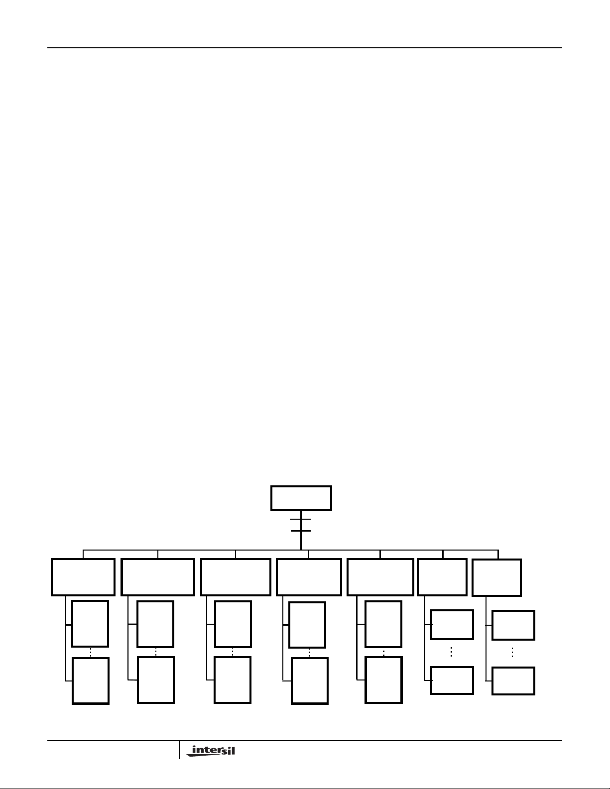
FIGURE 1. MENU TREE FOR THE CONTROL/STATUS SOFTWARE
3
CONFIGURE
BOARD
COMMAND
(1)
COMMAND
(5)
(9)
TEST
COMMAND
(1)
#1
(3)
#2
#1
COMMAND
#2
Page 4
HSP50215EVAL
E. Configure Board Menu
This command accesses a menu called the BOARD,
INTERFACE MENU. The BOARD, INTERFACE MENU is
used to select among several board configure command
options, including configure channel 1, configure channel 2,
configure channel 3, configure channel 4, or configure all
modulator channels.
D. Test Menu
This command accesses a menu called the TEST MENU.
The TEST MENU is used to select among several “run”
options, including reset the board, write to a location while
reset, read to a location while reset, write to a location while
running, or read from a location while running.
For a detailed listing of every Menu screen, with selection
item definitions, refer to Appendix G - Descriptive File List.
Configuration/Test Headers
Fifteen dual row test headers located on the evaluation circuit
board are used to monitor signals and set control pins. The
pin assignments for each of these headers are found in
Appendix D - Test Header Pin Assignments.
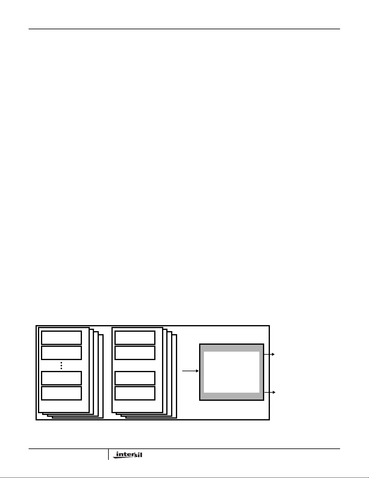
Typical Evaluation Configuration
Figure 2 identifies the configuration of a typical performance
evaluation setup. A test PRBS data pattern is created via a
stimulus file and used by a modulator to generate a
modulated IF signal. Noise and other signal impairment
stimulus files can be used with additional channels to create
a cascaded/summed composite IF signal that is routed to a
D/A converter (DAC), generating an output analog signal.
The digitized IF signal is also routed out of the circuit board
allowing multiple boards to be cascaded together. To check
out a complete communication systems, the modulator
output can be routed to a demodulator, whose baseband
output is connected to a Bit Error Rate Tester (BERT) for
measuring the Bit Error Rate (BER) performance.
Getting Started
Evaluation Circuit Board Configuration and Set Up
1. ___ Power down the host PC and remove the cover to allow access to the motherboard empty slots.
2. ___ Review the jumper configuration of the
HSP50215EVAL Board to verify that the jumpers are
properly set for the configuration desired. Appendices
B (especially the jumper diagram at the end of the appendix), D and E will be helpful in this verification.
3. ___ Install the HSP50215EVALintoone of the empty ISA
slots on the host PC motherboard. Make sure that a
good connection is made with the motherboard and
that the connectors fit in the slots in the rear of the PC
chassis properly. Record the oscillator frequency for
future reference: ____ ____ ____Hz
4. ___ Re-install the PC chassis cover and power up the
computer.
The circuit board is ready for use.
Requirements for the Control Software Program
In order to properly operate the HSP50215EVAL Control
Software Program included in the evaluation kit, the PC must
meet the following requirements:
PC/XT/AT or 100% compatible with a minimum of 640K of
RAM
DOS Version 3.0 or higher.
One parallel port with 25 pin connector.
Installing the Software
The instructions that follow will load both the
HSP50215EVAL software onto the “C” driveof the computer.
If you do not wish to run the software from the “C” drive,
consult your computer user’s manual for operation from
another drive. It is “good practice” to backup original disks
prior to installing the software on your computer.
1. ___ Insert the HSP50215EVALdistribution disk in DriveA
and copy the contents of the distribution diskette to the
targetdirectory on DriveC.
a way as to retain the file structure of the distribution disk.
Note: Thismust be donein such
CHANNEL #1
STIMULUS FILE
CHANNEL #1
FILTER FILE
CHANNEL #4
STIMULUS FILE
CHANNEL #4
FILTER FILE
CONFIGURATION FILE
CHANNEL #1
STIMULUS FILE
CHANNEL #1
FILTER FILE
CHANNEL #4
STIMULUS FILE
CHANNEL #4
FILTER FILE
CONFIGURATION FILE
FIGURE 2. TYPICAL MODULATOR PERFORMANCE EVALUATION CONFIGURATION
PERSONAL COMPUTER
HSP50215EVAL
EVALUATION BOARD
4
ANALOG IF OUTPUT
DIGITAL IF OUTPUT
Page 5

HSP50215EVAL
2. ___ If a FIR filter design software tool is desired, then
downloading SERINADE from the Intersil Corporation website into the target directory is recommended. The web site is found at www.intersil.com and
SERINADE is found under the Products column of
the home page. Select
Products Listing
ment Tools
menu item. Select the
Digital Signal Processing
menu item. Select the
SERINADE
Develop-
menu
item. Download of SERINADE can be done from this
location.
The software must be run from the new target directory
established on the C drive.
Verifying the Control Software and Board Installation
1. ___ On the PC, change the directory to the target directory where the control software has been installed.
2. ___ Start the program by typing: HSP50215 <Enter>.
3. ___ The MAIN MENU screen will appear. It will look like
Figure 3.
+------------------------------------+
| HSP50215 EVALUATION BOARD SOFTWARE |
+------------------------------------+
MAIN MENU
(0) Board Configuration
(1) Modulator Channel 1 Configuration
(2) Modulator Channel 2 Configuration
(3) Modulator Channel 3 Configuration
(4) Modulator Channel 4 Configuration
(5) Load Configuration File
(6) Save Configuration File
(7) Compute Registers
(8) Configure Board
(9) Test Menu
(10) Exit
ENTER SELECTION: =
(C) Intersil Corporation 1997 Version 1.0
FIGURE 3. MAIN MENU
4. ___ Select item (0) for board configuration and type <Enter>. The BOARD INTERFACEMENU will appear as
shownin Figure 4. Use the menu items to change the
default board configuration to match the ev aluation
board interface, printer, FPGA addressing and oscillator frequency that you desire. Verify that these settings match the jumper configuration of your
evaluation board.
5. ___ Whenyouhavecompleted makingyourmodifications,
selectitem (0) and type <Enter> to returnto the MAIN
MENU.
6. ___ Select Main Menu item (9) and type <Enter> to enter
the Test Menu. The Test Menu is shown in Figure 5.
7. ___ Select Test Menu Item (6) and type <Enter> to enter
the Test Board submenu.
8. ___ A screenappearsthat indicatestheRAMAddress/Data Bus test results and the HSP50215 data bus test
results.Ifalltheitemshavepassedthetest,theboard
and software have been properly installed and you
are ready to begin evaluation testing. Skip to step 12.
If any test failed, proceed to step 9.
9. ___ If one of the tests shown on the screen for step 8 did
not pass, then the board jumper configuration should
be reviewed, as it is the most lik ely culprit.
+-------------------------------------+
| HSP50215 EVALUATION BOARD SOFTWARE |
+------------------------------------+
BOARD INTERFACE MENU
File Name ................ EXAMPLES\EX01QPSK
(1) Interface ...................... ISA
(2) ISA Base Address ............... 0x300
(3) Channel 1 FPGA Address ......... 0
(4) Channel 2 FPGA Address ......... 1
(5) Channel 3 FPGA Address ......... 2
(6) Channel 4 FPGA Address ......... 3
(7) Oscillator Freq ........... 50000000 Hz
(0) Main Menu
ENTER SELECTION:
(C) Intersil Corporation 1997 Version 1.0
FIGURE 4. BOARD INTERFACE SUBMENU
+------------------------------------+
| HSP50215 EVALUATION BOARD SOFTWARE |
+------------------------------------+
TEST MENU
File Name................... EXAMPLES\EX01QPSK
(1) Reset Board
(2) Write to Location While Reset
(3) Read from Location While Reset
(4) Write to Location While Running
(5) Read from Location While Running
(6) Test Board
(0) Main Menu
ENTER SELECTION:
(C) Intersil Corporation 1997 Version 1.0
FIGURE 5. TEST SUBMENU
10. ___ Next, the physicalinstallation should be checked.
11. ___ If the board is properly installed, then a verify that no
ISAbus card addressing contention exists. Steps 9,
10, AND 11 are the leading causes of board test failure.
5
Page 6

HSP50215EVAL
Running the Control Software for Evaluation
Testing
12. ___ From the MAIN MENU, select the first MODULATOR
CONFIGURATION MENU, item (1), by typing: 1<Enter>. The MODULATOR CHANNEL 1 CONFIGURATION MENU will appear. It should match the entry
found in Figure 6.
13. ___ Make any adjustments to the parameters by entering
the desired item number for parameter selection and
editing each item via the respective parameter entry
submenu. When editing is complete, select item (0)
and type <Enter> to return to the MAIN MENU.
+------------------------------------+
| HSP50215 EVALUATION BOARD SOFTWARE |
+------------------------------------+
File Name............. EXAMPLES\EXO1QPSK
Channel 1
(1) Carrier Center Freq....... 5000000 Hz
(2) Input Sample Rate......... 24300 Hz
(3) Modulation Type........... QASK
(4) Coef File.............. FILTERS\ISA135B
(5) Interpolation (IP)........ 16 phase
(6) Impulse Response Length (DS).16 samples
(7) Stimulus File......... STIMULUS\QPSKPN
(8) # Data Samples:........... 1022
(9) Output Attenuation........ +15dB
(10) Output.................... Enabled
(11) Cascade Input............. Enabled
(12) Sync...................... Internal
(13) Sync Polarity............. L -> H
(14) FIFO Depth................ 3
(15) Output Format........... Offset Binary
(16) Test Register............. 0
(0) Main Menu
ENTER SELECTION:
17. ___ Select MAIN MENU item (8) by typing 8 <Enter>. The
BoardInterfaceMenuwillappearasshowninFigure 7.
18. ___ If youhaveidentifiedmore than one channel for operation, selection of menu item (5) will load all the channels with one command. See step 25 for this action.
In testing, there are times when most of the channels
will remain the same and one channel or one channel
input will change. Menu items (1) through (4) are for
selective channel or channel input configuration. Select the menu item (1), CONFIGURE CHANNEL 1
MENU, of the BOARD INTERFACE MENU by typing
1<Enter>. A menu will appear with three execution
options, as shown in Figure 8. This is the same menu
that will appear when BOARD INTERFACE MENU
items (2) through (5) are selected.
+------------------------------------+
| HSP50215 EVALUATION BOARD SOFTWARE |
+------------------------------------+
BOARD INTERFACE MENU
File Name................... EXAMPLES\EXO1QPSK
(1) Configure Channel 1
(2) Configure Channel 2
(3) Configure Channel 3
(4) Configure Channel 4
(5) Configure All Channels
(0) Main Menu
ENTER SELECTION:
(C) Intersil Corporation 1997 Version 1.0
(C) Intersil Corporation 1997 Version 1.0
FIGURE 6. MODULATOR CHANNEL CONFIGURATION SUB-
MENU
14. ___ Repeat Steps 12 and 13 for MAIN MENU items (2),
(3), and (4). These submenus control Modulator
Channels 2 through 4. These submenus are identical
to those found under MAIN MENU (1) with the exception of the Channel Number and the names of the coefficient file, and stimulus file.
15. ___ Select MAIN MENU item (6) by typing 6 <Enter>.
This will save the edited configuration file. Y ou are
prompted for a file name for your new configuration.
WARNING: Failure to change the .cfg file name may result in
overwriting of an example file with an edited version of that file.
16. ___ Select MAIN MENU item (7) by typing 7<Enter>. This
will compute the configuration register values and
generatethe.1, .2, .3, and .4 files. (Filter and stimulus
files with .imp file extensions must be created prior to
running the HSP50215EVAL software - See Appendix G - Descriptive File List) Note that MAIN MENU
items 1 through 7 can be executedwithout the evaluation circuit board installed.
FIGURE 7. BOARD INTERFACE SUBMENU
19. ___ Select the desired action from the three choices in
(1) Modulator
(2) Pattern RAM
(3) Both
ENTER NEW VALUE [1]:
FIGURE 8. CONFIGURE CHANNEL 1 SUBMENU
the BOARD INTERFACE submenu. The MODULATOR item does an initialization of the designated
channeland begins normal operation of that channel.
The PA TTERN RAM menu item allows individual
STIMULUS files to be downloaded. Selecting item
(3), allows both channel and stimulus configuration
with one command. Selection of an item will return
the user to the BOARD INTERFACE submenu.
20. ___ Items (2), (3), and (4) of the BOARD INTERFACE
submenu, configure only channel 2, 3, and 4 on the
board, respectively. Configure these channels and
return to the main BOARD INTERFACE submenu.
6
Page 7

HSP50215EVAL
21. ___ Item (5) of the main BOARD INTERFACE submenu
does a full initialization and configuration of all four
channels on the board. Item (5) should be selected
wheneverthe board has been reset. After that, items
(2), (3) or (4) can be selected for a faster update.
22. ___ Select HARDWARE INTERFACE submenu item (0)
by typing 0 <Enter>. This returns the user to the
MAIN MENU. You have now configured your board
for its first test configuration. Youmaylook at the output with a scope or spectrum analyzer to verify that
the board is operating as desired.
23. ___ If the output is not as expected, review the configuration of all of the channels to be sure that you have
properly selected the stimulus, filtering and configuration.
24. ___ When designing a newconfigurationsornewstimulus,
it is best to begin by editing the example file that most
closely matches the desired signal or configuration.
Learning Your Way Around
This Section provides a step by step walk through of some
exercises to familiarize the user with the software screens
and the techniques used to generate a variety of stimulus
and configurations of the HSP50215EVAL Board. If the DAC
output is routed to a scope or a spectrum analyzer, then a
visual verification can be made of the configuration changes.
Note that these exercises assume that the concluding
configuration of the previous exercise is the configuration of
the board at the start of the next exercise. The first exercise
configures all channels to ensure success.
Exercise #1: Generating A CW Tone
This exercise will demonstrate the creation of a CW test
tone. The purpose of this exercise is to illustrate the
generation of a signal that is useful in a variety of testing
configurations.
Go to the main menu. Select Item (5), Load Configuration
File, and enter the following file name and path:
examples/ex01qpsk <Enter). Select Item (1), Modulator
Channel 1 Configuration, and enter the following
parameters:
(1)500,000Hz
(2)50,000Hz
(3)QASK
(7)Stimulus\bpskpn
Note: If you have not properly identified the stimulus file or the path to
that file, then the program will not download when you command the
software to configure the board, and will return you to the DOS prompt
at which point you will need to restart the control software and start
from scratch on the configuration.
(8)1
(9)3
(0)Returns to main menu
This configures channel one input stimulus to be a single bit,
sampled at 50kHz, and applied to a 500kHz QASK modulator
(See note below before leaving this item).
with 3dB attenuation. The filter has a data span of 16 samples
and 16 interpolation phases, and is referenced by the filter
filename IS136B. Notice that it was setting item (8) to 1 that
repeatedly sent a single bit to the modulator, creating the CW.
Select main menu item (2) and set the following parameters:
(1)250,000Hz
(2)25,000Hz
(3)QASK
(7)Stimulus\bpskpn
Note: If you have not properly identified the stimulus file or the path to
that file, then the program will not download when you command the
software to configure the board, and will return you to the DOS prompt
at which point you will need to restart the control software and start
from scratch on the configuration.
(See note below before entering this item)
(8)511
(9)48
(0)Returns to main menu
This configures channel two to be a 25Kbps PSK modulator
at 250kHz, but with the RF severely attenuated so as to be
effectively turned off. The IS136B filter is used here, as well
as in Channel 1.
Select main menu item (3) and set the following parameters:
(1)750,000Hz
(2)75,000Hz
(3)QASK
(7)Stimulus\bpskpn
Note: If you have not properly identified the stimulus file or the path to
that file, then the program will not download when you command the
software to configure the board, and will return you to the DOS prompt
at which point you will need to restart the control software and start
from scratch on the configuration.
(See note below before leaving this item).
(8)511
(9)48
(0)Returns to main menu
This configures channel three to be a 75Kbps PSK
modulator at 750kHz, but with the RF severely attenuated so
as to be effectively turned off. Once again, the IS136B filter
is used.
Select Item (4) and set the following parameters:
(1)500,000Hz
(2)501,000Hz
(3)QASK
(5)0
(6)4
(7)Stimulus\gn16k
Note: If you have not properly identified the stimulus file or the path to
that file, then the program will not download when you command the
software to configure the board, and will return you to the DOS prompt
at which point you will need to restart the control software and start
from scratch on the configuration.
(See note below before leaving this item)
7
Page 8

HSP50215EVAL
(8)16384
(9)48
(0)Returns to main menu
This configures channel four to be a 351Kbps PSK
modulator at 500kHz with a Gaussian White Noise input and
with the RF severely attenuated so as to be effectively
turned off.
Select main menu item (6), save configuration file and enter
the following file name and path: examples/exercise.
Select main menu (7) to compute the register values.
Select main menu (8) to configure the board.
Select submenu item (5) to configure all channels.
Select submenu item (3) to load both the modulator and
Pattern RAM.
When the submenu reappears, the download is complete
and the scope or spectrum analyzer should show a single
CW tone at 500kHz at approximately 0.4Vpp.
Exercise #2: Adjusting the level of the CW Tone
This exercise will demonstrate the technique used in
adjusting the output amplitude of the CW test tone via the
Gain Control signal of the Digital Upconverter. This is but
one technique that can be used to set the level, noting that
scaling the input file can achieve the same result. The
HSP50215 data sheet notes that care must be taken in
setting the signal levelat the input to the shaping filter, at the
input to the interpolation filter, at the input to the mixer, and
at the cascade summer. Attention to these points will
eliminate the unwanted limiting or roll-over. The purpose of
this exercise is to introduce the user to a technique for
setting test signal levels.
Go to the main menu. Select Item (1), Modulator Channel 1
Configuration, and enter the following parameters:
(9)9
(0)Returns to main menu
This will reduce the output level by 6dB.
Select main menu (7) to compute the register values.
Select main menu (8) to configure the board.
Select submenu item (1) to configure channel 1.
Select submenu item (1) to load the modulator.
When the submenu reappears, the download is complete
and the scope or spectrum analyzer should show a single
CW tone at 500kHz at with half the amplitude of the signal in
Exercise 1. Note that if we had set the value to 48, the
channel is effectively turned off. Setting the value to 0 is the
maximum output level, but there is the risk that clipping will
occur when other signals are added into the CW tone.
Exercise #3: Modulating the CW Tone with PN Data
This exercise will demonstrate the creation a BPSK signal
using a Random PN sequence as a stimulus. The BPSK
stimulus will write the following values as (I,Q) pairs into the
modulator: (-0.707, -0.707), (+0.707, +0.707). This will
generate a BPSK signal. The purist may wish to edit this file
to have the values (+1,0), (-1,0), but the 45
not of concern, in general. The purpose of this exercise is to
demonstrate BPSK and provide insight into creating useful
test stimulus files, as well as to learn techniques for quick
test configuration.
Go to the main menu. Select Item (1) and set the following
parameters:
(8)24
(9)3
(0)Returns to main menu
This will return the output level to the original setting.
Select main menu (7) to compute the register values.
Select main menu (8) to configure the board.
Select submenu item (1) to configure channel 1.
Select submenu item (1) to load the modulator.
When the submenu reappears, the download is complete
and the scope or spectrum analyzer should show a filtered,
modulated signal at an output levelof approximately 0.4Vpp.
There should be 10 IF cycles per baud and the baud rate is
50kHz. Notice that it was setting item (8) to 24 that sent a PN
sequence to the modulator. The previous value of 1, held the
modulator at CW using an input of either a (-0.707, -0.707)
or (+0.707, +0.707).
Note that if a particular data pattern is required, copying and
editing the PN stimulus file for the number of data samples
that you desire, is a quick way to perform an impulse
response or some other useful test pattern such as 1/0 or
1000. Just remember to use the channel configuration menu
to only select the number of data samples to match the
entries that you have altered in the new file. Also,selecting a
standard PN length (2
Error Rate Tester to be used in conjunction with this
modulator in evaluation of the communication link.
Notice also, that the various options for configuring the board
are designed to save time during evaluation. If the only
parameters that have changed involve one modulator, then
the quickest configuration update downloads only the
parameters for that modulator. The next quickest update is if
the Pattern RAM and modulator for that single channel are
all that need downloading. You will appreciate this as you
apply the larger stimulus files, like the AWGN files. The
longest download involves updating the modulator and
Pattern RAM files for all channels.
9
-1, 215-1) allows a commercial Bit
o
phase offset is
8
Page 9

HSP50215EVAL
Exercise #4: CW and a Modulated Signal
This exercise simulates a CW jammer interferer with a signal
of interest. The affect of interference is determined by how
close in frequency the CW is to the desired signal and what
the relative amplitude is to the signal of interest. We will use
the pre-configured channel 1 as the modulated signal and
configure channel 2 to be the interfering CW. The purpose of
this exercise is to introduce the user to simple dual channel
operation.
Go to the main menu. Select Item (2) and set the following
parameters:
(8)1
(9)6
(0)Returns to main menu
This will set channel 2 to CW at 3dB lower than the
modulated signal level and at half the frequency.
Select main menu (7) to compute the register values.
Select main menu (8) to configure the board.
Select submenu item (2) to configure channel 2.
Select submenu item (3) to load both the modulator and
Pattern RAM.
When the submenu reappears, the download is complete.
This particular signal is easier seen on the spectrum
analyzer than the scope. The CW is set at half the frequency
of the modulated signal. By turning one of the signals on and
off you can convince yourself that the desired combination of
signals is present. The power of the four channel modulator
should now be apparent. For signal testing, it is possible to
generate the signal of interest, two adjacent signals, and an
interferer signal. This test configuration is ideal for high
signal to noise, multi-channel applications.
Exercise #5: A Fourier Series Composite Signal
This exercise will demonstrate the use of 3 modulator
channels configured as CW tones. The fundamental will be
set at 12dB attenuation, the second harmonic at 18dB
attenuation and the third harmonic at 24dB attenuation. The
purpose is to introduce the operator to multiple channel
configurations.
Go to the main menu. Select Item (1) and set the following
parameters:
(8)1
(9)18
(0)Returns to main menu
Select Item (2) and set the following parameters:
(8)1
(9)12
(0)Returns to main menu
Select Item (3) and set the following parameters:
(8)1
(9)24
(0)Returns to main menu
Select main menu (7) to compute the register values.
Select main menu (8) to configure the board.
Select submenu item (5) to configure all channels.
Select submenu item (3) to load both the modulator and
Pattern RAM.
When the submenu reappears, the download is complete.
The output is the composite of three CW tones related by
harmonics and set at decreasing amplitude. The result is a
cyclical output. Note that the relative start phase of each CW
tone on each channel is determined by the relative time of
the channel configuration load. For example, by
reconfiguring individual channels (modulator only) you can
change the relative phase of the CW’s, changing the Fourier
Series, resulting in a different shape output waveform. You
mayalso find it interesting to adjust the amplitudes to try and
approximatea square wave.Adding the fourth modulator will
improve the approximation, remembering that these
exercises depend on the configuration returning to the last
one called out, in order for the next exercise to work.
Exercise #6: Generating Additive White Gaussian
Noise (AWGN)
This exercise will demonstrate the use of the “gn” stimulus
files. Noise will be considered alone, at first, then a
modulated signal will be added. The Gaussian Noise
stimulus files were generated with MATLAB®using the code
commands:
a = randn(8192,2);
b = 0.25*[a(:,1)/std(a(:,1)),a(:,2)/std(a(:,2))];
This is a sequence of numbers that are randomly selected in
the range of [-1 to +1], scaled by 0.25 for 4σ limiting,
normalized to set the standard deviation to exactly 0.25. This
baseband signal is input at the sample rate and will be
modulated to the IF set in parameter (1) of the modulator
channel being used for noise generation. As a rule of thumb,
set the AWGN sample rate to either a value that is at least
10 times the data sample rate, or at a value close to the IF
BW, but make it a prime number not an even multiple of the
data sample rate. The other parameter that determines the
randomness of the noise is setting (8), the number of data
samples. Two stimulus files have been created and the file
name includes the number of samples. The pn16k file has
16K data samples and the pn8K has 8K data samples. Since
the noise is averaged over the number of samples, once the
number becomes relatively large, the differences is primarily
9
MATLAB® is a registered trademark of The MathWorks, Inc.
Page 10

HSP50215EVAL
the amount of time you care to wait to load the file. A rule of
thumb is to use as large a number as possible. Note that the
start of the noise sequence is determined by when the
stimulus file for that channel is loaded. If multiple channels
are required to be started together, then the board should be
set to use the internal synchronization logic to respond to a
single
external SYNCIN command. In noise applications, a
random start on the various channels is often the desired
condition. The purpose of this example is to demonstrate
both using noise stimulus for filter shape evaluation and for
establishing signal plus noise configurations.
Go to the main menu. Select Item (1) and set the following
parameters:
(8)511
(9)48
(0)Returns to main menu
Select Item (2) and set the following parameters:
(8)511
(9)48
(0)Returns to main menu
Select Item (3) and set the following parameters:
(8)511
Go to the main menu. Select Item (1) and set the following
parameters:
(9)3
(0)Returns to main menu
Select main menu (7) to compute the register values.
Select main menu (8) to configure the board.
Select submenu item (1) to configure channel 1.
Select submenu item (1) to load the modulator.
When the submenu reappears, the download is complete.
The output is AWGN summed with modulated signal.
The final step is to determine how to set a particular Signal
to Noise Ratio (SNR). In order to determine a C/N or E
the following system information must be known:
1)The vector length of the I/Q data vector. (This is the
magnitude of the input vector).
2)The standard deviation of the I and Q components of the
noise pattern vector.
3)The DC gains of the data and noise filters.
4)The input sample rates for the data and noise modulators
(it is assumed that the noise sample rate is higher than the
data sample rate).
b/No
(9)48
(0)Returns to main menu
Select Item (4) and set the following parameters:
(1)500,000Hz
(2)501,000Hz
(3)QASK
(4)Filters/bypass
(8)16384
(9)3
(0)Returns to main menu
Select main menu (7) to compute the register values.
Select main menu (8) to configure the board.
Select submenu item (5) to configure all channels.
Select submenu item (3) to load both the modulator and
Pattern RAM.
When the submenu reappears, the download is complete.
The output is a Gaussian Noise signal, sampled at 351kHz
and modulated to 500kHz IF. On a spectrum analyzer the
outline of the shaping filter is depicted. On the scope, a noisy
signal that is 0.4Vpp is displayed.
5) The noise bandwidth of the noise filters.
6) The multiplier settings for the gain in the modulators.
Items 1 through 5 are listed in the headers of the file or in the
control software menus. Item 6 can be obtained from the
computed register values found in the .1, .2, .3 and .4 files.
Background on Eb/No and SNR Calculations
The signal to noise ratio (C/N) is equal to:
C/NdB = 10LOG(A2/2σ2)
where σ is the standard deviation of the I and Q noise
vectors (they are equal), and A is the average length of the
I/Q vector.
The length of the I/Q vector in the stimulus file is modified by
the gain of the shaping filter and the gain of the
programmable attenuator in the HSP50215. The standard
deviationof the noise vector is likewise modified by the gains
of the filter and the attenuator.
After obtaining C/N, conversion to Eb/No is done by
normalizing for the data rate, NBW of the noise filter, and the
modulation type as follows:
E
=C/N-ModFactor-10LOG(symbol rate)+10LOG(NBW).
b/No
where NBW is the double sided noise bandwidth of the noise
filter.
Now lets add back in a modulated signal.
10
Page 11

HSP50215EVAL
Adding the log of the noise bandwidth converts from C/N to
C/No. Subtracting the log of the symbol rate converts from
C/No to Es/No. The modulation factor converts from Es/No
to Eb/No using the equation:
MF = 10LOG[bits/symbol]
This yields MF = 0dB for BPSK, MF = 3.01dB for QPSK, and
MF = 4.77dB for 8 PSK.
An Example Eb/No Calculation
Data File:
QPSKPN, A = 1.0, F
Noise File:
GN16K, std dev. = 0.25, F
Data filter:
IS136B, DC gain = 0.658, NBW = 1.004 x F
Noise filter:
RRC35A4xDC gain = 0.5, NBW = 0.989xF
Signal Atten:
20 dB, 26 / 256 = 0.1016
Noise Atten:
14.6 dB, 48 / 256 = 0.1875
Begin by calculating C/NdB:
C/NdB= 10LOG((1.0x0.658x0.1016)2/2(0.25x0.5x0.1875)2)
= 10LOG((4.4693x10³)/(1.0986x103))
= 6.094dB
Continue by calculating Eb/No:
Eb/No= 6.094-3.01-10LOG(128,000)+10LOG(0.989x400000)
= 3.084 - 51.072 + 55.973
= 7.98dB
Note that the values for A, standard deviation, DC gains, and
noise bandwidths are found in the file headers of the
example filter and stimulus files provided. When main menu
item (7) is executed, four configuration files are generated,
for the various channels. These files list the hex values for all
of the control registers of the HSP50215. The channel (1, 2,
3, or 4) is indicated by the file suffix. The value of the
multiplier for the attenuators is found in Register 17. This
value, converted to decimal and divided by 256, yields the
linear attenuation multiplier value.
Note that there is an error introduced due to the 8-bit
quantization of the gain control value. The error is small for
attenuations close to 0dB but can be on the order of a tenth
of a dB for attenuations greater than 15dB and as much as
1dB at the bottom of the range.
= 128ksym/sec
SAMP
SAMP
= 400ksamp/sec
SAMP
SAMP
Exercise #7: PRBS Data
This exercise will configure the board to bypass the filter and
not upconvert, so that the user PRBS data is output. This
configuration is useful for verifying stimulus files that are
short data sequences.
Go to the main menu. Select item (I) and set the following
parameters:
(9)48
(0)Returns to the main menu
This turns channel 1 off.
Select main menu, item (4) and set the following parameters:
(1)0
(7)Stimulus/bpskpn
(8)15
(9)3
(0)Returns to the main menu
This sets the channel 4 stimulus file to be a 15 bit PRBS.
The filter was already set to bypass. The IF is set to 0Hz.
Select main menu item (7) to compute the register values.
Select main menu item (8) to configure the board.
Select submenu item (5) to configure all 4 channels.
Select sumenu item (3) to load both the modulator and
pattern RAM.
When the submenu reappears, the download is complete.
The output wavefor m should be the input PRBS data
pattern. You should note that this configuration can be used
to verify the maximum input rate by changing the input
sample rate of channel 4 to be < f
sample rate will illustrate that with too high of an input
sample rate, the filter does not have sufficient time to
complete an output calculation, and no PRBS pattern is
output. By lowering the input sample rate again, until the
PRBS pattern reappears, the maximum input sample rate
can be determined for your evaluation board/oscillator
combination. Note that a similar process can be used to
determine the maximum input rate of each of the example
filter files, taking care to enter the proper DS and IP values
for each filter as noted in Appendix G - Descriptive File List.
/16. Varying the input
OSC
Generating User Configurations
Now that you understand the basics of controlling this
modulator evaluation board, you should be able to edit the
example configuration and stimulus files to obtain the test
figuration you desire. Remember that it is best to begin with
the files that most closely match the desired configuration.
Appendix G - Descriptive File List has a description of these
files.
11
Page 12

HSP50215EVAL
Detailed Circuit Description
The reader should reference the detailed schematics,
found in Appendix E - Detailed Schematics, while reading
the detailed circuit description.
Signal Path
Modulation Channel 4
Baseband in-phase and quadrature (I and Q) data enters the
HSP50215EV AL via the host computer ISA interface (sheet
6), and is routed to an ACTEL® FPGA (U6 - U9) on one of the
four upconv erter channels (sheets 1-4). Data enters the
HSP50215 Digital UpConverter (U1, U2, U3, or U4) from the
associated ACTEL® FPGA via busses C(15:0) and DUA(9:0),
and the WR control line. The Digital Upconverter provides the
primary DSP processing for each channel. The control
software allows Modulation Channel 4 selection of the
modulation type (QASK, bandlimited FM and shaped FM),
Resampler frequency, IF frequency, gain control, as well as
shaping and interpolation filter configuration. The output of the
digital upconverter for modulation channel 4, U1, is routed to
the cascade input of modulation channel 3 (sheet 2 - U2).
Modulation Channel 4 also allows for external digital
cascade input, via connector J1. This input can be used for
cascading several evaluation boards together, or for
inclusion of any digitized IF signal, with the digital IF output
of the modulation channel 4 upconverter, U1. The sync and
clock signals are supplied to the connector from the clock
and sync selection circuitry found on sheet 4 of the
schematic.
JP1 and RZ1 provide control and selection for the channel 4
ACTEL® FPGA and associated Digital UpConverter. U13
and 14 provide the memory storage for data being
processed by the ACTEL® FPGA.
Four modulation channels are provided, so that HSP50215
evaluation can include processing a signal of interest in the
presence of two adjacent channel signals and an interferer
signal.
Modulation Channel 3
Sheet 2 of the schematic details the control and access
circuitry for modulation channel 3. U2 is the Digital
upconverter and U7 is the associated ACTEL® FPGA.The
control software allows Modulation Channel 2 selection of
the modulation type (QASK, bandlimited FM and shaped
FM), Resampler frequency, IF frequency, gain control, as
well as shaping and interpolation filter configuration.
JP2 and RZ2 provide control and selection for the channel 3
ACTEL® FPGA and associated Digital UpConverter. U15
and 16 provide the memory storage for data being
processed by the ACTEL® FPGA.
Care must be taken to ensure that the cascade input summed
with the modulation output of channel two do not limit inside
the digital upconverter for channel two. The gain control can
be used to provide sufficient back off. The output of the digital
upconverter for modulation channel 3, U2, is routed to the
cascade input of modulation channel 2 (sheet 3 - U3).
Modulation Channel 2
Sheet 3 of the schematic details the control and access
circuitry for Modulation Channel 2. U3 is the Digital
upconverter and U8 is the associated ACTEL® FPGA. The
control software allows Modulation channel 2 selection of the
modulation type (QASK, bandlimited FM and shaped FM),
Resampler frequency, IF frequency, gain control, as well as
shaping and interpolation filter configuration.
JP3 and RZ3 provide control and selection for the channel 2
ACTEL® FPGA and associated Digital UpConverter. U17
and 18 provide the memory storage for data being
processed by the ACTEL® FPGA.
Care must be taken to ensure that the cascade input
summed with the modulation output of channels 4 and 3 do
not limit inside the digital upconverter for channel 2. The
Gain control can be used to provide sufficient back off. The
output of the digital upconverter for modulation channel 2,
U3, is routed to the cascade input of modulation channel 1
(sheet 4 - U4).
Modulation Channel 1
Sheet 4 of the schematic details the control and access
circuitry for modulation channel 1. U4 is the Digital
upconverter and U9 is the associated ACTEL® FPGA. The
control software allows Modulation Channel 1 selection of
the modulation type (QASK, bandlimited FM and shaped
FM), Resampler frequency, IF frequency, gain control, as
well as shaping and interpolation filter configuration.
JP4 and RZ6 provide control and selection for the channel 1
ACTEL® FPGA and associated Digital Upconverter. U19
and 20 provide the memory storage for data being
processed by the ACTEL® FPGA.
Care must be taken to ensure that the cascade input
summed with the modulation output of channels 4 through 2
do not limit inside the digital upconverter for channel 1. The
Gain control can be used to provide sufficient back off. The
output of the digital upconverter for modulation channel 1,
U4, is routed to an output connector, J2, and to an DAC, U5,
found on sheet 5. J2 is the digital output that is the cascaded
IF outputs of channels 4 through 1. The DACoutput is routed
to J5 and provides 50Ω output at 0.5Vpp.
Modulation Channel 1 also has an input connector, J3, which
allows for direct control of one HSP50215 modulation
channel on the HSP50215EVAL. Input Connector J4
provides access to the control bus of the ACTEL® FPGA for
channel four.All other channels are expected to be not used,
to prevent bus contention during the control of the channel 1
upconverter, via the channel 1 ACTEL® FPGA.
12
ACTEL® is a registered trademark of Actel Corporation.
Page 13

HSP50215EVAL
PC/Controller Interface Section
ISA Interface
The normal installation configuration of the HSP50215EVAL
Card is in a PC, using a standard ISA slot. J10 on sheet 6 of
the schematic details the card connector interface to the
computer ISA bus. JP6 is used to set the card address
location in the PC. The default card address shown on the
schematic is 110000, and should be used unless that
address has already been allocated in your PC
configuration. U21 and RZ7 perform the card decode from
the ISA interface and combine with U22 and U23 to generate
the Read, Write and Address handling necessary for proper
ISA interaction with the HSP50215EVAL.
Jumper JP9 allows for ISA control interface or an 8-bit
parallel port interface via connector J9. Set the jumper
configuration as shown in the schematic for ISA interface
operation. U24 provides the ISA bus interface to the
HSP50215EVAL 8-bit bus interface which downloads control
data to the ACTEL® FPGA’s on each of the four modulator
channels.
Parallel Interface Configuration
To configure the HSP50215EVAL to operate from a parallel
port interface, remove jumpers JP6 17-18, and remove
jumpers 1-2 and 5-6 from JP9. Install jumpers 3-4 and 7-8
on JP9. (Connects the external data bus, write signal and
the address signals to the appropriate labelled pins on the
J9 connector). Depending on the length of the cable
connected to J9, installation of R13 and 14 as well as C3
and 4 may be desirable to improve the signal quality of the
WR and address signals.
Clocking
Jumpered Options
Sheet 4 of the schematic contains the jumpers for several
clocking configurations. JP8 determines the source for the
CONNINCLK, MASTERCLK, and DACCLK clock drivers,
U11, on the board. When JP8 1-2 and 3-4 are installed,
then the clock source will be either an external source or
the on-board crystal oscillator and the connector clock is
driven by the card. These jumpers also route the clock to
the output connector, J2. When JP8-2-3 is installed, the
output connector is the source of the clock. The
configuration shown on the schematic is for internal cr ystal
clock source.
JP7 determines if the clock source is external or internal.
The default configuration shown in the schematic is for
operation from the internal crystal clock source, U10.
Termination of the external clock with 50Ω is done by
installing the JP10 jumper.
Jumper JP5 sets the source for the sync signal. Installing
jumpers J5 7-8 and 9-10 route the SYNCOUT from Channel
1 to the CASSYNC2 location on J1 and to the SYNCIN of
U1-4. Installing JP5 5-6 routes this sync signal to the output
connector.
JP5 also allows jumpering of additional digital IF output
resolution to the output connector, J2. Installing JP5 1-2 and 34 provides 2 bits of additional resolution on the output
connector.
Power Supply Connections
The +5V and -12V are supplied via the ISA interface when the
card is installed in a PC. When the card is used outside the
PC, +5V is input via J8 and -12V is input via J7. The +5V can
be supplied from any generic +5V
adapter. The e valuation board draws approximately 1.5A at
52MHz on the 5V
connector, J10 and is regulated to -5V with U12, shown on
sheet 5 of the schematic. If the ISA bus interface is used, then
jumper J11 must be installed. If an external -5V
used, then jumper J11 must not be installed. Any generic
5V
/200mA AC/DC power adapter can be used for the J7
DC
V
input. The evaluation board draws approximately 100mA
EE
at 52MHz on the -5V
input. The -12V is supplied from the ISA
DC
input.
DC
/2A AC/DC power
DC
supply is
DC
Advanced Evaluation Configurations
Non ISA (PC installed) Operation
The HSP50215EV AL can be oper ated external to a PC for
laboratory applications with other evaluation boards. The ISA
interface is disabled by configuring jumpers on the board.
Remove jumpers JP9 1-2 and 5-6.
Install jumpers JP9 3-4 and 7-8.
Remove jumper JP6 17-18 and 19-20.
Remove jumper JP-11 and provide external power supply
voltages -5.0V
The figure at the end of Appendix B - Initial Jumper Settings
is a visual reference jumper configuration for this
configuration.
The control processor must then be connected to the parallel
interface on J9. PDC(7-0) is the data bus, PARWR is the
Write signal and PARA is the Address signal. The installation
of R13 and R14 as well as C3 and C4 may help reduce
signal distortion for long cable interfaces. Once the parallel
port connection is made, and the jumpers set, the board is
ready for operation and control from the parallel interface
rather than the ISAbus interface.
As in the ISAbus configuration stimulus, and filter files are
used to operate the board.
at J7 and +5.0VDC at J8.
DC
13
Page 14
HSP50215EVAL
Direct Modulator Control
The HSP50215EVAL Board provides a configuration that
allows a user direct access to the HSP50215 control busses
as well as to the ACTEL® FPGA bus interface. This mode is
intended for single channel only operation, as bus contention
will result if other channels are attempted to be controlled via
the parallel or ISA bus while the local control is active.
Modulation channel 1 is the channel that has connectors for
the local control of the DUC and ACTEL®. J4 provides the
HSP50215 interface and J3 provides the ACTEL® interface.
The user must design a cable to match the appropriate data
and control signals for these parts, if local control is to be
effective.
Disable the ACTEL by removing JP4 9-10
Using SERINADE™ Designed Filters
SERINADE, a filter design tool can be used to synthesize a
filter for the HSP50215 shaping filters. This procedure
assumes that the SERINADE .imp files are available for
import. Version 1.1 or higher is recommended.
File format is consistent with a SERINADE .imp file or
SIGLAB™ file.
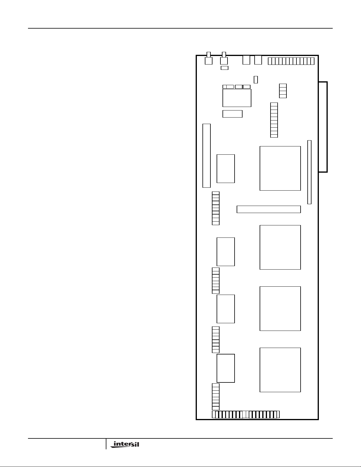
Appendix A - Circuit Board Layout
JP10
JP7JP8
JP11
U10
JP5
J2
U4
J6
JP9
JP6
U9
J4
U3
U2
JP2 JP3 JP4
U1
J3
U8
U7
U6
14
JP1
J1
SERINADE™ is a trademark of Intersil Corporation.
SIGLAB™ a trademark of The Athena Group, Inc.
Page 15

Appendix B - Initial Jumper Settings
HSP50215EVAL
INITIAL JUMPER SETTINGS
LOCATION SETTING
J1 3-4
J1 5-6
J1 7-8
J1 9-10
J1 11-12
J1 13-14
J1 15-16
J1 17-18
J1 23-24
J1 25-26
J1 27-28
J1 29-30
J1 31-32
J1 33-34
J1 35-36
J1 37-38
The J1 jumpers are installed to terminate the Channel 4 cascade
input, which is unused in the standard configuration
JP1 5-6
JP1 9-10
JP1 11-12
JP1 13-14
The JP1 jumpers set the control signals, such as chip enables, output enables,andchipselectcontrols fortheACTELand HSP50215
for Channel 4
JP2 1-2
JP2 5-6
JP2 9-10
JP2 11-12
JP2 13-14
The JP2 jumpers set the control signals, such as chip enables, output enables,andchipselectcontrols fortheACTELand HSP50215
for Channel 3
JP3 3-4
JP3 5-6
JP3 9-10
JP3 11-12
JP3 13-14
The JP3 jumpers set the control signals, such as chip enables, output enables,andchipselectcontrols fortheACTELand HSP50215
for Channel 2
JP4 1-2
JP4 3-4
JP4 5-6
INITIAL JUMPER SETTINGS (CONTINUED)
LOCATION SETTING
JP4 9-10
JP4 11-12
JP4 13-14
The JP4 jumpers set the control signals, such as chip enables, outputenables,and chip select controls forthe ACTEL and HSP50215
for Channel 1
JP5 1-2
JP5 3-4
JP5 7-8
JP5 9-10
The JP5 jumpers set the SYNC controls, bringing SYNCOUT to the
output connector and routing the SYNCOUT of channel 1
HSP50215 to the SYNCIN on all channels (HSP50215’s) on the
board. The remaining jumpers add additional output signal resolution to the output connector, J2.
JP6 9-10
JP6 11-12
JP6 13-14
JP6 15-16
JP6 17-18
JP6 19-20
The JP6 jumpers set the card address to 110000 and connecting
the card decode to the board circuitry.
JP7 2-3
JP7 sets the clocking configuration to be from the on board crystal
oscillator.
JP8 1-2
JP8 3-4
The JP8 jumpers connect the selected clock to the on board clock
drivers and connect one driver output to the output connector, J2.
JP9 1-2
JP9 5-6
The JP9 jumpers set the control to be from the ISAbus rather than
from the parallel port interface
JP10 1-2
The JP10 jumper terminates an external clock input in 50Ω. While
this jumper is set, no external clock is used in the standard configuration (see jumper JP7)
JP11 1-2
The JP11 jumper connects the 12V from the ISAbus interface,
which is regulated down to the -5V required for the -VEEonboard,
to the board -VEE runs.
15
Page 16

HSP50215EVAL
Evaluation Board Layout Showing Jumper Configuration for
ISAbus Configuration.
JP10
JP7JP8
JP11
U10
JP5
J2
U4
J6
JP9
JP6
U9
J4
Evaluation Board Layout Showing Jumper Configuration for
Parallel Bus Configuration.
JP10
JP7JP8
JP11
U10
JP5
J2
U4
J6
JP9
JP6
U9
J4
U3
U2
JP2 JP3 JP4
U1
J3
U8
U7
U6
U3
U2
JP2 JP3 JP4
U1
J3
U8
U7
U6
JP1
J1
JP1
J1
16
Page 17

HSP50215EVAL
Appendix C - Connector Pin Assignments
J1 CONNECTOR PIN ASSIGNMENTS
PIN SIGNAL PIN SIGNAL
1 N/C 21 NC
2 GND 22 GND
3 CAS15 23 CAS7
4 GND 24 GND
5 CAS14 25 CAS6
6 GND 26 GND
7 CAS13 27 CAS5
8 GND 28 GND
9 CAS12 29 CAS4
10 GND 30 GND
11 CAS11 31 CAS3
12 GND 32 GND
13 CAS10 33 CAS2
14 GND 34 GND
15 CAS9 35 CAS1
16 GND 36 GND
17 CAS8 37 CAS0
18 GND 38 GND
19 CONNINCLK 39 CASSYNC2
20 GND 40 GND
J2 CONNECTOR PIN ASSIGNMENTS
PIN SIGNAL PIN SIGNAL
1 N/C 21 NC
2 GND 22 GND
3 OUT4_15 23 OUT4_7
4 GND 24 GND
5 OUT4_14 25 OUT4_6
6 GND 26 GND
7 OUT4_13 27 OUT4_5
8 GND 28 GND
9 OUT4_12 29 OUT4_4
10 GND 30 GND
11 OUT4_11 31 OUT4_3
12 GND 32 GND
13 OUT4_10 33 OUT4_2
14 GND 34 GND
15 OUT4_9 35 OUT4_1
16 GND 36 GND
17 OUT4_8 37 OUT4_0
18 GND 38 GND
19 MASTERCLK 39 OPCASSYNC
20 GND 40 GND
J3 CONNECTOR PIN ASSIGNMENTS
PIN SIGNAL PIN SIGNAL
1 GND 2 GND
3 A3_0 4 OERAM4
5 FIFOTP_4 6 C4_15
7 CEPULLUP_4 8 C4_14
9 SYMBLCLK_4 10 C4_13
11 WR215_4 12 C4_12
13 OE215_4 14 C4_11
15 RESET4 16 C4_10
17 GND 18 GND
19 DU4A9 20 C4_9
21 DU4A8 22 C4_8
23 DU4A7 24 C4_7
25 DU4A6 26 C4_6
27 DU4A5 28 C4_5
29 DU4A4 30 C4_4
31 DU4A3 32 C4_3
33 DU4A2 34 C4_2
35 DU4A1 36 C4_1
37 DU4A0 38 C4_0
39 GND 40 GND
J4 CONNECTOR PIN ASSIGNMENTS
PIN SIGNAL
1 GND
2 A4_16
3 A4_15
4 A4_14
5 A4_13
6 A4_12
7 A4_11
8 A4_10
9 GND
10 A4_9
11 A4_8
12 A4_7
13 A4_6
14 A4_5
15 A4_4
16 A4_3
17 A4_2
18 A4_1
19 A4_0
20 GND
17
Page 18

HSP50215EVAL
J5 CONNECTOR PIN ASSIGNMENTS
PIN SIGNAL
1 ANALOG IF
2 GND
J6 CONNECTOR PIN ASSIGNMENTS
PIN SIGNAL
1 SMACLK
2 GND
J7 CONNECTOR PIN ASSIGNMENTS
PIN SIGNAL
1 -5V
2 GND
J8 CONNECTOR PIN ASSIGNMENTS
PIN SIGNAL
1 SVCC
2 GND
J9 CONNECTOR PIN ASSIGNMENTS
PIN SIGNAL PIN SIGNAL
1 N/C 1 N/C
2 PCD0 2 N/C
3 PCD1 3 PARWR
4 PCD2 4 PARA
5 PCD3 5 GND
6 PCD4 6 GND
7 PCD5 7 GND
8 PCD6 8 GND
9 PCD7 9 GND
10 NC 10 GND
11 STAT 11 GND
12 N/C 12 GND
13 N/C 13 GND
EE
J10 CONNECTOR PIN ASSIGNMENTS
PIN SIGNAL PIN SIGNAL
1 -IOCHK 32 GND
2 D7 33 RESDRV
3 D6 34 +5V
4 D5 35 IRQ9
5 D4 36 -5V
6 D3 37 DREQ2
7 D2 38 -12V
8 D1 39 -0WS
9 D0 40 +12V
10 IOCHRDY 41 GND
11 AEN 42 -SMEMW
12 A19 43 -SMEMR
13 A18 55 -IOW
14 A17 45 -IOR
15 A16 46 -DACK3
16 A15 47 DREQ3
17 A14 48 -DACK1
18 A13 49 DREQ1
19 A12 50 -REFSH
20 A11 51 SYSCLK
21 A10 52 IRQ7
22 A9 53 IRQ6
23 A8 54 IRQ5
24 A7 55 IRQ4
25 A6 56 IRQ3
26 A5 57 -DACK2
27 A4 58 TC
28 A3 59 ALE
29 A2 60 +5V
30 A1 61 14.3MHz
31 A0 62 GND
18
Page 19

HSP50215EVAL
Appendix D - Test Header Pin Assignments
JP1 TEST HEADER PIN ASSIGNMENTS
PIN SIGNAL DESCRIPTION PIN SIGNAL DESCRIPTION
1 GND Ground 2 CSEL0_1 CSEL0_1
3 GND Ground 4 CSEL1_1 CSEL1_1
5 GND Ground 6 CSEL2_1 CSEL2_1
7 GND Ground 8 Unused Unused
9 GND Ground 10 ACTELEN_1 ACTEL ENABLE FOR U6
11 GND Ground 12 OEPULLUP_1 OUTPUT ENABLE PULLUP U1
13 GND Ground 14 CEPULLUP_1 CHIP ENABLE U1 PULLUP_1
15 GND Ground 16 FIFOTP_1 FIFO TEST POINT U1
JP2 TEST HEADER PIN ASSIGNMENTS
PIN SIGNAL DESCRIPTION PIN SIGNAL DESCRIPTION
1 GND Ground 2 CSEL0_2 CSEL0_2
3 GND Ground 4 CSEL1_2 CSEL1_2
5 GND Ground 6 CSEL2_2 CSEL2_2
7 GND Ground 8 Unused Unused
9 GND Ground 10 ACTELEN_2 ACTEL ENABLE FOR U7
11 GND Ground 12 OEPULLUP_2 OUTPUT ENABLE PULLUP U2
13 GND Ground 14 CEPULLUP_2 CHIP ENABLE U2 PULLUP_1
15 GND Ground 16 FIFOTP_2 FIFO TEST POINT U2
JP3 TEST HEADER PIN ASSIGNMENTS
PIN SIGNAL DESCRIPTION PIN SIGNAL DESCRIPTION
1 GND Ground 2 CSEL0_3 CSEL0_3
3 GND Ground 4 CSEL1_3 CSEL1_3
5 GND Ground 6 CSEL2_3 CSEL2_3
7 GND Ground 8 Unused Unused
9 GND Ground 10 ACTELEN_3 ACTEL ENABLE FOR U8
11 GND Ground 12 OEPULLUP_3 OUTPUT ENABLE PULLUP U3
13 GND Ground 14 CEPULLUP_3 CHIP ENABLE U3 PULLUP_1
15 GND Ground 16 FIFOTP_3 FIFO TEST POINT U3
JP4 TEST HEADER PIN ASSIGNMENTS
PIN SIGNAL DESCRIPTION PIN SIGNAL DESCRIPTION
1 GND Ground 2 CSEL0_4 CSEL0_4
3 GND Ground 4 CSEL1_4 CSEL1_4
5 GND Ground 6 CSEL2_4 CSEL2_4
7 GND Ground 8 Unused Unused
9 GND Ground 10 ACTELEN_4 ACTEL ENABLE FOR U9
11 GND Ground 12 OEPULLUP_4 OUTPUT ENABLE PULLUP U4
13 GND Ground 14 CEPULLUP_4 CHIP ENABLE U4 PULLUP_1
15 GND Ground 16 FIFOTP_4 FIFO TEST POINT U4
19
Page 20

HSP50215EVAL
JP5 TEST HEADER PIN ASSIGNMENTS
PIN SIGNAL DESCRIPTION PIN SIGNAL DESCRIPTION
1 OUT4_1 2ND TO LSB OF OUTPUT OF
CHANNEL 1 OUTPUT
3 OUT4_0 LSB OF OUTPUT OF CHANNEL Q
OUTPUT
5 CASSYNC OFF BOARD (J1) SYNC DRIVER
INPUT AND SYNCIN/SYNCOUT
JUMPER POINTS
7 SYNCIN HSP50215 SYNCIN INPUT FOR
CHANNELS 1, 2, 3, AND 4
9 SYNCOUT SYNCOUT OUTPUT FROM CHAN-
NEL1HSP50215 ASSOURCEFOR
SYNC SIGNAL
JP6 TEST HEADER PIN ASSIGNMENTS
PIN SIGNAL DESCRIPTION PIN SIGNAL DESCRIPTION
1 GND CHIPSELECT 2 GROUND CHIPSELECT HARDWIRE ZERO
3 GND UNUSED 4 GROUND UNUSED
5 GND PULLUP AND ISA CARD
ADDRESS DECODE BIT 9 (MSB)
7 GND PULLUP AND ISA CARD
ADDRESS DECODE BIT 8
9 GND PULLUP AND ISA CARD
ADDRESS DECODE BIT 7
11 GND PULLUP AND ISA CARD
ADDRESS DECODE BIT 6
13 GND PULLUP AND ISA CARD
ADDRESSDECODE BIT 5
15 GND PULLUP AND ISA CARD
ADDRESS DECODE BIT 4
17 GND PULLUP AND ISA CARD
ADDRESS DECODE ENABLE BIT
19 GND ISA CARD DECODE 20 U23- 4, 5, 9 AND 12 ENABLE FOR ISABUS READ,
2 OPOUT1 OUTPUT LSB+1
4 OPOUT0 OUTPUT LSB
6 OPCASSYNC CASCADE SYNC OUTPUT ON
OUTPUT CONNECTOR J2
8 U11-11 AND JP5-8,10OFF BOARD (J1) SYNC DRIVER
INPUT AND SYNCIN/SYNCOUT
JUMPER POINTS
10 U11-2, 4, 6, 8 OFF BOARD (J1) SYNC DRIVER
INPUT AND SYNCIN/SYNCOUT
JUMPER POINTS
6 GROUND CARD ADDRESS HARDWIRE
ZERO
8 GROUND CARD ADDRESS HARDWIRE
ZERO
10 GROUND CARD ADDRESS HARDWIRE
ZERO
12 GROUND CARD ADDRESS HARDWIRE
ZERO
14 GROUND CARD ADDRESS HARDWIRE
ZERO
16 GROUND CARD ADDRESS HARDWIRE
ZERO
18 GROUND CARD ADDRESS HARDWIRE
ZERO
WRITE AND DATA BUS
JP7 TEST HEADER PIN ASSIGNMENTS
PIN SIGNAL DESCRIPTION
1 SMACLK J3 SMA CLOCK INPUT
2 OSCLCK CLOCK SELECTION, OUTPUT
3 CRYSTALCLK CRYSTAL CLOCK OUTPUT
20
JP8 TEST HEADER PIN ASSIGNMENTS
PIN SIGNAL DESCRIPTION
1 OSCLCK SELECTED CLOCK SOURCE
2 DU3A9 CLOCK DRIVER INPUT
3 J2-17 OUTPUT CONNECTOR PIN 17
4 MASTERCLK MASTER CLOCK OUTPUT
Page 21

HSP50215EVAL
JP9 TEST HEADER PIN ASSIGNMENTS
PIN SIGNAL DESCRIPTION PIN SIGNAL DESCRIPTION
1 GND ISA INPUT ADDRESS 2 A ADDRESS
3 PARA PARALLEL INPUT ADDRESS 4 A ADDRESS
5 LIOW ISA INPUT WRITE 6 WR WRITE
7 PARWR PARALLEL INPUT WRITE 8 WR WRITE
JP10 TEST HEADER PIN ASSIGNMENTS
PIN SIGNAL DESCRIPTION
1 SMACLK J3 SMA CLOCK INPUT
250Ω - GND TERMINATION RESISTOR
JP11 TEST HEADER PIN ASSIGNMENTS
PIN SIGNAL DESCRIPTION PIN SIGNAL DESCRIPTION
1 REGULATED -5.2V REGULATED -5.2V SOURCED
FROM ISA BUS INTERFACE
2 CARD -V
EE
-V
EE
21
Page 22

HSP50215EVAL
Appendix E - Detailed Schematics
22
Page 23

HSP50215EVAL
(Continued)
Appendix E - Detailed Schematics
23
Page 24

HSP50215EVAL
(Continued)
Appendix E - Detailed Schematics
24
Page 25

HSP50215EVAL
(Continued)
Appendix E - Detailed Schematics
25
Page 26

HSP50215EVAL
(Continued)
Appendix E - Detailed Schematics
26
Page 27

HSP50215EVAL
(Continued)
Appendix E - Detailed Schematics
27
Page 28

HSP50215EVAL
(Continued)
Appendix E - Detailed Schematics
28
Page 29

HSP50215EVAL
(Continued)
Appendix E - Detailed Schematics
29
Page 30

HSP50215EVAL
(Continued)
Appendix E - Detailed Schematics
30
Page 31

HSP50215EVAL
(Continued)
Appendix E - Detailed Schematics
31
Page 32

HSP50215EVAL
(Continued)
Appendix E - Detailed Schematics
32
Page 33

HSP50215EVAL
(Continued)
Appendix E - Detailed Schematics
33
Page 34

HSP50215EVAL
Appendix F - Parts List
INTERSIL CORPORATION HSP50215EVAL REV B REV. B 3/23/98
QTY
LINE
ITEM
1 4 U1-U4 DIGITAL UPCONVERTER 100 MQFP Intersil HSP50215VC
2 8 U13 - U20 1 MBIT STATIC RAM 32 SOJ IDT IDT71024S15TY
3 4 U6 - U9 FPGA 84 PLCC ACTEL A1225XL-PL84C
4 4 REF U6-U9 Label to read on FPGA:
5 1 U5 14-BIT D/A 28 SOIC Intersil HI5741BIB
6 3 JP1 - JP3 HEADER 2 x 8 2 x 8 QPL/SULLINS PTC8DAAN
6A 1 J9 HEADER 2 x 13, SHROUDED 2 x 13 CIRCUIT ASSEMBLY
7 2 JP4, 6 HEADER 2 x 10 2 x 10 QPL/SULLINS PTC10DAAN
8 1 JP9 HEADER 2 x 4 2 x 4 QPL/SULLINS PTC4DAAN
9 2 JP10, 11 HEADER 1 x 2 1 x 2 QPL/SULLINS PTC2SAAN
10 1 JP7 HEADER 1 x 3 1 x 3 QPL/SULLINS PTC35SAAN
11 1 JP8 HEADER 1 x 4 1 x 4 QPL/SULLINS PTC4SAAN
12 1 J4 HEADER 1 x 20 1 x 20 QPL/SULLINS PTC20SAAN
13 1 JP5 HEADER 2 x 5 2 x 5 QPL/SULLINS PTC5DAAN
14 3 J1, J2, J3 HEADER 2 X 20 2 x 20 QPL/SULLINS PTC20DAAN
15 10 RZ - RZ10 22K RPACK TO PIN SM SIP 10 PIN SIP PANASONIC EXB-H110223J
16 1 XU10 14 PIN SOCKET SOCKET QPL/AUGAT 814-AG11D
17 1 U10 XTAL OSC 50MHz 14 DIP QPL/CTS MX-45T-50,000
18 1 U21 IC 20 SOIC NATIONAL 74ACT520SC
19 1 U23 IC 14 SOIC Intersil 74ACT32M
20 1 U24 IC 20 SOIC Intersil 74ACT245M
21 2 U11, U22 IC 20 SOIC Intersil 74ACT244M
22 1 U12 VOLT, REGULATOR -5.2V TO220 NATIONAL SEMI LM29905-5.2
23 1 C6 CAPACITOR, SM 0.1µF 1210 QPL/PANASONIC ECH-U1C104JB5
24 8 C5, 61 - 66, 69 CAPACITOR, 10µF RADIAL QPL/MALLORY TDC106M025NSF
25 58 C1, 2, 7-60, 67, 68 CAPACITOR, SM, 0.01µF 1206 QPL/PANASONIC ECH-U1C103JB5
26 2 R6, 7 RESISTOR, SM, 62Ω 1210 QPL/PANASONIC ERJ-14YJ62
27 1 R8 RESISTOR, SM 910Ω 1210 QPL/PANASONIC ERJ-14YJ910
28 6 R1 - 5, 11 RESISTOR, SM 20Ω 1210 QPL/PANASONIC ERJ-14YJ20
29 2 RA1, R31 RESISTOR, SM 50Ω 1210 QPL/PANASONIC ERJ-14YJ50
30 2 J5, 6 ANGLE PCB MOUNT AMPHONEL/DIGIKEY ARF1232-ND
31 50 SHORTING JUMPERS QPL/SULLINS STC02SYAN
32 2 J7, 8 DJ0058 POWER PLUG QPL/LZR RL30B
33 2 CABLE, DC10B QPL/LZR DC10B
34 15 R15-28, 30 RESISTOR, SM, 200Ω 1206 QPL/PANASONIC ERJ-8GEYJ200
35 1 RIBBON CABLE W/CONN DIGLKEY M1AXA-2636R-ND
36 1 CONNECTOR, 25D, IDC QPL/3M 8225-6000
37 C3, C4, C100, R9,
38 1 TBD BOLT
39 1 TBD WASHER
41 1 PWB
42 1 DISKETTE
43 1 MANUAL
40 1 STATIC BAG
44 1 BOX
PER
PCB
1 TBD NUT
REFERENCE
DESIGNATOR DESCRIPTION PKG MANUFACTURER
R10, R12 - 14, R29,
R100
HSP50215
FPGA REV A
OPTIONAL PARTS FOR
PARALLEL CONTROL
MANUFACTURER’S
CA-28HL-1C
CORP
PART #
34
Page 35

HSP50215EVAL
Appendix G - Descriptive File List
PC PROGRAM
FILE DESCRIPTION
HSP50215.EXE HSP50215EVAL CONTROL
SOFTWARE PROGRAM
MISCELLANEOUS
FILE DESCRIPTION
EXxx
name
.CFG EXAMPLE CONFIGURATION FILES
filename
.IMP REFERENCE EXAMPLE FILTER FILES
filename
.IMP REFERENCE EXAMPLE STIMULUS
FILES
Example Configuration Files
The example configuration files are located in the
EXAMPLES subdirectory. Load the desired example
configuration file using menu item 5 in the main menu. The
naming convention for the example configuration files is:.
EX
xx
NAME
FILE NAME
EXAMPLE NUMBER
EXAMPLE CONFIGURATION FILE
File Name: EX02GMSK
Description:
This is an example of GMSK using the FM with pre-filter.The
BT product is 0.3 (GSM). The input sample rate is
270.833kHz. The data is a 511 sample PN. The PN codes
for channels 2 and 4 are pre-coded to give the proper data
when demodulated as OQPSK at 135.417 kbaud. When
using this configuration with bursts for GSM, it does not
support guard times of less than full data bit periods due to
that input sample rate. To generate guard times with quarter
bit resolution, the input sample rate must be increased to
4x270833. The channel spacing is 800kHz with one
unoccupied channel. With the supplied 50MHz oscillator, the
maximum input sample rate supported by this configuration
is 625,000Hz.
EX02GMSK EXAMPLE CONFIGURATION FILE
Channel 1 Channel 2 Channel 3 Channel4
Filter file: GS5T16X GS5T16X GS5T16X GS5T16X
IP / DS: 16 / 5 16 / 5 16 / 5 16 / 5
Center
Frequency:
Input
Sample
Rate:
Stimulus
File:
3200000 4000000 4800000 6400000
270833.333 270833.333 270833.333 270833.333
GMSKPN GMSKPN-PCGMSKPN GMSKPN-
PC
File Name: EX01QPSK
Description:
This example illustrates high dynamic range QPSK
modulation. It is similar to IS136, but with a continuous 511
sample long PN sequence and QPSK modulation instead of
Pi/4DQPSK modulated in bursts. The filter is a square root of
raised cosine with a = 0.35. The channel spacing is 120kHz
with one unoccupied channel. With the supplied 50MHz
oscillator, the maximum input sample rate supported by this
configuration is 195,312.5Hz.
EX01QPSK EXAMPLE CONFIGURATION FILE
Channel 1 Channel 2 Channel 3 Channel4
Filter file: IS136B IS136B IS136B IS136B
IP / DS: 16 / 16 16 / 16 16 / 16 16 / 16
Center
Frequency:
Input
Sample
Rate:
Stimulus
File:
4000000 4120000 4240000 4480000
24300 24300 24300 24300
QPSKPN QPSKPN QPSKPN QPSKPN
File Name: EX03QPSK
Description:
This is a lower dynamic range QPSK example. This filter is a
slightly modified version of the IS95 coefficient set. The
stimulus is a 511 PN sequence on I and Q. The channel
spacing is 1.25 times the symbol rate. With the supplied
50MHz oscillator, the maximum input sample rate supported
by this configuration is 1.041667MHz.
EX03QPSK EXAMPLE CONFIGURATION FILE
Channel 1 Channel 2 Channel 3 Channel4
Filter file: IS95MOD IS95MOD IS95MOD IS95MOD
IP / DS: 4 / 12 4 / 12 4 / 12 4 / 12
Center
Frequency:
Input
Sample
Rate:
Stimulus
File:
4000000 4768000 5536000 6304000
614400 614400 614400 614400
QPSKPN QPSKPN QPSKPN QPSKPN
35
Page 36

HSP50215EVAL
File Name: EX04QAM
Description:
This file demonstrates 16QAM modulation. The filter is a
square root of raised cosine response (a = 0.2). The
stimulus file is 511 PN codes on each data bit. The channel
spacing is 1.5 times the symbol rate. With the supplied
50MHz oscillator, the maximum input sample rate supported
by this configuration is 1.041667MHz.
EX04QAM EXAMPLE CONFIGURATION FILE
Channel 1 Channel 2 Channel 3 Channel4
Filter file: RRC2A4X RRC2A4X RRC2A4X RRC2A4X
IP / DS: 4 / 12 4 / 12 4 / 12 4 / 12
Center Fre-
quency:
Input
Sample
Rate:
Stimulus
File:
4000000 4768000 5536000 6304000
512000 512000 512000 512000
16QAMPN 16QAMPN 16QAMPN 16QAMPN
File Name: EX05QPSK
Description:
This is an example of a higher rate QPSK modulator for
applications such as Satellite Communication. The filter is a
square root of raised cosine response α = 0.35. The filter
impulse response is short to support higher data rates. For
lower data rates, the filter in EX01QPSK is recommended.
The channel spacing is 1.4 times the symbol rate. With the
50MHz oscillator, the maximum input sample rate for this
configuration is 1.5625 MSPS.
EX05QPSK EXAMPLE CONFIGURATION FILE
Channel 1 Channel 2 Channel 3 Channel4
Filter file: RRC35A4X RRC35A4X RRC35A4X RRC35A4
X:
IP / DS 4 / 8 4 / 8 4 / 8 4 / 8
Center Fre-
quency:
Input
Sample
Rate:
Stimulus
File:
4000000 4360000 4720000 5080000
256000 256000 256000 256000
QPSKPN QPSKPN QPSKPN QPSKPN
File Name: EX06QPSK
Description:
This example is similar to EX01QPSK, but used for co-
channel and adjacent channel testing. The desired signal is
in channel 2. Channels 1 and 3 are at 1.4 times the symbol
rate offsets and +10dB higher than the desired signal.
Channel 4 is in the same channel as the desired signal and
10dB lower. The data rates are offset slightly to randomize
the phasing of the channels.
EX06QPSK EXAMPLE CONFIGURATION FILE
Channel 1 Channel 2 Channel 3 Channel4
Filter file: IS136B IS136B IS136B IS136B
IP / DS: 16 / 16 16 / 16 16 / 16 16 / 16
Center
Frequency:
Input
Sample
Rate:
Stimulus
File:
4000000 4034000 4068000 4034000
24300.2 24300 24300.3 24300.1
QPSKPN QPSKPN QPSKPN QPSKPN
File Name: EX07FM
Description:
The is an example of analog FM modulation with post-
modulation filtering. The filter is a fairly tight low pass design.
This is probably tighter than would be necessary or desired
for AMPS modulation. The tight filtering introduces some
harmonic distortion in the recovered baseband signal. The
stimulus files are all 1kHz sine waves at 60ksps with 8, 7, 6,
and 8kHz deviations for channels 1-4, respectively. The
channel spacing is 120kHz with one channel unoccupied.
With the 50MHz oscillator, the maximum input sample rate
would be 390.625kHz. At this rate, the modulation would be
6.5kHz sine waves.
EX07FM EXAMPLE CONFIGURATION FILE
Channel 1 Channel 2 Channel 3 Channel4
Filter file: AMPS2 AMPS2 AMPS2 AMPS2
IP / DS: 8 / 16 8 / 16 8 / 16 8 / 16
Center
Frequency:
Input
Sample
Rate:
Stimulus
File:
4000000 4120000 4240000 4480000
60000 60000 60000 60000
FM1K8K FM1K7K FM1K6K FM1K8K
36
Page 37

HSP50215EVAL
File Name: EX08FSK
Description:
This file is similar to EX07FM but with different stimulus
patterns. Channel 1 is modulated with a 10 kbps,
Manchester encoded, length 511, PN sequence at a
deviation of ±8kHz. Channel 2 through 4 are 1kHz sine
waves with deviations of ±3, 4, and 5kHz, respectively.
EX08FSK EXAMPLE CONFIGURATION FILE
Channel 1 Channel 2 Channel 3 Channel4
Filter file: AMPS2 AMPS2 AMPS2 AMPS2
IP / DS: 8 / 16 8 / 16 8 / 16 8 / 16
Center
Frequency:
Input Sam-
ple Rate:
Stimulus
File:
4000000 4120000 4240000 4480000
60000 60000 60000 60000
FSKPN FM1K3K FM1K4K FM1K5K
File Name: EX09TONE
Description:
This is an example of multi-tone modulation. Each channel
modulates 7 tones onto its carrier (8 slots - 1 unoccupied).
The tone spacing is 16kHz. With all channels enabled, there
is a total of 28 tones. The filter file is slightly wider than the
AMPS2 file to pass the tones without attenuating the outer
tones. The tones in each channel are phase aligned at zero
phase. Due to the pipeline delays in the cascade data path,
the four channels will not be phase aligned.
EX09TONE EXAMPLE CONFIGURATION FILE
Channel 1 Channel 2 Channel 3 Channel4
Filter file: GP2 GP2 GP2 GP2
IP / DS: 16 / 16 16 / 16 16 / 16 16 / 16
Center
Frequency:
Input Sam-
ple Rate:
Stimulus
File:
4000000 4128000 4256000 4384000
192000 192000 192000 192000
MTONE1 MTONE1 MTONE1 MTONE1
File Name: EXxxNAME
Description:
This is a blank table for your own example configuration files.
EX_______ EXAMPLE CONFIGURATION FILE
Channel 1 Channel 2 Channel 3 Channel4
Filter file:
IP / DS:
Center
Frequency:
Input Sam-
ple Rate:
Stimulus
File:
Example Filter Files
.IMP File Format
The .IMP file is an ASCII text file containing filter coefficients
or stimulus vectors. An example of the .IMP file format is
shown below. This format matches the format used by
SIGLAB, a DSP simulation program by the Athena Group
Inc. of Gainesville, Florida. In SIGLAB, the first four lines are
used for comments, the fifth line for x-axis labels, the sixth
line for y-axis labels, and the seventh line contains: t c r,
where t is “r” for real data and “c” for complex data, c is the
number of columns, and r is the number of rows. In the
evaluation board software, the first seven lines are ignored
by the program, so all seven lines may be used for
comments. The program requires complex sample pairs
even if a real signal is modulated (such as in FM). The first
sample of the pair is the I data and the second is the Q data.
The values of the samples can range from -1.0 to +1.0.
When the program reads in the data, it multiplies it by 2
and rounds to 16 bits. If the scaled data exceeds the range 32767 to +32767, the program saturates it to those values.
An example of the .IMP file format is shown below:
FILTER FOR IS-136 WAVEFORMS
ROOT RAISED COSINE
ALPHA = 0.35, 256 TAPS @ 16X BAUD
DC GAIN = 0.658 (-3.64dBFS)
PEAK COEF = 0.721
MAXIMUM OUTPUT = 1.054 (+0.4dB)
C 2 256
0.000213623 0.000213623
0.000671387 0.000671387
0.000640869 0.000640869
6.10352E-05 6.10352E-05
-0.000640869 -0.000640869
-0.001312256 -0.001312256
-0.001922607 -0.001922607
-0.002410889 -0.002410889
-0.002746582 -0.002746582
-0.002929688 -0.002929688
-0.00289917 -0.00289917
-0.002685547 -0.002685547
When loading filter coefficients, the program will report an
error if the number of samples exceeds the number allowed
for the selected IP value.
15
37
Page 38

HSP50215EVAL
File name: IS136B.IMP
PARAMETER VALUE
TAPS 256@16XF
IP / DS: 16 / 16
3dB BW 0.5 x F
DC Gain 0.658 (-3.64dBFS)
Peak Coef Value 0.72114562
Maximum Output 1.054336176 (+0.4dB)
NBW: 1.004 x F
Description:
Square root of raised cosine filter (alpha = 0.35) for North
American TDMA cellular type signals
Frequency Response
(DC to FOUT/2 of the Shaping FIR Filter)
SAMP
SAMP
SAMP
(double sided)
File name: RRC2A4X.IMP
PARAMETER VALUE
Taps: 48 @4x F
IP / DS: 4 / 12
3dB BW 0.5 x F
DC Gain 0.595 (-4.5dB)
Peak Coef Values 0.610
Maximum Output 1.094 (+0.78dB)
NBW: 0.996 x F
Description:
Square root of raised cosine filter with sharp transition band
(alpha = 0.2) for QAM type signals.
Frequency Response.
(DC to Fout/2 of the Shaping FIR Filter)
.
SAMP
SAMP
SAMP
(double sided)
FIGURE 9. IS136B.IMP FREQUENCY RESPONSE
FIGURE 10. RRC2A4X.IMP FREQUENCY RESPONSE
38
Page 39

HSP50215EVAL
File name: GS5T16X.IMP
PARAMETER VALUE
Taps: 80 @16xF
IP / DS: 16 / 5
3dB BW ~0.25 x F
DC Gain 1.0000 (0dB)
Peak Coef Value 0.7416
Maximum Output 1.0000 (+0dB)
NBW: 0.53 x F
Description:
Gaussian filter for GSM (GMSK). BT = 0.3 Filter must be
stimulated with ±0.03125 for proper spectrum
Frequency Response (into FM Modulator)
(DC to F
/2 of the Pre-modulation Shaping FIR Filter)
OUT
SAMP
SAMP
(double sided)
SAMP
File name: S95MOD.IMP
PARAMETER VALUE
Taps: 48 @xF
IP / DS: 4 / 12
3dB BW Approx 0.5 x F
DC Gain 0.543 (-5.3dB)
Peak Coef Value 0.498
Maximum Output 1.05 (+0.42dB)
NBW: 1.012xF
Description:
Filter coefficients from IS95 Specification, rounded and then
scaled to minimize AM.
Frequency Response
(DC to F
/2 of the Shaping FIR Filter)
OUT
SAMP
SAMP
(double sided)
SAMP
FIGURE 11. GS5T16X.IMP FREQUENCY RESPONSE
FIGURE 12. S95MOD.IMP FREQUENCY RESPONSE
39
Page 40

HSP50215EVAL
File name: AMPS2.IMP
PARAMETER VALUE
Taps: 128 @8xF
IP / DS: 8 / 16
3dB BW ~0.225 x F
(13.5kHz @ F
DC Gain 0.500 (-6.02dB)
Peak Coef Value 0.244
Maximum Output 0.728 (-2.76dB)
NBW: 0.456 x F
Description:
Post modulation filter for AMPS type FM signals. Signals.
With F
= 60kHz, response is >36dB down at 20kHz
SAMP
and >70dB down for frequencies > 23kHz. Passband ripple
is 0.5dB peak to peak.
Frequency Response
(DC to F
/2 of the Shaping FIR Filter
OUT
SAMP
SAMP
SAMP
(double sided)
SAMP
= 60kHz)
File name: RRC35A4X.IMP
PARAMETER VALUE
Taps: 32 @4xF
IP / DS: 4 / 8
3dB BW 0.5 x F
DC Gain 0.50 (-6dB)
Peak Coef Value 0.610
Maximum Output 0.757 (-2.41dB)
NBW: 0.989 x F
Description:
Square root of raised cosine filter for higher rate (to ~1.5
Mbaud) Satcom type signals.
Frequency Response
(DC to F
/2 of the Shaping FIR Filter)
OUT
SAMP
SAMP
SAMP
(double sided)
FIGURE 13. AMPS2.IMP FREQUENCY RESPONSE
40
FIGURE 14. RRC35A4X.IMP FREQUENCY RESPONSE
Page 41

HSP50215EVAL
File name: GP1.IMP
PARAMETER VALUE
Taps: 256 @16xF
IP / DS: 16 / 16
3dB BW ~0.3 x F
DC Gain 0.518 (-5.7dB)
Peak Coef Value 0.345
Maximum Output 0.835 (-1.57dB)
NBW: 0.606 x F
Description:
High dynamic range filter for general purpose interpolation.
Passband ripple is 0.3dB peak to peak.
Frequency Response
(DC to F
/2 of the Shaping FIR Filter)
OUT
SAMP
SAMP
SAMP
(double sided)
File name: GP2.IMP
PARAMETER VALUE
Taps: 256 @16xF
IP / DS: 16 / 16
3dB BW ~0.38 x F
DC Gain 0.51 (-5.7dB)
Peak Coef Value 0.433
Maximum Output 0.835 (-1.57dB)
NBW: 0.77 x F
Description:
High dynamic range filter for general purpose interpolation.
Passband ripple is 0.1dB peak to peak.
Frequency Response
(DC to F
/2 of the Shaping FIR Filter)
OUT
SAMP
SAMP
(double sided)
SAMP
FIGURE 15. GP1.IMP FREQUENCY RESPONSE
FIGURE 16. GP2.IMP FREQUENCY RESPONSE
File name: BYPASS.IMP
PARAMETER VALUE
Taps: 16 @4xF
IP / DS: 4 / 4
3dB BW N/A
DC Gain 32767/32768 (-0.00027dBFS)
Peak Coef Value 32767/32768
Maximum Output 32767/32768 (-0.00027dBFS)
NBW: N/A
Description:
Shaping filter bypass mode. Input samples are scaled by
32767/32768 and repeated for one input sample time (four
shaping filter output cycles.) Use for evaluating carrier NCO
purity as AM from the filtering is produced.
Frequency Response: Sin(X)/X with nulls aligned with the
interpolation filter nulls.
SAMP
41
Page 42

HSP50215EVAL
Example Stimulus Files
When the program loads stimulus vectors, it first counts the
sample pairs to calculate the first RAM address for loading. It
then reads in the data and writes it to the pattern RAM. The
maximum number of sample pairs is 65536 (the RAM holds
up to 128kwords).
File Name: BPSKPN.IMP
# Samples: 511
Description: Stimulus file for BPSK modulation. PN
sequence. Same data on I and Q.
Vector Length: 1.0. (0 dBFS); 0.7071 on I and Q
File Name: QPSKPN.IMP
# Samples: 511
Description: Stimulus file for QPSK modulation. PN
sequence. Same sequence on I and Q, offset by 64
samples.
Vector Length: 1.0 (0 dBFS); 0.7071 on I and Q.
File Name: 16QAMPN.IMP
# Samples: 511
Description: Stimulus file for 16 QAM modulation. Summed
PN sequences. I and Q vectors constructed by the Equation:
0.5*PN1 + 0.25*PN2, where PN1 and PN2 can take the
values ±1. Same PN sequence is used for PN1, PN2 for I
and Q with offsets of 0, 64, 25, and 80.
Vector Length: 0.78995 RMS (-2.05 dBFS); 1.061 Max (+0.5
dBFS); ±0.25, 0.75 on I and Q.
File Name: GMSKPN.IMP
# Samples: 511
Description: Stimulus file for GMSK (GSM type, BT = 0.3).
PN sequence on I channel only (Q channel is zeroed.
File Name: FM1K8K.IMP
# Samples: 60
Description: Stimulus file for FM modulation (FM with post-
modulation filtering, AMPS type). At 60 ksps input, the
modulation is a 1kHz sine wave with a peak deviation of
8kHz.
Q samples are zeroed.
Vector Length: Peak amplitude = 8/30 = 0.2667 (-11.48
dBFS)
File Name: FM1K7K.IMP
# Samples: 60
Description: Stimulus file for FM modulation (FM with post-
modulation filtering, AMPS type). At 60 ksps input, the
modulation is a 1kHz sine wave with a peak deviation of
7kHz. Q samples are zeroed.
Vector Length: Peak amplitude = 8/30 = 0.2333 (-12.64
dBFS)
File Name: FM1K6K.IMP
# Samples: 60
Description: Stimulus file for FM modulation (FM with post-
modulation filtering, AMPS type). At 60 ksps input, the
modulation is a 1kHz sine wave with a peak deviation of
6kHz. Q samples are zeroed.
Vector Length: Peak amplitude = 8/30 = 0.2 (-13.98 dBFS)
File Name: IMP
# Samples:
Description:
Vector Length: (dBFS); on I and Q.
Vector Length: 1/32 (-30.1 dBFS); ±0.03125 on I, 0 on Q.
File Name: GMSKPNPC.IMP
# Samples: 1022
Description: Stimulus file for GMSK (GSM type, BT = 0.3).
511 PN sequence on I channel only repeated twice and
precoded to output the PN code when modulated as shaped
FM and demodulated as OQPSK.
Vector Length: 1/32 (-30.1 dBFS); ±0.03125 on I, 0 on Q.
42
Page 43

HSP50215EVAL
Appendix H - Detailed Menu Item Descriptions
Board, Interface Menu (Board Configuration)
ITEM 1: INTERFACE:
(0; 1)
Parallel = 0; ISA = 1
Enter New Value [
ITEM 2: LPT NUMBER:
(Enter New Value [
ITEM 3: CHANNEL 1 FPGA ADDRESS: [
VALUE
(0 to 7)
Enter New Value [
ITEM 4: CHANNEL 2 FPGA ADDRESS: [
VALUE
(0 to 7)
Enter New Value [
ITEM 5: CHANNEL 3 FPGA ADDRESS: [
VALUE
(0 to 7)
Enter New Value [
ITEM 6: CHANNEL 4 FPGA ADDRESS: [
VALUE
(0 to 7)
Enter New Value [
]:
]:
]:
]:
CURRENT VALUE
Current Value
CURRENT VALUE
Current Value
Current Value
Current Value
Current Value
Current Value
]:
]:
CURRENT
]:
CURRENT
]:
CURRENT
]:
CURRENT
]:
ITEM 3: MODULATION TYPE
(0 = QASK; 1 = FM w/Postfilter; 2 = FMw/ Prefilter)
Enter New Value [
This field identifies the modulation type as QASK, FM or
prefiltered FM. When implementing PSK or QAM waveforms,
select 0 and identify a stimulus file that matches the desired
modulation format. Some modulation formats are determined
by an input stimulus file and a particular filter coefficient file.
ITEM 4: COEFFICIENT FILE
Current File Prefix:
Enter File Prefix: (.imp extension assumed)
This field identifies the filter coefficient file to be used in the
shaping filter of the channel selected. See Appendix G Descriptive File List for details on the format of this file type.
ITEM 5: INTERPOLATION (IP)
Interpolation Phases: [
(0 = 4 phases, 1 = 8 phases, 2 = 16 phases)
Enter New Value [
This field identifies the number of interpolation phases in the
filtering.
ITEM 6: IMPULSE RESPONSE LENGTH
Current Value: [
Range is 4 - 16
Current Value
Current # Phases
Current Value
Current IRL
]:
]
]:
]
ITEM 7: OSCILLATOR FREQUENCY
(1,000Hz to 52,000,000Hz)
Current Value:
Enter New Value [
Current Value
]:
MODULATOR CHANNEL 1 (OR 2-4)
CONFIGURATION MENU
ITEM 1: CARRIER CENTER FREQUENCY
Range is -52,000,000Hz to 52,000,000Hz
Current Value:
Enter New Value [
ITEM 2: INPUT SAMPLE RATE
Range is 0.01 to 3.25e6
Current Value:
Enter New Value [
This field identifies the sample rate of the stimulus file to be
used as input data. Set this value at the desired symbol rate,
noting that AWGN stimulus files should be set at least 10x
the associated data channel symbol rate, or the IF
bandwidth. Neither should be set at an even multiple of the
symbol rate.
Current Value
Current Value
Current Value
Current Value
]:
]:
Enter New Value [
This field identifies the number of data samples in the
shaping filter of the identified channel.
ITEM 7: STIMULUS FILE
Current File Prefix:[
Enter File Prefix: (.imp extension assumed)
This field is used for identifying the stimulus file that contains
the I and Q data for the identified modulator channel. See
Appendix G - Descriptive File List for details on the format of
this file type. Include in this field, the path to the file, relative
to the directory that the HSP50215.exe file is located.
Stimulus files send data to both the I and Q FIFO’s in the
HSP50215. Fixed levels ( A) are used for BPSK and QPSK.
Multiple levels are required for higher order PSK and QAM
modulation formats. The stimulus file bpskpn writes the
following values to the (I,Q) FIFO’s: (-0.707, -0.707), (0.707,
0.707), yielding a vector magnitude of 1.
Note: If you have not properly identified the stimulus file or the path to
that file, then the program will not download when you command the
software to configure the board, and will return you to the DOS prompt
at which point you will need to restart the control software and start
from scratch on the configuration.
Current Value
]:
Current Filename
]
43
Page 44

HSP50215EVAL
# DATA SAMPLES
Current Value: [
Current # Data Samples
]
Range is 1-65536
Enter New Value [
Current Value
]:
This field is used to identify the number of data samples to
be retrieved from the Stimulus file listed in item 7. If a CW
signal is desired, identify bpskpn as the Stimulus file and
select the number of data samples to be 1. If a test pattern is
desired, select the number of data samples equal to the
length of the test pattern desired, and edit a stimulus file to
contain the desired data bits, starting at location 0. When
using one of the AWGN stimulus files, identifying a large
number of data samples is desirable. Use of standard PN
leggins such as 2
7
-1, 29-1, 215-1 will allow a commercial Bit
Error Rate Tester to be used on the receive path equipment.
ITEM 9: OUTPUT ATTENUATION
Range is 0.00 to 48.0 (more than 48 turns the output off)
Current Value: [
Current Output Attenuation Setting
Enter New Value [
Current Value
]:
]
This field will control the GAIN_CONTROL for the
Programmable Upconverter for the channel identified. Enter
the desired attenuation in dB.
ITEM 10: OUTPUT
Current Value: [
Current Output Enable Setting
]
0 = Disabled
1 = Enabled
Enter New Value [
Current Value
]:
The field sets the output enable condition for the channel
identified.
ITEM 11: CASCADE INPUT
Current Value: [
Current Cascade Input Setting
]
0 = Disabled
1 = Enabled
Enter New Value[
Current Value
]:
This field is used to set the enable state of the cascade input
to the channel identified. Remember that channel 4
cascades into channel 3, and likewise channel 3 into
channel 2 and channel 2 into channel 1.
ITEM 12: SYNC
Current Value: [
Current Sync Setting
]
0 = External
1 = Internal
ITEM 13: SYNC POLARITY
Current Value: [
Current Sync Polarity Setting
]
0 = H ⇒ L
1 = L ⇒ H
Enter New Value[
Current Value
]:
This field is used to set the Sync polarity for the channel
identified.
ITEM 14: FIFO DEPTH
Current Value: [
Current FIFO Depth Setting
]
Range is 1-7
Enter New Value[
Current Value
]:
This field is used to set the I and Q FIFO depth on the
channel identified.
ITEM 15: OUTPUT FORMAT
Current Value: [
Current Output Format Setting
]
0 = Offset Binary
1 = Two’s Complement
Enter New Value[
Current Value
]:
This field sets the output format of the channel identified.
ITEM 16: TEST REGISTER
Current Value: [
Enter New Value[
Current Test Register Setting
Current Value
]:
]
This field sets the value of Control Register 23 of the
channel identified. Standard configurations set this field to 0.
LOAD CONFIGURATION FILE
Current File is: [
Current Configuration File Name
]
Enter New Prefix:
This field is used to identify a configuration file to be loaded
for use or editing. See Appendix G - Descriptive File List for
file format.
SAVE CONFIGURATION FILE
Current File is: [
Current Configuration File Name
]
Enter New Prefix:
This field is used to save the current configuration as a file.
Warning: If a configuration change has been made, and a new file name
is not entered, the changed configuration will be written over the original file. This may destroy example files that are provided with the control
software.
Enter New Value[
Current Value
]:
This field sets the state of the sync control for the identified
channel.
44
Page 45

HSP50215EVAL
BOARD INTERFACE MENU (CONFIGURE BOARD
ITEM 1: CONFIGURE CHANNEL 1
This command downloads the configuration files necessary
to configure only modulator channel #1. All other modulator
channels remain unchanged from the current settings.
ITEM 2: CONFIGURE CHANNEL 2
This command downloads the configuration files necessary
to configure only modulator channel #2. All other modulator
channels remain unchanged from the current settings.
ITEM 3: CONFIGURE CHANNEL 3
This command downloads the configuration files necessary
to configure only modulator channel #3. All other modulator
channels remain unchanged from the current settings.
ITEM 4: CONFIGURE CHANNEL 4
This command downloads the configuration files necessary
to configure only modulator channel #4. All other modulator
channels remain unchanged from the current settings.
ITEM 5: CONFIGURE ALL CHANNELS
This command downloads the configuration files necessary
to configure all four modulator channels.
TEST MENU
ITEM 1: RESET BOARD
This item resets the HSP50215 Digital UpConverters and puts
the ACTEL PLD’ s in their initial state on all four channels.
ITEM 2: WRITE TO LOCATION WHILE RESET
This menu item writes to a specific address while the various
channels are RESET.
ITEM 3: READ FROM LOCATION WHILE RESET
This menu item reads from a specific address while the
various channels are RESET.
ITEM 4: WRITE TO LOCATION WHILE RUNNING
This menu item writes to a specific address without inducing
a RESET on the various channels.
ITEM 5: READ FROM LOCATION WHILE RUNNING
This menu item reads to a specific address without inducing
a RESET on the various channels.
ITEM 6: TEST BOARD
This menu item is used to test the board and verify the data
is properly written and read from the various channel
modulators and RAM devices.
ITEM 0: RETURN TO MAIN MENU
This item is used to return to the main menu.
All Intersil semiconductor products are manufactured, assembled and tested under ISO9000 quality systems certification.
Intersil semiconductor products are sold by description only.Intersil Corporation reserves the right to make changes in circuit design and/or specifications at any time without notice. Accordingly, the reader is cautioned to verify that data sheets are current before placing orders. Information furnished by Intersil is believed to be accurate and
reliable. However, no responsibility is assumed by Intersil or its subsidiaries for its use; nor for any infringements of patents or other rights of third parties which may result
from its use. No license is granted by implication or otherwise under any patent or patent rights of Intersil or its subsidiaries.
For information regarding Intersil Corporation and its products, see web site http://www.intersil.com
Sales Office Headquarters
NORTH AMERICA
Intersil Corporation
P. O. Box 883, Mail Stop 53-204
Melbourne, FL 32902
TEL: (407) 724-7000
FAX: (407) 724-7240
EUROPE
Intersil SA
Mercure Center
100, Rue de la Fusee
1130 Brussels, Belgium
TEL: (32) 2.724.2111
FAX: (32) 2.724.22.05
ASIA
Intersil (Taiwan) Ltd.
7F-6, No. 101 Fu Hsing North Road
Taipei, Taiwan
Republic of China
TEL: (886) 2 2716 9310
FAX: (886) 2 2715 3029
45
 Loading...