

Page 1
HSP50210
Data Sheet January 1999 File Number
Digital Costas Loop
The Digital Costas Loop (DCL) performs many of the
baseband processing tasks required for the demodulation of
BPSK, QPSK, 8-PSK, OQPSK, FSK, AM and FM
waveforms. These tasks include matched filtering, carrier
tracking, symbol synchronization, AGC, and soft decision
slicing. The DCL is designed for use with the HSP50110
Digital Quadrature Tuner to provide a two chip solution for
digital down conversion and demodulation.
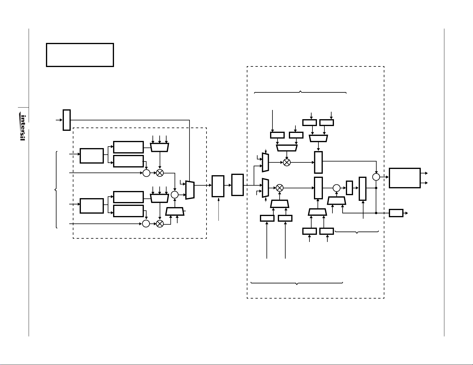
The DCL processes the In-phase (I) and quadrature (Q)
components of a baseband signal which have been digitized
to 10 bits. As shown in the block diagram, the main signal
path consists of a complex multiplier, selectable matched
filters, gain multipliers, cartesian-to-polar converter, and soft
decision slicer. The complex multiplier mixes the I and Q
inputs with the output of a quadrature NCO. Following the
mix function, selectable matched filters are provided which
perform integrate and dump or root raised cosine filtering
(α ~ 0.40). The matched filter output is routed to the slicer,
which generates 3-bit soft decisions, and to the cartesian-topolar converter, which generates the magnitude and phase
terms required by the AGC and Carrier Tracking Loops.
The PLL system solution is completed by the HSP50210
error detectors and second order Loop Filters that provide
carrier tracking and symbol synchronization signals. In
applications where the DCL is used with the HSP50110,
these control loops are closed through a serial interface
between the two parts. To maintain the demodulator
performance with varying signal powerandSNR,aninternal
AGC loop is provided to establish an optimal signal level at
the input to the slicer and to the cartesian-to-polar converter.
3652.4
Features
• Clock Rates Up to 52MHz
• Selectable Matched Filtering with Root Raised Cosine or
Integrate and Dump Filter
• Second Order Carrier and Symbol Tracking Loop
Filters
• Automatic Gain Control (AGC)
• Discriminator for FM/FSK Detection and Discriminator
Aided Acquisition
• Swept Acquisition with Programmable Limits
• Lock Detector
• Data Quality and Signal Level Measurements
• Cartesian to Polar Converter
• 8-Bit Microprocessor Control - Status Interface
• Designed to work with the HSP50110 Digital
Quadrature Tuner
• 84 Lead PLCC
Applications
• Satellite Receivers and Modems
• BPSK, QPSK, 8-PSK, OQPSK, FSK, AM and FM
Demodulators
• Digital Carrier Tracking
• Related Products: HSP50110 Digital Quadrature Tuner,
D/A Converters HI5721, HI5731, HI5741
• HSP50110/210EVAL Digital Demod Evaluation Board
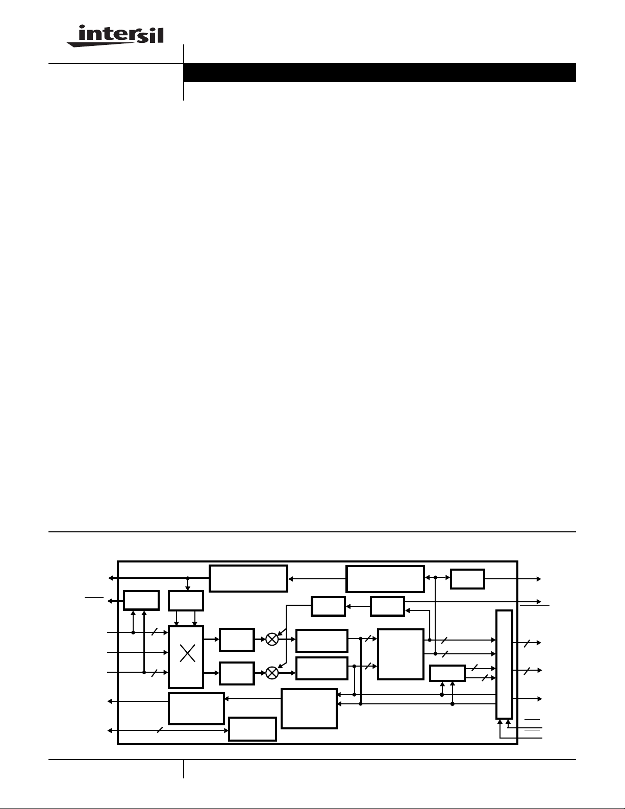
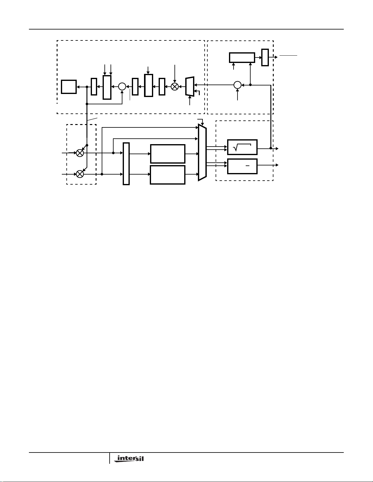
Block Diagram
CARRIER
TRACK
CONTROL
HI/LO
I SER OR
(9-0)
I
IN
SERCLK
OR CLK
Q SER OR
Q
(9-0)
IN
SYMBOL
TRACK
CONTROL
CONTROL/
STATUS
BUS
(COF)
(SOF)
LEVEL
DETECT
COS
10
10
13
3-253
NCO
SIN
I
Q
SYMBOL
TRACKING
LOOP FILTER
CARRIER ACQ/TRK
LOOP FILTER
RRC
FILTER
RRC
FILTER
CONTROL
INTERFACE
CAUTION: These devices are sensitive to electrostatic discharge; follow proper IC Handling Procedures.
CARRIER PHASE
ERROR DETECT
LOOP
FILTER
INTEGRATE/
DUMP
INTEGRATE/
DUMP
SYMBOL
PHASE
ERROR
DETECT
http://www.intersil.com or 407-727-9207
LEVEL
DETECT
8
CARTESIAN
8
TO
POLAR
LOCK
DETECT
MAGNITUDE
8
8
SLICER
PHASE
3
3
Q
I
LKINT
THRESH
A
OUT(9-0)
10
10
B
OUT(9-0)
DATA PATH MULTIPLEXER
SMBLCLK
OEA
OEB
| Copyright © Intersil Corporation 1999
Page 2
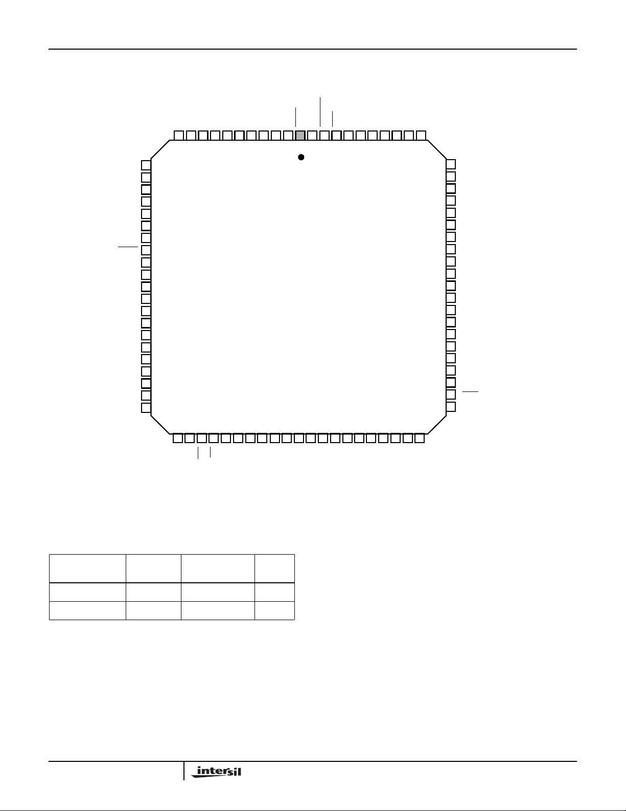
Pinout
IIN6
IIN7
IIN8
IIN9
GND
SERCLK
VCC
SSYNC
HSP50210
84 LEAD PLCC
TOP VIEW
SLOCLK
HI/LO
ISER
QSER
OEA
THRESH
AOUT8
AOUT9
AOUT7
GND
AOUT6
AOUT5
757677787980818283841234567891011
AOUT4
IIN5
IIN4
IIN3
IIN2
GND
IIN1
IIN0
SYNC
QIN9
QIN8
QIN7
QIN6
QIN5
QIN4
VCC
QIN3
QIN2
QIN1
QIN0
SOFSYNC
SOF
12
13
14
15
16
17
18
19
20
21
22
23
24
25
26
27
28
29
30
31
32
WR
COF
COFSYNC
RD
GND
A2
A1
A0
C7
C6
C5
C4
C3
VCC
C2
C1
C0
FZ-ST
FZ-CT
LKINT
535251504948474645444342414039383736353433
GND
74
73
72
71
70
69
68
67
66
65
64
63
62
61
60
59
58
57
56
55
54
AOUT3
AOUT2
AOUT1
AOUT0
SMBLCLK
VCC
CLK
GND
BOUT9
BOUT8
BOUT7
BOUT6
BOUT5
GND
BOUT4
BOUT3
BOUT2
BOUT1
BOUT0
OEB
VCC
Ordering Information
TEMP.
PART NUMBER
RANGE (oC) PACKAGE
HSP50210JC-52 0 to 70 84 Lead PLCC N84.1.15
HSP50210JI-52 -40 to 85 84 Lead PLCC N84.1.15
3-254
PKG.
NO.
Page 3
HSP50210
Pin Description
NAME TYPE DESCRIPTION
V
CC
GND - Ground.
IIN9-0 I In-Phase Parallel Input. Data may be two’s complement or offset binary format (see Table 14). These inputs are
QIN9-0 I Quadrature Parallel Input. Data may be two’s complement or offset binary format (see Table 14). These inputs are
SYNC I Data Sync. When SYNC is asserted “Low”, data on IIN9-0 and QIN9-0 is clocked into the processing pipeline by the
COF O Carrier Offset Frequency. The frequency term generated by the Carrier TrackingLoop Filter is output serially via this
COFSYNC O Carrier Offset Frequency Sync. This signal is asserted one CLK or SLOCLK cycle before the MSB of the serial data
SOF O Sampler Offset Frequency. Sample frequency correction term generatedbytheSymbol TrackingLoopFilterisoutput
SOFSYNC O Sampler Offset Frequency Sync. This signal is asserted one CLK or SLOCLK cycle before the MSB of the serial
A2-0 I AddressBus.Theaddress on these pins specify a target register for reading or writing (see Microprocessor Interface
C7-0 I/O Microprocessor Interface Data Bus. This bi-directional bus is used for reading and writing to the processor interface.
WR I Write. This is the write strobe for the processor interface (see Microprocessor Interface Section).
RD I Read. This is the read enable for the processor interface (see Microprocessor Interface Section).
FZ_ST I Freeze Symbol Tracking Loop. Asserting this pin “high” zeroes the sampling error into the Symbol Tracking Loop
FZ_CT I Freeze Carrier Tracking Loop. Asserting this pin “high” zeroes the carrier Phase Error input to the Carrier Tracking
LKINT O Lock Detect Interrupt. This pin is asserted “high” for at least 4 CLK cycles when the Lock Detector Integration cycle
THRESH O Threshold Exceeded. This output is asserted “low” when the magnitude out of the Cartesian to Polar converter
SLOCLK O Slow Clock. Optional serial clock used for outputting data from the Carrier and Symbol Tracking Loop Filters. The
ISER I In-Phase Serial Input. Serial data input forIn-Phase Data. Data on this pin is shifted in MSB first and is synchronous
QSER I Quadrature Serial Input. Serial data input for Quadrature Data. Data on this pin is shifted in MSB first and is
SSYNC I Serial Word Sync. This input is asserted “high” one CLK before the first data bit of the serial word (see Figure 2).
SERCLK I Serial Clock. May be asynchronous to other clocks. Used to clock in serial data (see Input Controller Section).
AOUT9-0 O A Output. Data on this output depend on the configuration of Output Selector . AOUT9 is the MSB (see Table 42).
BOUT9-0 O B Output. Data on this output depend on the configuration of Output Selector . BOUT9 is the MSB (see Table 42).
SMBLCLK O Symbol Clock. 50% duty cycle clock aligned with soft bit decisions (see Figure 19).
OEA I A Output Enable. This pin is the three-state control pin for the AOUT9-0. When OEA is high, the AOUT9-0 is high
OEB I B Output Enable. This pin is the three-state control pin for the BOUT9-0. When OEB is high, the AOUT9-0 is high
HI/LO 0 HI/LO. The output of the Input Level Detector is provided on this pin (see Input Level Detector Section). This signal
CLK I System Clock. Asynchronous to the processor interface and serial inputs.
- +5V Power Supply.
sampled by CLK when the SYNC signal is active Low. IIN9 is the MSB. See Input Controller Section.
sampled by CLK when the
rising edge of CLK.
pin. The new offset frequency is shifted out MSB first by CLK or SLOCLK starting with the clock cycle after the
assertion of COFSYNC.
word. (Programmable Polarity, see Table 41, bit 11).
serially via this pin. The frequency word is shifted out MSB first by CLK or SLOCLK starting with the clock cycle after
assertion of SOFSYNC.
data word. (Programmable Polarity, see Table 41, bit 12).
Section). A0 is the LSB.
These are the data I/O pins for the processor interface. C0 is the LSB.
Filter (see Symbol Tracking Loop Filter Section).
Loop Filter.
is finished (see Lock Detector Section). Used as an interrupt for a processor. The Lock Detect Interrupt may be
asserted “high” longer than 4 CLK cycles, depending on the Lock Detector mode.
exceeds the programmable Power Detect Threshold (see Table 15 and AGC Section).
clock is programmable and has a 50% duty cycle.
SYNC signal is active Low. QIN9 is the MSB. See Input Controller Section.
Note: Not used when the HSP50110 is used with the
HSP50210 (see Table 41).
to SERCLK (see Input Controller Section).
synchronous to SERCLK (see Input Controller Section).
impedance.
impedance.
can be externally averaged and used to control the gain of an amplifier to close an AGC loop around the A/D converter. This type of AGC sets the level based on the median value on the input.
3-255
Page 4
3-256
HI/LO
SYNC
IIN9-0
QIN9-0
SSYNC
SERCLK
ISER
QSER
LEVEL
DETECT
INPUT CONTROLLER
I
Q
SYNTHESIZER/
MIXER
SIN
COS
NCO
AGC
LOOP
FILTER
MATCHED FILTERING
M
U
X
M
U
X
RRC
RRC
M
U
X
M
U
X
I&D
I&D
GAIN ERROR
DETECT
M
U
X
M
U
X
CARTESIAN
TO
POLAR
I2+Q
Q
TAN-1( )
SLICER
2
I
THRESH
SMBLCLK
SOFSYNC
SOF
COFSYNC
COF
SLOCLK
C7-0
WR
RD
A2-0
CLK
FRZ_ST
FRZ_CT
FORMATTER
8
MICROPROCESSOR
SERIAL
OUTPUT
INTERFACE
SYMBOL TRACKING
SYMBOL PHASE
ERROR DETECT
CARRIER PHASE
ERROR DETECT
DISCRIMINATOR
FREQUENCY
ERROR DETECT
FROM
LOCK
DETECTOR
ACQUISITION
CONTROL
2ND ORDER LOOP
FILTER
CARRIER TRACKING
2ND ORDER LOOP
FILTER
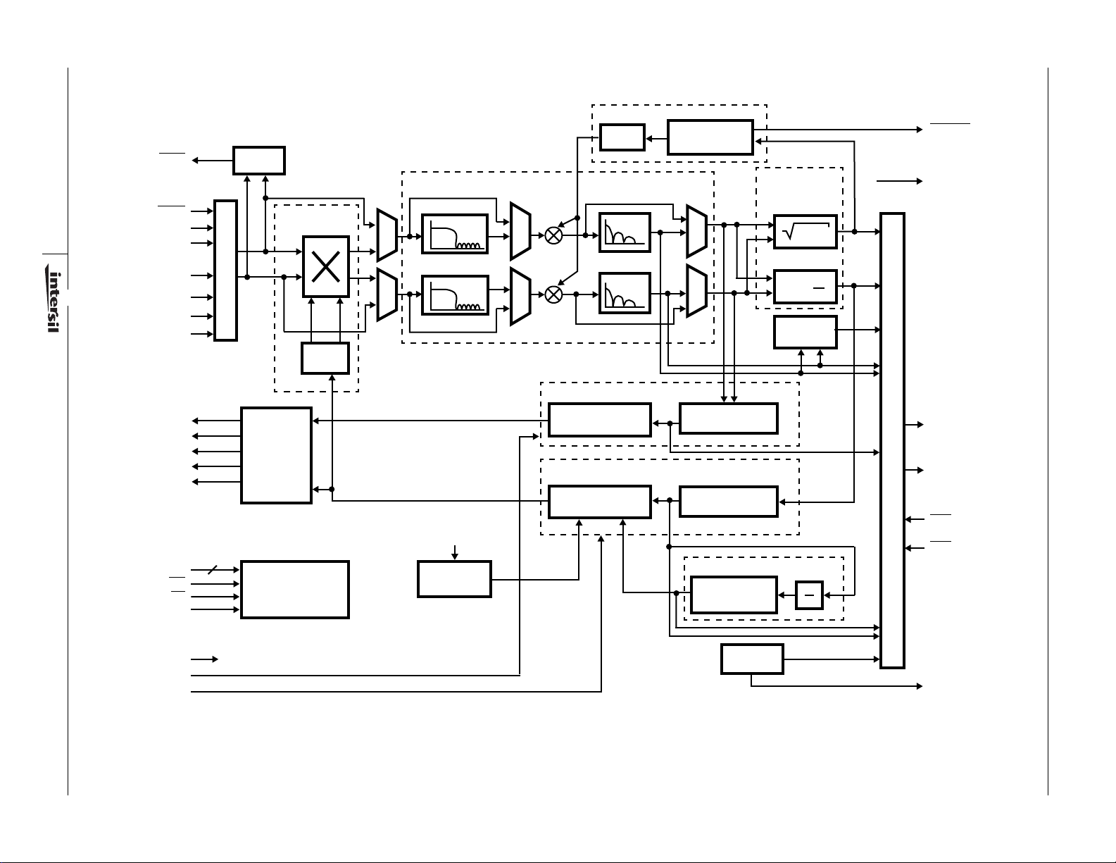
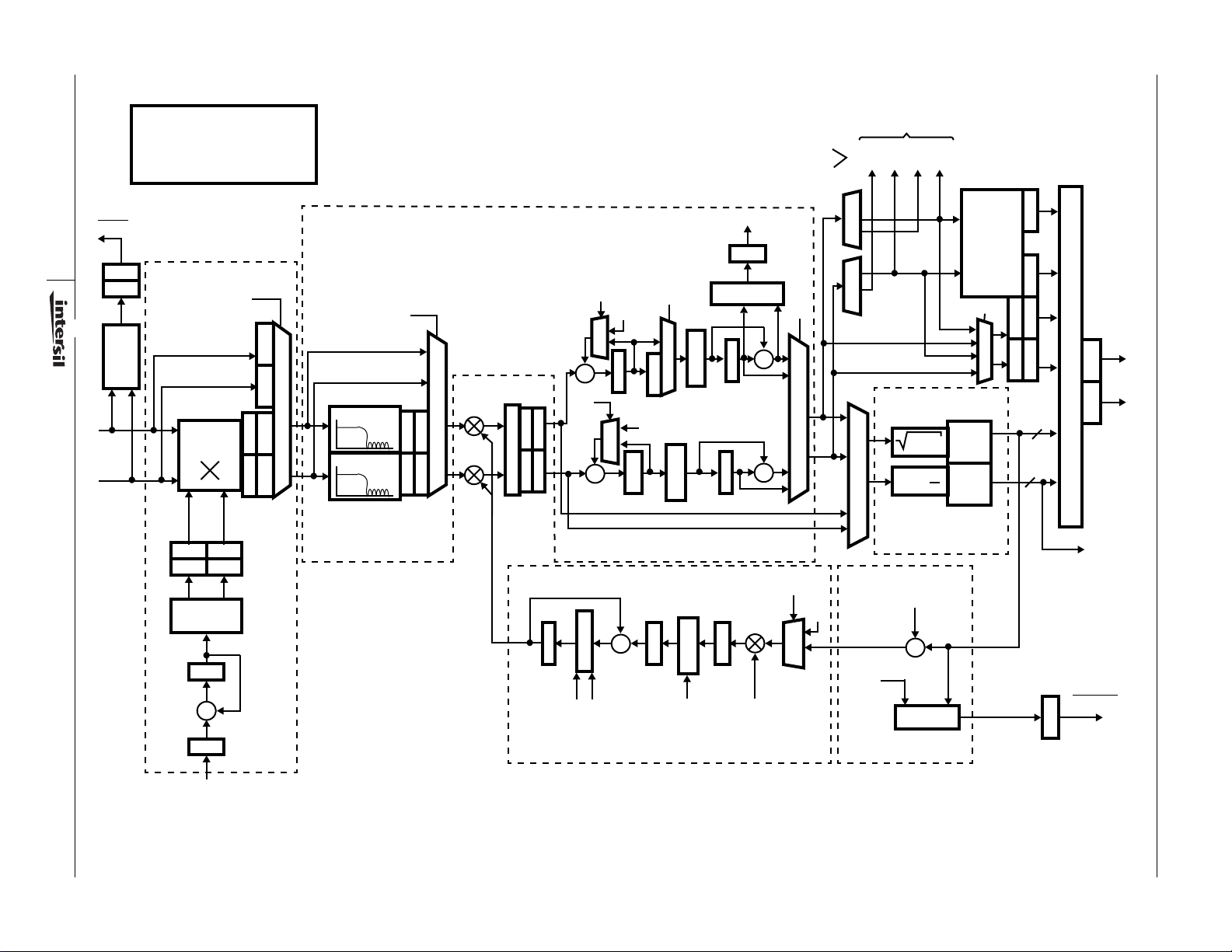
FIGURE 1. FUNCTIONAL BLOCK DIAGRAM OF THE HSP50210
LOCK
DETECT
HSP50210
AOUT9-0
BOUT9-0
OEA
OEB
d
dt
LKINT
Page 5
HSP50210
Functional Description
The HSP50210 Digital Costas Loop (DCL) contains most of
the baseband processing functions needed to implement a
digital Costas Loop Demodulator. These functions include
LO generation/mixing, matched filtering, AGC, carrier phase
and frequency error detection, timing error detection, carrier
loop filtering, bit sync loop filtering, lock detection,
acquisition/tracking control, and soft decision slicing for
forward error correction algorithms. While the DCL is
designed to work with the HSP50110 Digital Quadrature
Tuner (DQT) as a variable rate PSK demodulator for satellite
demodulation, functions on the chip are common to many
communications receivers.
The DCL provides the processing blocks for the three
tracking loops commonly found in a data demodulator: the
Automatic Gain Control (AGC) loop, the Carrier Tracking
Loop, and a Symbol Tracking Loop. The AGC loop adjusts
for input signal power variations caused by path loss or
signal-to-noise variations. The carrier tracking loop removes
the frequency and phase uncertainties in the carrier due to
oscillator inaccuracies and doppler. The symbol tracking
loop removes the frequency and phase uncertainties in the
data and generates a recovered clock synchronous with the
receiveddata. Each loop consists of an error detector,a loop
filter, and a frequency or gain adjustment/control. The AGC
loop is internal to the DCL, while the symbol and carrier
tracking loops are closed external to the DCL. When the
DCL is used together with the HSP50110, the tracking loops
are closed around the baseband filtering to center the signal
in the filter bandwidth. In addition, the AGC function is
divided between the two chips with the HSP50110 providing
the coarse AGC, and the HSP50210 providing the fine or
final AGC.
A top level block diagram of the HSP50210 is shown in
Figure 1. This diagram shows the major blocks and the
multiplexers used to reconfigure the data path for various
architectures.
Input Controller
In-Phase (I) and Quadrature (Q) data enters the part through
the Input Controller. The 10-bit data enters in either serial or
parallel fashion using either two’s complement or offset
binary format. The input mode and binary format is set in the
Data Path Configuration Control Register, bits 14 and 15
(see Table 14).
If Parallel Input mode is selected, I and Q data are clocked
into the part through IIN0-9 and QIN0-9 respectively. Data
enters the processing pipeline when the input enable
(
SYNC) is sampled “low” by the processing clock (CLK). The
enable signal is pipelined with the data to the various
processing elements to minimize pipeline delay where
possible. As a result, the pipeline delay through the AGC,
Carrier Tracking, and Symbol Tracking Loop Filters is
measured in CLKs; not input data samples.
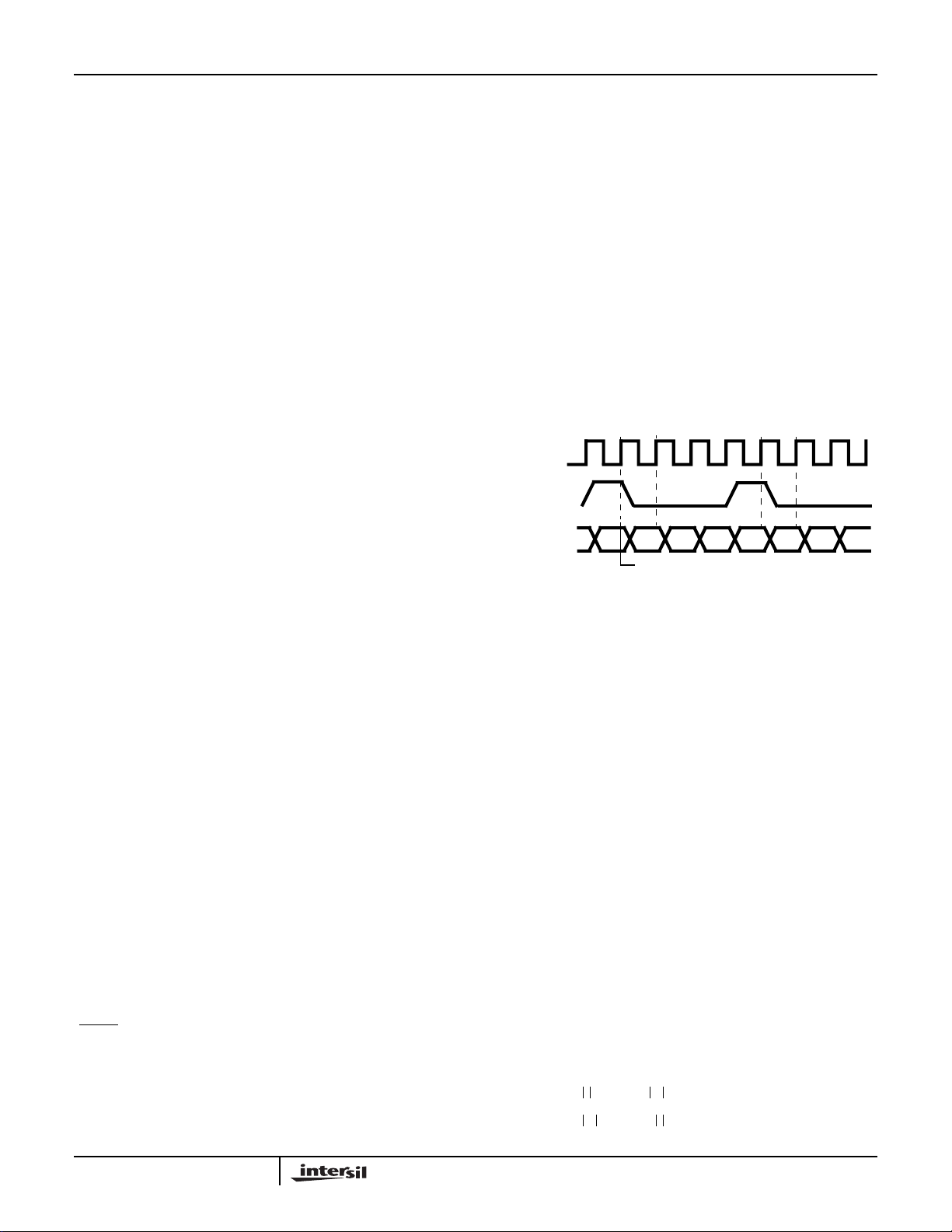
If serial input mode is selected, the I and Q data enters via
the ISER and QSER pins using SERCLK and SSYNC. The
beginning of a serial word is designated by asserting
SSYNC ‘high’ one SERCLK prior to the first data bit, as
shown in Figure 2. On the following SERCLK’s, data is
shifted into the register until all 10 bits havebeen input. Data
shifting is then disabled and the contents of the register are
held until the next assertion of SSYNC. The assertion of a
SSYNC transfers data into the processing pipeline, and the
Shift Register is enabled to accept new data on the following
SERCLK. When data is transferred to the processing
pipeline by SSYNC, a processing enable is generated which
follows the data through the pipeline. This enable allows the
delaythrough processing elements (likethe loop filters) to be
minimized since their pipeline delay is expressed in CLKs
not SSYNC periods.
Note: SSYNC should not be
asserted for more than one SERCLK cycle.
SERCLK
SSYNC
ISER/
QSER
NOTE: Data must be loaded MSB first.
FIGURE 2. SERIAL INPUT TIMING FOR ISER AND QSER INPUTS
MSB
SSYNC LEADS 1st DATA BIT
MSB
Input Level Detector
The Input Level Detector generates a one-bit error signal for
an external IF AGC filter and amplifier. The error signal is
generated by comparing the magnitude of the input samples
to a user programmable threshold. The HI/LO pin is then
driven “high” or “low” depending on the relationship of its
magnitude to the threshold. The sense of the HI/LO pin is
programmable so that a magnitude exceeding the threshold
can either be represented as a “high” or “low” logic state.
The Input Level Detector (HI/LO output) threshold and the
sense are set by the Data Path Configuration Control
Register bits 16-23 and 13 (see Table 14).
Level Detector is typically not used in applications
which use the HSP50210 with the HSP50110.
The high/low outputs can be integrated by an external loop
filter to close an AGC loop. Using this method, the gain of
the loop forces the median magnitude of the input samples
to the threshold. When the magnitude of half of the samples
is above the threshold (and half is below), the error signal is
integrated to zero by the loop filter.
The magnitude of the complex input is estimated by:
Mag (I, Q) I 0.375 Q if I Q and>×+=
Mag (I, Q) Q 0.375 I if Q I>×+=
Note: The Input
(EQ. 1)
3-257
Page 6
REGISTER ENABLE RATE
@ = SYNC RATE
= TWICE SYMBOL RATE
*
! = SYMBOL RATE
BLANK = CLK RATE
MID AND END
SYMBOL SAMPLES
TO SYMBOL TRACKING
I
MID
I
END
Q
MID
Q
END
3-258
HI/LO
REG
REG
DETECT
IIN9-0QIN9-0
LEVEL
NCO MIXER
COMPLEX
MULTIPLY
SIN
REG REG
REG REG
SIN/COS
ROM
REG
REG
BYPASS
MIXER
COS
+
R
E
G
R
E
G
R
R
E
E
G
G
R
R
E
E
G
G
CF
REGISTER
MATCHED FILTERING
M
U
X
15 TAP RRC
@
15 TAP RRC
@
ROOT RAISED COSINE
BYPASS
RRC
(RRC)
D
FALSE LOCK
REG
DATA DE-SKEW
DUMP
+
M
U
R
R
X
E
E
G
G
R
R
E
E
G
G
R
L
E
I
G
M
R
I
E
T
G
DUMP
R
E
G
R
E
G
AGC LOOP FILTER
R
E
G
@ OR !
UPPER
GAIN
LIMIT
+
L
I
M
I
T
LOWER
GAIN
LIMIT
OQPSK
“0”
M
U
X
R
E
G
M
U
X
M
U
R
X
E
G
@
*
“0”
S
R
H
E
F
G
T
@
INTEGRATE AND DUMP
R
E
+
G
LOOP GAIN
EXPONENT
COMPARE
S
R
H
I
E
F
G
T
*
TWO SAMPLE
SUMMER
R
I
E
G
*
S
R
H
E
I
G
F
T
LOOP GAIN
MANTISSA
BYPASS
I&D
+
M
U
X
+
HOLD AGC
M
U
X
E
M
U
X
D
E
M
U
X
M
U
X
AGC ERROR DETECT
“0”
AGC THRESHOLD
GAIN
ERROR
POWER
THRESHOLD
CARTESIAN TO
POLAR
2
I2+Q
Q
-1
TAN
( )
I
PHASE OUT AT
MAG OUT AT
-
+
COMPARE
SOFT
DECISION
SLICER
TEST
5
DELAY
REG
5
DELAY
REG
@ OR
@ OR !
M
U
X
R
E
G
R
E
G
R
E
G
R
E
G
O
R
U
E
T
**
G
P
R
U
! OR ! OR
E
T
G
S
E
L
E
8
C
T
8
AOUT9-0 BOUT9-0
R
E
G
R
E
G
HSP50210
*
TO
CARRIER
TRACKING
AND
DISCRIMINATOR
THRESH
R
E
G
FROM CARRIER TRACKING
LOOP FILTER
FIGURE 3. MAIN DATA PATH
Page 7

HSP50210
NCO/Mixer
The NCO/Mixer performs a complex multiply between the
baseband input and the output of a quadrature NCO
(Numerically Controlled Oscillator). When the HSP50210
(DQT) is used with the HSP50110 (DCL), the NCO/Mixer
shortens the Carrier Tracking Loop (i.e., minimizes pipeline
delay around the loop) while providing wide loop
bandwidths. This becomes important when operating at
symbol rates near the maximum range of the part.
There are three configurations possible for closing the
Carrier Tracking Loop when the DQT and the DCL are used
together.The first configuration utilizes the NCO on the DQT
and bypasses the NCO in the DCL. The Data Path
Configuration Control Register (see Table 14), bit 10, and
Carrier Loop Filter Control Register #1 (see Table 20), bit 6,
are used to bypass the DCL NCO/Mixer and route the Loop
filter outputs, respectively. The DQT provides maximum
flexibility in NCO control with respect to frequency and
phase offsets.
The second configuration feeds the lead Carrier Loop filter
term to the DCL NCO/Mixer, and the lag Loop filter Term to
the DQT NCO. This reduces the loop transport delay while
maintaining wide loop bandwidths and reasonable loop
damping factors. This configuration is especially useful in
SATCOM applications with medium to high symbol rates.
The Carrier Loop Filter Control Register #1, bit 5, is where
the lead/lag destination is set.
The final configuration feeds both the lead and lag Carrier
Loop Filter terms back to the DCL NCO/Mixer. This provides
the shortest transport delay. The DCL NCO/Mixer provides
only for frequency/phase control from the Carrier Loop filter.
The center frequency of this NCO/Mixer is set to the average
of the Upper and Lower Carrier Loop Limits programmable
parameters. These parameters are set in the two control
registers bearing their names (see Tables 22 and 23).
The NCO/Mixer uses a complex multiplier to multiply the
baseband input by the output of a quadrature NCO. This
operation is represented by:
I
OUTIIN
Q
OUTIIN
Equation 3 illustrates how the complex multiplier implicitly
performs the summing function when the DCL is configured
as a modulator. The quadrature outputs of the NCO are
generated by driving a sine/cosine look-up table with the
output of a phase accumulator as shown in Figure 3. Each
time the phase accumulator is clocked, its sum is
incremented by the contents of the Carrier Frequency (CF)
Register. As the accumulator sum increments from 0 to 2
the SIN/COS ROM produces quadrature outputs whose
phase advances from 0 to 360
32-bit phase increment which is updated with the output of
ωC()cos Q
ωC()sin Q
IN
ωC()sin–=
ωC()cos+=
IN
o
. The CF Register contains a
(EQ. 2)
(EQ. 3)
32
Carrier Tracking Loop. Large phase increments take fewer
clocks to step through the sine wave cycle, which results in a
higher frequency NCO output.
The CF Register sets the NCO frequency with the following
equation:
FCf
CF INT FCf
where f
CF()2⁄
×=
CLK
[]H=
is the CLK frequency, and CF is the 32-bit two’s
CLK
32
⁄()2
CLK
32
(EQ. 4)
complement hexadecimal value loaded into the Carrier
Frequency Register. As an example, if the CF Register is
loaded with a value of 4000 0000 (Hex), and the CLK
frequency is 40MHz, the NCO would produce quadrature
terms with a frequency of 10MHz. When CF is a negative
value, a clockwise cos/sin vector rotation is produced. When
CF is positive, a counterclockwise vector rotation is
produced.
NOTE: The NCO is set to a fixed frequency by programming the
upper and lower limits of the Carrier Tracking Loop Filter to the
same value and zeroing the lead gain.
Matched Filtering
The HSP50210 provides two selectable matched filters: a
Root Raised Cosine Filter (RRC) and an Integrate and
Dump (I&D) filter. These are shown in Figure 3. The RRC
filter is provided for shaped data pulses and the I&D filter is
provided for square wave data. The filters may be cascaded
for better adjacent channel rejection for square wave data. If
these two filters do not meet baseband filtering
requirements, then they can be bypassed and an external
digital filter (such as the HSP43168 Dual FIR Filter or the
HSP43124 Serial I/O Filter) used to implement the desired
matched filter. The desired filter configuration is set in the
Data Path Configuration Control Register, bits 1-7 (see
Table 14).
The sample rate of the baseband input depends on the
symbol rate and filtering configuration chosen. In
configurations which bypass both filters or use only the RRC
Filter,the input sample rate must be twice the symbol rate. In
configurations which use the I&D Filter,the input sample rate
is decimated by the I&D Filter, down to two samples per
symbol. I&D configurations support input sample rates up to
32 times the input symbol rate.
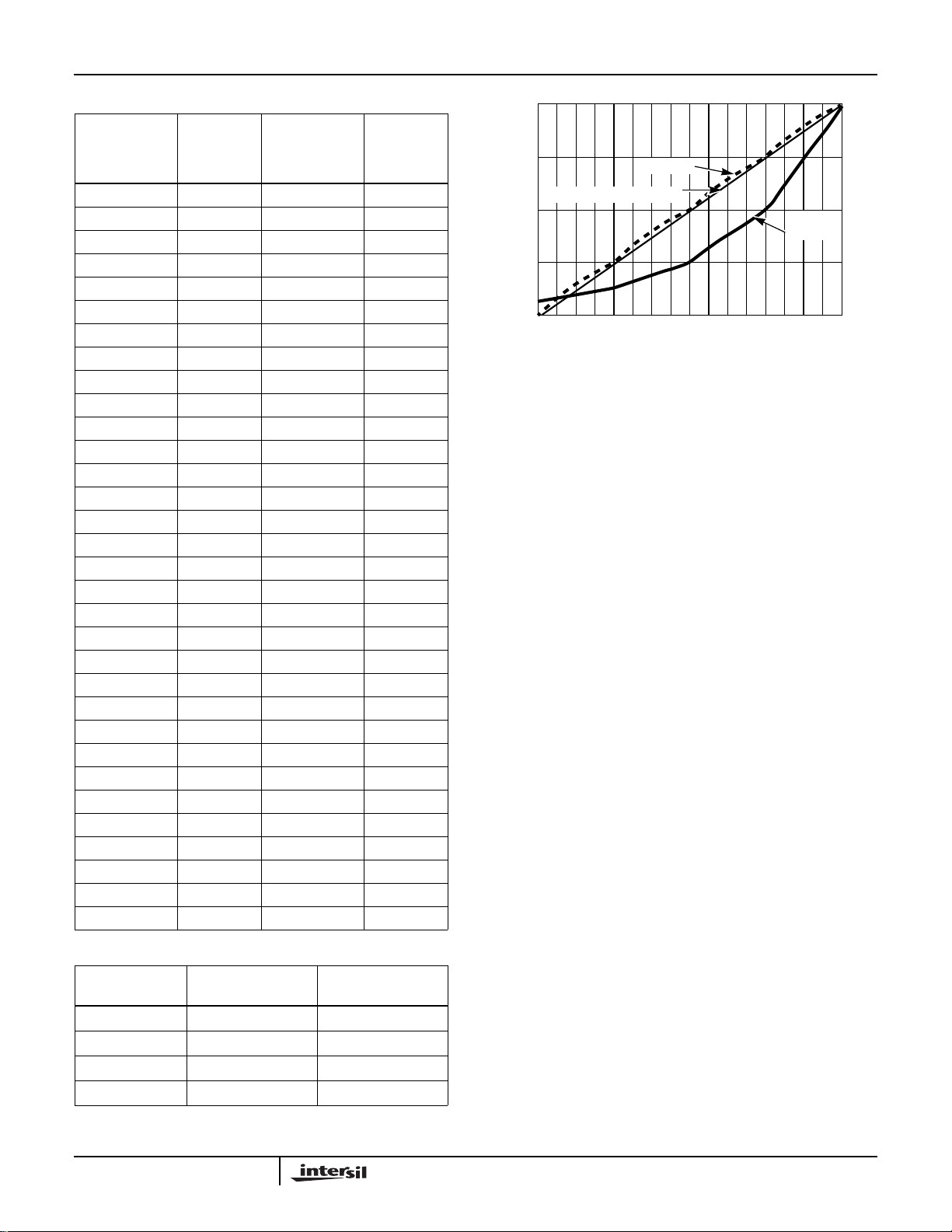
The RRC filter is a fixed coefficient 15 Tap FIR filter. It has
~40% excess bandwidth beyond Nyquist which equates to
α = ~0.4 shape factor. The filter frequency response is
shown in Figure 4 and Figure 5. In addition, the 9-bit filter
,
coefficients are listed as integer values in Table 1. The noise
equivalent bandwidth of the RRC filter and other filter
configurations possible with the HSP50110/210 chipset are
given in Appendix A.
3-259
Page 8
HSP50210
0
-20
-40
-60
-80
NORMALIZED MAGNITUDE (dB)
-100
0
f
CLK
10
FREQUENCY (NORMALIZED TO INPUT SAMPLE RATE)
2f
CLK
10
3f
CLK
10
FIGURE 4. RRC FILTER IN HSP50210
0
-0.18
-0.36
SHOWN BELOW
-0.54
-0.72
NORMALIZED MAGNITUDE (dB)
-0.90
0
0
-0.07
-0.14
-0.21
-0.28
NORMALIZED MAGNITUDE (dB)
-0.35
0
FREQUENCY (NORMALIZED TO INPUT SAMPLE RATE)
ENLARGED FOR CLARITY
f
CLK
2f
CLK
25
3f
20
f
CLK
f
CLK
25
40
CLK
40
3f
CLK
25
f
CLK
10
TABLE 1. ROOT RAISED COSINE COEFFICIENTS
COEFFICIENT INDEX COEFFICIENT
02
1-2
21
38
4 -16
5 -14
4f
CLK
10
f
CLK
2
686
7 160
886
9 -14
10 -16
11 8
12 1
13 -2
14 2
The I&D filter consists of an accumulator, a programmable
shifter and a two sample summer as shown in Figure 3. The
programmable shifter is provided to compensate for the gain
introduced by the accumulator (see Table 14). The
accumulator provides Integrate and Dump Filtering for
decimation factors up to 16. The two sample summer
4f
CLK
25
f
CLK
5
provides the moving average required for an additional
decimation factor of 2. A decimation factor of 1 (bypass), 2,
4, 8, 16, or 32 may be selected. At the maximum decimation
rate, a baseband signal sampled at 32 times the symbol rate
can be filtered.
The output of the two sample summer is demultiplexed into
two sample streams at the symbol rate. The demultiplexed
data streams from the I and Q processing paths are fed to
the Symbol Tracking Block and Soft decision slicer. The
multiplexed data streams on I and Q are provided as one of
the selectable inputs for the Cartesian to Polar Converter.
Cartesian/Polar Converter
3f
5f
CLK
40
CLK
20
The Cartesian/PolarConverter maps samples on the I and Q
processing paths to their equivalent phase/magnitude
representation. The magnitude conversion is equivalent to:
FIGURE 5. PASSBAND RIPPLE OF RRC FILTER IN HSP50210
3-260
Mag (I, Q) 0.81()∗I2Q2+(),=
(EQ. 5)
where 0.81 is the gain of the conversion process. The
magnitude output is an 8-bit unsigned value ranging from 0.0
to 1.9922.
Page 9
HSP50210
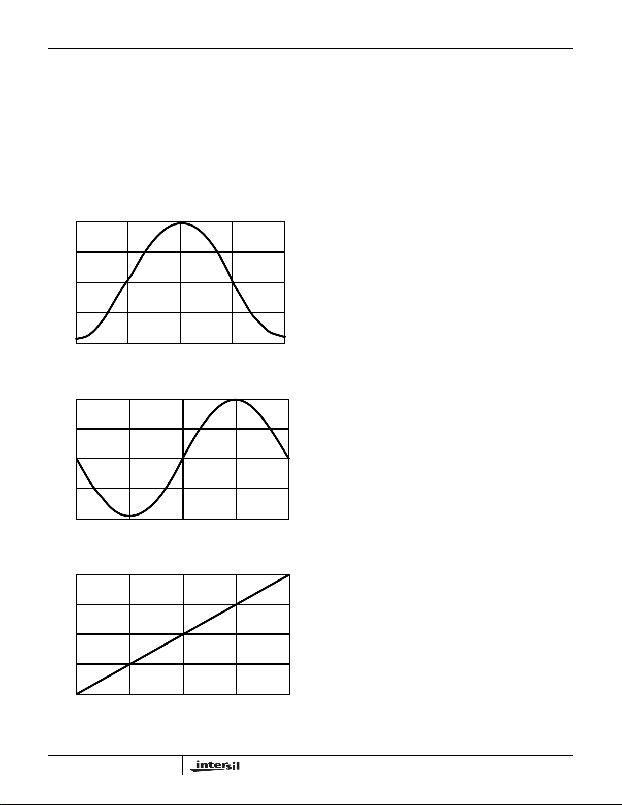
The phase conversion is equivalent to:
Phase (I, Q) tan
where tan
-1
( ) is the arctangent function. The phase
1–
QI⁄(),=
(EQ. 6)
conversion output is an 8-bit two’s complement output which
ranges from -1.0 to 0.9922 (80 to 7f HEX, respectively). The
-1 to almost 1 range of the phase output represents phase
values from -πto π, respectively. An example of the I/Q to
phase mapping is shown in Figure 6. The phase and
magnitude values may be output via the Output Selector bits
0-3 (see Table 42).
1.0
0.5
0
MAGNITUDE
-0.5
-1.0
-π
FIGURE 6A. I INPUT TO CARTESIAN/POLAR CONVERTER
1.0
0.5
0
MAGNITUDE
-0.5
-1.0
-π
FIGURE 6B. Q INPUT TO CARTESIAN/POLAR CONVERTER
1.0
0.5
0
OUTPUT VOLTAGE
-0.5
-1.0
-π
FIGURE 6C. CARTESIAN/POLAR CONVERTER PHASE OUTPUT
-π/2
-π/2
-π/2
0
INPUT PHASE
0
INPUT PHASE
0
INPUT PHASE
π/2
π/2
π/2
The I/Q data path selected for input to the Cartesian to Polar
converter determines the input data rate of the AGC and
carrier tracking loops. If the I/Q data path out of the Integrate
and Dump Filter is selected, the AGC is fed with magnitude
values produced by the end-symbol samples. Magnitude
values produced by midsymbol samples are not used
because these samples occur on symbol transitions, resulting
in poor signal magnitude estimates. The Carrier Tracking
block is fed with phase values generated from both the end
and mid-symbol samples. The carrier tracking loop filter ,
howev er, is only fed with Phase Error terms generated by the
end symbol samples. If the input of the I&D is selected for
input to the coordinate converter, the control loops are f ed
with data at the I/Q data rate. The desired data path input to
the Cartesian to Polar converter is specified in the Data Path
Configuration Control Register, bit 8 (see Table 14).
AGC
The AGC loop operates on the main data path (I and Q) and
performs three signal level adjusting functions: 1)
maximizing dynamic range, 2) compensating for SNR
variations, and 3) maintaining an optimal level into the Soft
Decision Slicer. The AGC Loop Block Diagram, shown in
π
π
π
Figure 7, consists of an Error Detector, a Loop Filter, and
Signal Gain Adjusters (multipliers). The AGC Error Detector
generates an error signal by subtracting the programmable
AGC threshold from the magnitude output of the Cartesian
to Polar Converter. This difference signal is scaled (gain
adjusted via multiplier and shifter), then filtered (integrated)
by the AGC Loop Filter to generate the gain correction to the
I and Q signals at the multipliers. If a fixed gain is desired,
set the upper and lower limits equal.
The AGC responds to the magnitude of the sum of all the
signals in the bandpass of the narrowest filter preceding the
Cartesian to Polar Coordinate Converter. This filter may be
the Integrate and Dump filter shown in Figure 8, the RRC
filter upstream in the HSP50210 data path, or some other
filter outside the DCL chip. The magnitude signal usually
contains several components: 1) the signal of interest
component, 2) the noise component, and 3) interfering
signals component. At high SNR’s the signal of interest is
significantly greater than the other components. At lower
SNR’s, components 2 or 3 may become greater than the
signal of interest. Narrowing the filter bandwidth is the
primary technique used to mitigate magnitude contributions
of component 3. This will also improve the SNR by
reducing the magnitude contributions of element 2.
Consideration of the range of signal amplitudes expected
into the HSP50210, in conjunction with a gain distribution
analysis, will provide the necessar y insight to set the signal
level into the Soft Decision Slicer to yield optimum
performance.
Note: Failure to consider the variations
due to noise or interfering signals, can result in signal
limiting in the HSP50210 processing algorithms, which
will degrade the system Bit Error Rate performance.
3-261
Page 10
HSP50210
The AGC Loop is configured by the PowerDetect Threshold
and AGC Loop Parameters Control Registers (see Tables 15
and 16). Seven programmable parameters must be set to
configure the AGC Loop and its status outputs. Two
parameters, the Power Threshold and the AGC Threshold
are associated with the Error Detector and are represented
in 8-bit fractional unsigned binary format: 2
-7.
5
2-62
. While the format provides a range from 0 - 1.9961
0.2-12-22-32-42-
for the thresholds, the Cartesian to Polar Converter scales
the I and Q input magnitudes by 0.81. Thus, if a full scale
(±1) complex (I and Q) input signal is presented to the
converter,the output will be √(0.81)
2
+ (0.81)2= 1.1455. The
AGC Threshold parameter value is the desired magnitude of
the signal as it enters the Soft Decision Slicer. It is the
parameter that will determine the error signal in the AGC
loop. The Power Threshold, on the other hand, determines
only the power threshold at which the
THRESH signal is
asserted. If the signal magnitude exceeds the threshold,
then the
THRESH is asserted. This may be used for signal
detection, power detection or external AGC around the A/D
converter. The AGC Threshold parameter is set in the AGC
Loop Parameters Control Register,bits 16-23 (see Table 16).
The Power Threshold parameter is set in the Power Detect
Threshold Control Register, bits 0-7 (see Table 15). Note
that these two threshold parameters are not required to be
set to identical or even related values, since they perform
independent functions
The Enable AGC parameter sets the AGC Error Detector
output to zero if asserted and to normal error detection
output when not asserted. This control bit is set in the AGC
Loop ParameterControl Register, bit 31 (see Table 16). This
bit is used to disable the AGC loop.
The remaining AGC parameters determine the AGC loop
characteristics: gain tracking, tracking rate and tracking limits.
The AGC Loop gain is set via two parameters: A GC Loop
Gain Exponent and AGC Loop Gain Mantissa. In general, the
higher the loop gain, the faster signal level acquisition and
tracking, but this must be tempered b y the specific signal
characteristics of the application and the remaining
programmable loop parameters. For the HSP50210, the AGC
Loop Gain provides for a variab le atten uation of the input to
the loop filter. The A GC gain mantissa is a 4-bit value which
provides error signal scaling from 0.000 to 0.9375, with a
resolution of 0.0625. Table 2 details the discrete set of
decimal values possible forthe AGC Loop Gain mantissa. The
-7
exponent provides a shift factor scaling from 2
to 2
-14
.
Table 3 details the discrete set of decimal values possible for
the AGC Loop Gain Exponent. When combined, the exponent
and mantissa provide a loop gain defined as:
AGC Loop Gain: G
AGC
M()24–()[]2
()[]=
7E+()–
(EQ. 7)
Register, bits 24-30 (see Table 16). The composite range of
the AGC loop Gain is 0.0000 to [0.9375][2-7]. This will scale
the AGC error signal to a range of 0.000 to
(1.1455)(0.9375)(2-7) = 1.07297(2-7).
TABLE 2. AGC LOOP GAIN BINARY MANTISSA TO DECIMAL
SCALED MANTISSA MAPPING
BINARY
CODE
(MMMM)
0000 0.0000 1000 0.5000
0001 0.0625 1001 0.5625
0010 0.1250 1010 0.6250
0011 0.1875 1011 0.6875
0100 0.2500 1100 0.7500
0101 0.3125 1101 0.8125
0110 0.3750 1110 0.8750
0111 0.4375 1111 0.9375
TABLE 3. AGC LOOP BINARY EXPONENT TO SCALED
BINARY CODE
(EEE)
000 0 2
001 1 2
010 2 2
011 3 2
100 4 2
101 5 2
110 6 2
111 7 2
DECIMAL
SCALED
MANTISSA
DECIMAL EXPONENT MAPPING
DECIMAL/ HEX
EXPONENT
BINARY
CODE
(MMMM)
DECIMAL SCALED
DECIMAL
SCALED
MANTISSA
EXPONENT
-7
-8
-9
-10
-11
-12
-13
-14
where M is a binary number with a range from 0 to 15 and E
is a 3-bit binary value from 0 to 7. M and E are the
parameters set in the AGC Loop Parameters Control
3-262
Page 11
HSP50210
READ
REG
AGC GAIN = (1.0 + M) x 2
GAIN
ADJUST
G
AGC
I
Q
AGC LOOP FILTER
AGC
AGC
UPPER
E
LOWER
LIMIT †
LIMIT †
L
R
I
E
M
G
I
T
1.0000 TO 15.8572 = G
(0 TO 24dB)
AGC LOOP
GAIN
MANTISSA †
-7
TO 2
(2
S
R
H
I
E
+
0.000 TO 1.07297(2
L
I
M
I
T
F
G
T
AGC
CART/POLAR INPUT SELECT†
AGC LOOP
EXPONENT †
-14
(0.000 TO 0.9375)
)
R
E
G
-7
)
I&D FILTER
I&D FILTER
GAIN
M
U
X
“0”
ENABLE AGC †
M
U
X
AGC ERROR DETECT
COMPARE
POWER
THRSHLD †
+
G
TAN
-
1.64
-----------=
I2+Q
-1
( )
GAIN
ERROR
AGC THRSHLD †
CARTESIAN TO POLAR
1.0
R
E
THRESH
G
1.64
dcloutlvl agc thresh
=
----------- -
2
where dcloutlvl is the
2
2
Q
I
magnitude output expressed
in dB from Full Scale (dBFS)
0.8
MAGNITUDE
(0 - 1.1455)
PHASE
† Indicates a microprocessor control signal.
FIGURE 7. AGC LOOP BLOCK DIAGRAM
The AGC Loop Filter integrates the scaled error signal to
provide a correction control term to the multipliers in the I and
Q path. The loop filter accumulator has internal upper and
lower limiters. The upper eight bits of the accumulator output
map to an exponent and mantissa format that is used to set
these upper and lower limits. The format, illustrated in Figure
8, is used for the AGC Upper Limit, AGC Lower Limit and the
Correction Control Term(AGC output). This format should not
be confused with the similar format used for the AGC Loop
Gain. The input to the AGC Loop Filter is included in Figure 8
to show the relative weighting of the input to output of the loop
filter. The loop filter input is represented as the ele ven letter
“G”s. Lower case “e” and “m” detail the format f or the AGC
Upper and LowerLimits. This change in type case should help
keep the AGC Limits and A GC Gain formats from being
confused. The AGC Upper and Lower Limits are set in the
AGC Loop Parameters Control Register, bits 0-15, (see Table
16). This 6-bit unsigned mantissa format provides for an AGC
output control range from 0.0000 to 0.9844, with a resolution
of 0.015625. The 2-bit exponent format provides an A GC
output control range from 1 to 8. The decimal values for each
of the 64 binary mantissa values is detailed in Table 4, while
Table 5 details the decimal value for the 4 exponent values .
The AGC Output is implemented in the multiplier according
to Equation 8.
Out
Out
AGC linear–
AGC dB–
1.0 m
+()2e()=
AGC
20 log 1.0 m
+()2e()[]=
AGC
(EQ. 8A)
(EQ. 8B)
where m and e are the binary values for mantissa and
exponent found in Tables 4 and 5.
NOTE:Thisformat is identical to the format used to program the
AGC Upper and Lower Limits, but in this usage it is not a programmed value. It is a representation of the digital AGC output
number which is presented to the Gain Adjuster (multipliers) to
correct the gain of the I and Q data signals in the main data path.
These equations yield a composite (mantissa and
exponent) AGC output range of 0.0000 to 1.9844(2
3
) which
is a logarithmic range from 0 to 24dB. Figure 9 has graphed
the results of Equation 8 for both the linear and logar ithmic
equations. Figure 9 also has a linear estimate of the
logarithmic equation. This linear approximation will be used
in calculating the AGC response time.
120.2-12-22-32-42-52-62-72-82-92-102-112-122-132-142-152-162-172-18
2
ee.mmmmm m
GGGG GGGGGG G
FIGURE 8. AGC OUTPUT AND AGC LIMITS BIT WEIGHTING
3-263
Page 12
HSP50210
TABLE 4. AGC GAIN MANTISSA TO DECIMAL MAPPING
DECIMAL
VALUE
BINARY CODE
(MMMMMM
TABLE 5. AGC GAIN EXPONENT TO DECIMAL MAPPING
BINARY CODE
AGC
000000 0.000000 100000 0.500000
000001 0.015625 100001 0.515625
000010 0.031250 100010 0.531250
000011 0.046875 100011 0.546875
000100 0.062500 100100 0.562500
000101 0.078125 100101 0.578125
000110 0.093750 100110 0.593750
000111 0.109375 100111 0.609375
001000 0.125000 101000 0.625000
001001 0.140625 101001 0.640625
001010 0.156250 101010 0.656250
001011 0.171875 101011 0.671875
001100 0.187500 101100 0.687500
001101 0.203125 101101 0.703125
001110 0.218750 101110 0.718750
001111 0.234375 101111 0.734375
010000 0.250000 110000 0.750000
010001 0.265625 110001 0.765625
010010 0.281250 110010 0.781250
010011 0.296875 110011 0.796875
010100 0.312500 110100 0.812500
010101 0.328125 110101 0.828125
010110 0.343750 110110 0.843750
010111 0.359375 110111 0.859375
011000 0.375000 111000 0.875000
011001 0.390625 111001 0.890625
011010 0.406250 111010 0.906250
011011 0.421875 111011 0.921875
011100 0.437500 111100 0.937500
011101 0.453125 111101 0.953125
011110 0.468750 111110 0.968750
011111 0.484375 111111 0.984375
00 0 2
01 1 2
10 2 2
11 3 2
OF AGC
)
MANTISSA
BINARY CODE
(MMMMMM
DECIMAL/ HEX
EXPONENT
DECIMAL SCALED
)
AGC
EXPONENT
DECIMAL
VALUE
OF AGC
MANTISSA
0
1
2
3
224
240
24
18
12
6
0
256
16
12
LINEAR ESTIMATE IN dB
8
4
DATA PATH GAIN (LINEAR)
1
0
0
1632486480
(8 MSBs OF LOOP FILTER ACCUMULATOR)
FIGURE 9. GAIN CONTROL TRANSFER FUNCTION
GAIN dB
96
112
128
144
GAIN CONTROL WORD
160
176
192
GAIN
LINEAR
208
There are two techniques for setting a fixed gain for the
AGC. The first is to set Control Word 2 bit 31 = 1. This
precludes any error update of present AGC gain value.The
second is to set the upper and lower AGC limits to the
desired gain using Figure 9. The upper and lower limits
have the same value for this case.
The HSP50210 provides two mechanisms for monitoring
signal strength. The first, which involved the THRESH
signal, has already been described. The second
mechanism is via the Microprocessor Interface. The 8 most
significant bits of the AGC loop filter output can be read by
a microprocessor. Refer to the Microprocessor Interface
Section for details of how to read this value. This AGC
value has the format described in Figure 8.
AGC Bit Weighting and Loop Response
The AGC loop response is a function of the programmable
gain, the bit weightings inherent in the connection of each
element of the loop, the AGC Loop filter limits and the
magnitude of the input gain error step. Table 6 details the bit
weighting between each element of the AGC Loop from the
error detector through the weighting at the gain adjuster in
the signal path. The AGC Loop Gain sets the growth rate of
the sum in the loop filter accumulator. The Loop filter output
growth rate determines how quickly the AGC loop traces the
transfer function shown previously in Figure 9. To calculate
the rate at which the AGC can adjust over a given period of
time, a gain step is introduced to the gain error detector and
the amount of change that is observed between clocks at the
AGC Level Adjusters (multipliers) is the AGC response time
in dB per symbol.This AGC loop will respond immediately
with the greatest correction term, then asymptotically
approach zero correction.
We begin calculation of the loop response with a full scale
error detector input of ±1. This error input is scaled by the
Cartesian to Polar converter, the error detector and the AGC
Loop Gain, accumulated in the loop filter,limited and output to
the gain adjusters. The AGC loop tries to make the error
correction as quickly as possible, but is limited by the AGC
GAIN (dB)
3-264
Page 13
HSP50210
Loop Gain and potentially,the AGC limits. The maximum AGC
response is the maximum gain adjustment made in any given
clock cycle. This inv olves applying maximum Loop gain and
setting the AGC limits as wide as possible. A calculation using
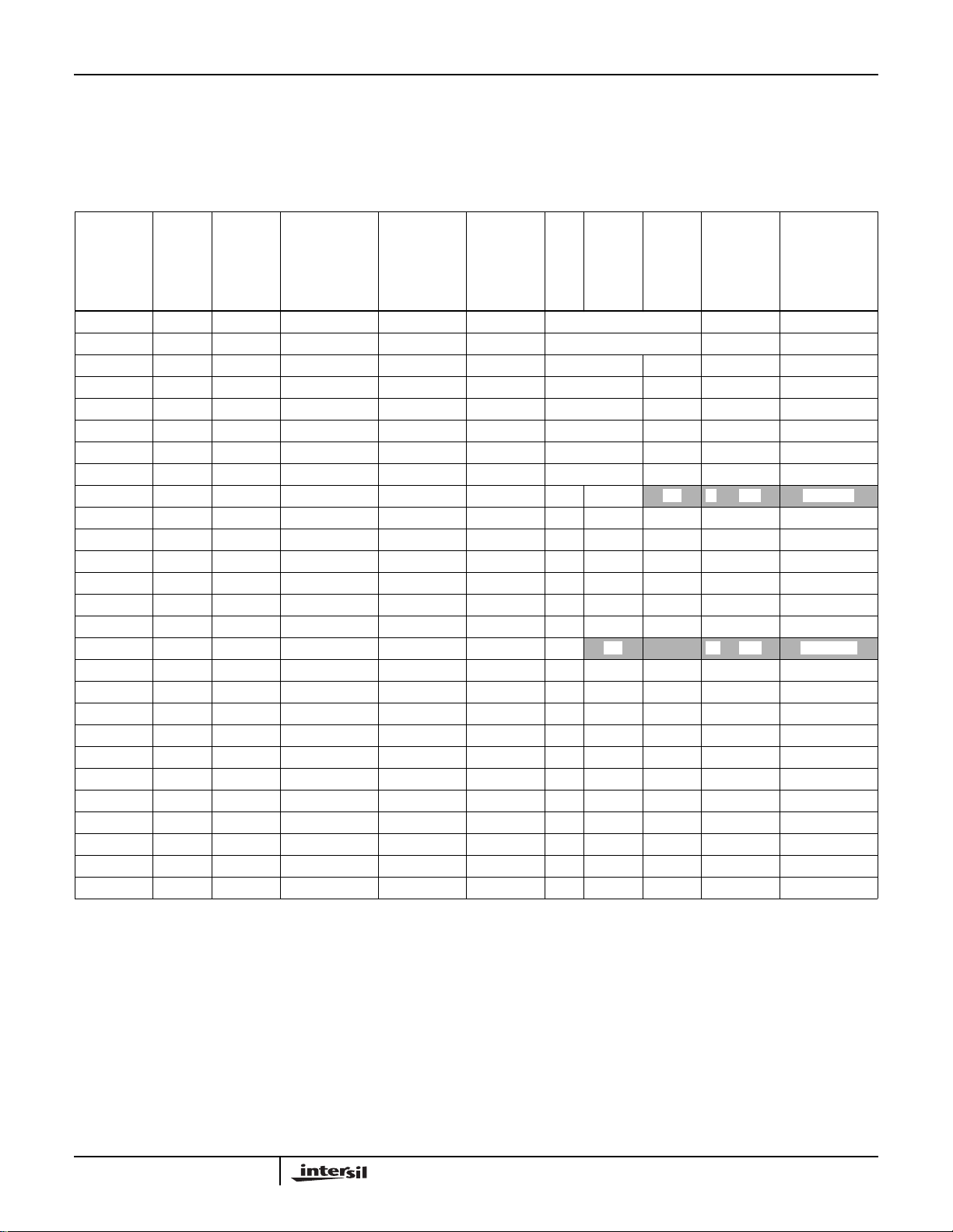
TABLE 6. AGC BIT WEIGHTING
AGC LOOP
AGC
ACCUM
BIT
POSITION
22 Shifter → E1 12
21 Shifter → E0 6
20 Multiplier → M-1 3
19 M -2 1.5
18 M -3 0.75
17 M -4 0.375
16 M -5 0.1875
15 Multiplier → 1 M -6 0.09375
14
13 1 G -8 0.02344
12 2 G -9 0.01172
11 3 G -10 0.00586
10 4 G -11 0.00293
9 5 G -12 0.00146
8 8(S) = 1(S) 0. 12(S) 12(S) = 1 1 6 G -13 0.000732
7 7 = 0• x1111= 0•
6 6 = 1 x 10 10 = 1 1 G -15 0.000183
5 5 = 2 x 9 9 = 2 2 G -16 0.0000916
4 4 = 3 x 8 8 = 3 3 G -17 0.0000458
3 3 = 4 7 7 = 4 4 G -18 0.0000229
2 2 = 5 6 6 = 5 5 -19 0.0000114
1 1 = 6 5 5 = 6 6 -20 0.00000572
0 0 = 7 4 -21 0.00000286
GAIN
ERROR
INPUT
GAIN
ERROR
BIT
WEIGHT
AGC LOOP
FILTER GAIN
(MANTISSA)
FILTER
GAIN
MULIPLIER
(OUTPUT)
3
2
1
0
only exponent terms of the various gains will be sufficient to
yield a rough order of magnitude of the range of the AGC
Loop response. The results are shaded in the last column of
Table 6 and provided in detail in Equations 9A and 9B.
AGC
LOOP
FILTER
GAIN BITS
KEPT
(rnd)
SHIFT
= 0
0• G -14 0.000366
SHIFT
= 7
0• • 0-7 0.04688
AGC
OUTPUT
AND AGC
LIMITS BIT
WEIGHT
RESOLUTION
AGC GAIN
(dB)
AGC Response
AGC Response
where (0.5) is the MSB of the 0.81 scaling in the Cartesian to Polar Coordinate Converter, (0.5) is the MSB of the mantissa of the
Loop Gain, (2
= Input (Cartesian to Polar Converter Gain)(Error Detector Gain)(AGC Loop Gain)(AGC Output Weighting)
MAX
= ±1(0.5)(0.5)(2-7)(24) = ±1(2-9)(24) = 0.04688dB/symbol time
MAX
-7
) is the maximum shift gain, and 24 is the maximum loop filter gain.
(EQ. 9A)
A similar procedure is used to calculate the minimum AGC response rate.
AGC Response
= ±1(0.5)(0.5)(2
MIN
-14
)(24) = ±1(2
-16
)(24) = 0.000366dB/symbol time
(EQ. 9B)
Thus, the expected range for the AGC rate is approximately 0.0004 to 0.0469dB/symbol time.
3-265
Page 14
MANTISSA
1.0 - 1.9844
(0.0156 STEPS)
G = 1.0 - 1.9844*2
AGC GAIN
HSP50210
EXPONENT
0-23
2
3
INTEGRATE AND
DUMP FILTER
INT/DUMP
SHIFTER
0
-4
G = 2
- 2
4
-2
3
2
2
2
1
2
0
2
-1
2
-7
2
IF INT/DUMP OUTPUT SELECTED
4
-2
3
2
2
2
1
2
0
2
-1
2
-11
2
SAMPLE PAIR
G = 0.5, 1.0 (NOTE 3)
L
I
M
I
T
0
-2
-1
2
-6
2
SUMMER
-2
2
2
2
INPUT TO
SOFT DECISION
SLICER
AND
SYMBOL TRACKING
BLOCK
0
-1
-6
-7
NOTES:
SYNTHESIZER/
MIXER
G = 1.0, 0.5 (NOTE 1)
PART
INPUT
0
BINARY
POINT
-2
-1
2
-9
2
INPUT TO CARTESIAN TO POLAR CONVERTER
(NOTE 4)
RRC
FILTER
G = 1.0, 1.13 (NOTE 2)
1
0
-2
-1
2
-10
2
RND
IF AGC OUTPUT SELECTED
-2
0
2
-1
2
-10
2
RND
INT/DUMP
ACCUMULATOR
G = 1-16
L
I
8
M
/
G
AGC
I
T
5
-2
4
2
3
2
2
2
1
2
0
2
-1
2
-9
2
0
-2
-1
2
-7
2
RND
INPUT TO CARTESIAN TO POLAR CONVERTER
1. If the Mixer is enabled the result of the complex multiply is scaled by two (G = 0.5). If the mixer is b ypassed, the data passes unmodified (G = 1.0).
2. If the Root Raised Cosine Filter is enabled, a gain of G = 1.13 is introduced. If the RRC filters bypassed, the gain is unity.
3. If the integrate and Dump Filter is bypassed the Sample Pair summer has a gain of G = 1.0 and the 2-7-bit position is set to 1. If the integrate
and dump is enabled, the sample pair sum is scaled by one half (G = 0.5).
4. The negative sign on the MSBs indicates use of 2’s complement data format.
FIGURE 10. GAIN DISTRIBUTION AND INTERMEDIATE BIT WEIGHTINGS
Gain Distribution
The gain distribution in the DCL is shown in Figure 10.
These gains consist of a combination of fixed,
programmable, and adaptive gains. The fixed gains are
introduced by processing elements such as the Mixer and
Square Root of Root Raised Cosine Filter. The adaptive
gains are set to compensate for variations in input signal
strength.
The main signal path, with processing block gains and path
bit weightings, is shown in Figure 10. The quadrature inputs
to the HSP50210 are 10-bit fractional two’s complement
numbers with relative bit weightings, as shown in the
Figure 10. The first element in the processing chain is the
Mixer, which scales the quadrature outputs of the complex
multiplier by 1/2 providing a gain of G = 0.5. If the Mixer is
bypassed, the signal is passed unmodified with a gain of 1.0.
Following the mixer, the quadrature signal is passed to the
fixed coefficient RRC filtering block, which has a gain of 1.13
if enabled and 1.0 if bypassed. Next, the AGC supplies gain
to maintain an optimal signal level at the input to the Soft
Decision Slicer, Cartesian to Polar Converter, and the
Symbol Tracking Loop. The gain supplied by the AGC
ranges from 1.0 to 1.9844*2
3
.
Following the A GC, the signal path is limited to 8 bits and
passed through the Integrate and Dump Filter en route to the
Soft Decision Slicer and Symbol TrackingBlock.The I&D Filter
uses an accumulator together with a sample pair summer to
achieve the desired decimation rate . The I&D shifter is
provided to compensate for the gain introduced by the I&D
Accumulator. The accumulator introduces gain equal to the
decimation factor R, and the shifter gain can be set to 1/R. For
example, if the I&D Filter decimation of 16 is chosen the I&D
Accumulator will accumulate 8 samples before dumping,
which produces a gain of 8. Thus, for unity gain, the I&D
-3
Shifter would be set for a gain of 2
. The Sample Pair
Summer is unity gain since its output is scaled by one-half.
Symbol Tracking
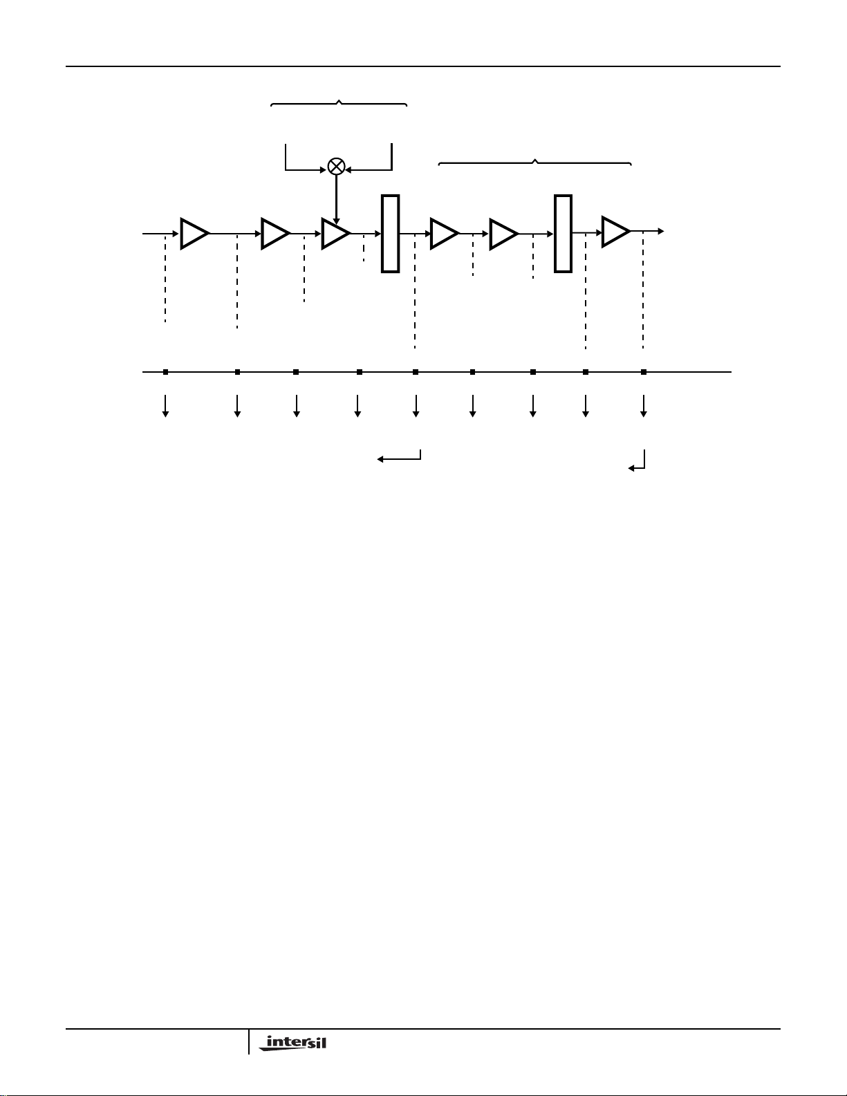
The symbol tracking loop adjusts the baseband sampling
frequency to force sampling of the baseband waveform at
optimal points for data decisions. The ke y elements of this
loop are the Sampling Error Detector and Symbol Tracking
Loop Filter shown in Figure 11. The output of these two blocks
is a frequency correction term which is used to adjust the
baseband sample frequency external to the HSP50210. In
typical applications, the frequency correction term is fed back
to the HSP50110 to adjust baseband sampling via the
Resampling NCO (see HSP50110 Datasheet).
3-266
Page 15
3-267
REGISTER ENABLE RATE
! = SYMBOL RATE
BLANK = CLK RATE
SYMBOL TRACK
LOOP FILTER
LEAD GAIN
FRZ_ST
END
MID
!
MID AND END
Q
SYMBOL SAMPLES
END
Q
MID
R
E
G
SAMPLING ERROR DETECTOR
I
I
DAT A
DECISION
MID-SYMBOL
DAT A
DECISION
MID-SYMBOL
TRANSITION
DETECT
TRANSITION
MID-POINT
TRANSITION
DETECT
TRANSITION
MID-POINT
LEAD
MANTISSA
ACQ
MANTISSA
TRACK
‘0’ ‘-1’‘1’
MUX
ZERO
LEAD
“0”
REG REG
MUX
-
+
“0”
‘0’ ‘-1’‘1’
‘0’
MUX
SINGLE/
DOUBLE
RAIL
SAMPLING
MUX
-
+
+
MUX
ERROR
INVERT
INVERT
ERROR
!
ERROR
ACCUM.
“0”
ZERO
LAG
REG REG
LAG
MANTISSA
ACQ
MUX MUX
MUX
LAG
MANTISSA
TRACK
EXPONENT
LEAD
EXPONENT
LEAD
ACQ
REG
REG
MUX
SHIFT SHIFT
MUX
REG REG
LAG
LAG
ACQ
EXPONENT
TRACK
LEAD
EXPONENT
TRACK
+
MUX
LOAD
ACC
ACCUMULATOR
REG
LIMIT
ACC LIMITS
UPPER/LOWER
LAG
+
SERIAL
OUTPUT
FORMATTER
SOFSYNC
REG
TO
µP
INTERFACE
SOF
HSP50210
FIGURE 11. SYMBOL TRACKING
LAG GAIN
Page 16

HSP50210
Sampling Error Detector
The Sampling Error Detector is a decision based error
detector which determines sampling errors on both the I and
Q processing paths. The detector assumes that it is fed with
samples of the baseband waveform taken in the middle of
the symbol period (mid-symbol sample) and between
symbols (end-symbol sample) as shown in Figure 12. The
sampling error is a measure of how far the mid-symbol
sample is from the symbol transition mid-point. The
transition mid-point is half way between two symbol
decisions. The detector makes symbol decisions by
comparing the end-symbol samples against a selectable
threshold set (see Modulation Order Select bits 9-10 in Table
28). The error term is generated by subtracting the midsymbol sample from the transition mid-point. The sign of the
error term is negated for negatively sloped symbol
transitions. If no symbol transitions are detected the error
detector output is zeroed. Errors on both the I and Q
processing paths are summed and divided by two if Double
Rail error detection is selected (see Symbol Tracking
Configuration Control Register, bit 8: Table 28).
The sampling Error Detector provides an error accumulator
to compensate for the processing rate of the loop filter. The
error detector generates outputs at the symbol rate, but the
loop filter can only accept inputs every eight f
Thus, if the symbol rate is faster than 1/8 CLK, the error
accumulator should be used to accumulate the error until the
loop filter is ready for a new input. If the error accumulator is
not used when the symbol rate exceeds 1/8 CLK, some error
outputs will be missed. For example, if f
CLK
error accumulation is required for symbol rates greater than
5 MSPS (f
CLK
/8).
Note: The loop filter lead gain term
must be scaled accordingly if the accumulator is used.
MID-SYMBOL
SAMPLE
X
X
SAMPLING
ERROR
FIGURE 12. TRACKING ERROR ASSOCIATED WITH BASE-
BAND SAMPLING ON EITHER I OR Q RAIL
(BPSK/QPSK)
X
X
TRANSITION
X
X
MIDPOINT
clocks.
CLK
= 40MHz, then
END-SYMBOL
SAMPLE
EXPECTED
SYMBOL
LEVELS
Output Section). In basic configurations, the SOF output of
the HSP50210 is connected to the SOF input of the
HSP50110.
Two sets of registers are provided to store the loop gain
parameters associated with acquisition and tracking. The
appropriate loop gain parameters are selected manually via
the Microprocessor Interface or automatically via the Carrier
Lock Detector. The loop filter’s lead and lag gain terms are
represented as a mantissa and exponent. The mantissa is a
4-bit value which weights the loop filter input from 1.0 to
1.9375. The exponent defines a shift factor that provides
-1
additional weighting from 2
mantissa and exponent provide a gain range between 2
-32
to 2
. Together the loop gain
-32
and ~1.0 as given by,
Lead/Lag Gain = (1.0+M*2-4)*2
-(32 -E)
(EQ. 10)
where M = a 4-bit binary number from 0 to 15, and E is a 5-bit
binary value ranging from 0 to 31. For example , if M = 0101
and E = 00110, the Gain = 1.3125*2
-26
. They are stored in the
Control Registers described in Table 31 and Table 32.
A limiter is provided on the lag accumulator output to keep the
baseband sample rate within a user defined range (see Table
29 and Table 30). If the lag accumulator exceeds either the
upper or lower limit, the accumulator is loaded with the limit.
For additional loop filter control, the loop filter output can be
frozen by asserting the FZ_ST pin which null the sampling
error term into the loop filter. The lag accumulator can be
initialized to a particular value and can be read via the
microprocessor interface as described in the Section
“Reading from the Microprocessor Interface”, and Table 33.
The symbol tracking loop filter bit weighting is identical to the
carrier tracking loop bit weighting, shown in Figures 9 and 10.
Soft Decision Slicer
The Soft Decision Slicer encodes the I/Q end-symbol
samples into 3-bit soft decisions. The input to the slicer is
assumed to be a bi-polar (2ary) baseband signal
representing encoded values of either ‘1’ or ‘0’. The most
significant bit of the 3-bit soft decision represents a hard
decision with respect to the mid-point between the expected
symbol values. The 2 LSBs represent a level of confidence
in the decision. They are determined by comparing the
magnitude of the slicer input to multiples (1x, 2x, and 3x) of a
programmable soft decision threshold (see Figure 13).
Symbol Tracking Loop Filter
The Symbol Tracking Loop Filter is a second order lead/lag
filter. The sampling error is weighted b y the lag gain and
accumulated to give the integral response (see Figure 11).
The Lag Accumulator output is summed with the sampling
error weighted by the Lead Gain. The result is a frequency
term which is output serially, via the SOF output, to the
NCO/VCO controlling the baseband sample rate (see Serial
3-268
Page 17

HSP50210
HARD DECISION
THRESHOLD
0.0
MSB-1
MSB-1
MSB-1
MSB-1
‘0’ DECISION
‘0’‘1’
0.5
THRESHOLD
2x THRESHOLD
3x THRESHOLD
STRONGERWEAKER
PROBABILITY
DENSITY
FUNCTION
THRESHOLD
THRESHOLD
‘1’ DECISION
STRONGER WEAKER
-0.5
THRESHOLD
2x THRESHOLD
3x THRESHOLD
FS
1/2
MSB
1/3
0
1/3
MSB
1/2
-FS
FIGURE 13. OVERLAY OF THE HARD/SOFT DECISION
THRESHOLDS ON THE SYMBOL PROBABILITY
DENSITY FUNCTIONS (PDFs) FOR BPSK/QPSK
SIGNALS)
The soft decision threshold represents a range of
magnitude values from 0.0 to
to the slicer has a range of 0.0 to
~0.5.
Note: Since the input
~
1.0, the threshold
setting should be set to less than 1.0/3 = 0.33. This
avoidssaturation.
The slicer decisions are output in either
a two’s complement or sign/magnitude format (see Soft
Decision Slicer Configuration Control Register, bit 7: Table
40). The slicer input to output mapping for a range of input
magnitudes is given in Table 7. For example, a negative
input to the slicer whose magnitude is greater than twice
the programmable threshold but less than 3x the threshold
would produce a sign/magnitude output of 110 (BINARY).
The I and Q inputs to the slicer are encoded into 3-bit soft
decisions ISOFT(2-0) and QSOFT(3-0). These signals are
routed to the OUTA(9-4) outputs by the Output
Configuration Control Register Selector bits 0-3 (see
Table 42).
TABLE 7. SLICER INPUT TO OUTPUT MAPPING
SLICER INPUT MAGNITUDE
RELATIVE TO
SIGNAL
INPUT POLARITY
+>>>011011
+>>≤ 010 010
+>≤ < 001 001
+ ≤ < < 000 000
- ≤ < < 100 111
->≤ < 101 110
->>≤ 110 101
- > > > 111 100
1x
THRESHOLD2xTHRESHOLD3xTHRESHOLD
SIGN/MAGNITUDE
OUTPUT
TWO’S
COMPLEMENT
Carrier Phase Error Detector
The Carrier Phase Error is computed by removing the
phase modulation from the phase output of the Cartesian
to Polar Converter. To remove the modulation, the phase
term is rotated and multiplied (modulo 2π) to fold the Phase
Error into an arc centered about 0
whole plane, as shown in Figure 14. The phase rotation is
performed by adding a 4-bit two’scomplement phase offset
(resolution 22.5
o
) to the 4 MSBs of the 8-bit phase term.
The multiplication is performed by left shifting the result
from 0-3 positions with the MSB’s discarded and zeros
inserted into the LSB’s. For example, Carrier Phase Error
produces I/Q constellation points which are rotated from
the expected constellation points as shown in Figure 14. By
adding an offset of 45
o
(0010 0000 binary) and multiplying
by 4 (left shift by two positions) the phase modulation is
removed, and the error is folded into a 90
o
0
. The left axis represents a decision boundary of ±45oC,
implying the vertical axis is ±22.5
The phase offset and shift factors required for different PSK
orders is given in Table 8. Configuration of the Carrier
Phase Error Detector is done via the Carrier Phase Error
Detector Control Register, bits 0-5, (see Table 17). The
Phase Error term may be selected for output via the Output
Selector Configuration Control Register, bits 0-3 (see
Table 42).
o
but encompasses the
o
arc centered at
o
as shown in Figure 14.
OUTPUT
3-269
Page 18

HSP50210
In applications where Phase Error terms are generated
faster than the processing rate of the Carrier Loop Filter, an
error accumulator is provided to accumulate errors until the
loop filter is ready for a new input. Phase Error terms are
generated at the rate I/Q samples are input to the Cartesian
to Polar Converter. However, the Carrier Loop Filter can not
accept new input faster than CLK/6 since six CLK(f
CLK
)
clock edges are required to complete its processing cycle. If
the error accumulator is not used and the I/Q sample rate
exceeds CLK/6, error terms will be missed.
NOTE: The carrier Phase Error terms input to the loop filter are
only generated from the end-symbol samples when the output
of the I&D filter is selected for input to the Cartesian-to-Polar
converter.
NOTE: The loop filter lead gain term must be scaled accordingly
if the accumulator is used.
o
90
45
o
I
X
o
0
o
Q
X
XX
o
-90
DECISION
REGION
BOUNDARY
±45
SHIFT
FACTOR
θ
E
CONSTELLATION
BOUNDARY
ACTUAL
POINT
INPUT TO CARTESIAN/POLAR CONVERTER
DECISION
REGION
o
±180
XX
θ
E
PHASE ROTATION BY 45
PROJECTION OF PHASE ERROR (
FIGURE 14. PHASE ERROR DETECTOR OPERATION (QPSK)
TABLE 8. BASIC PHASE ERROR DETECTOR SETTINGS
MODULA TION
TYPE
CW 0o (00 HEX) 0 (no shift) ±180
BPSK 0o (00 HEX) 1 (left shift 1) ±90
QPSK 45o (20 HEX) 2 (left shift 2) ±45
8-PSK 22.5o(10 HEX) 3 (left shift 3) ±22
90
-90
±180
o
Q
X
X
o
PHASE
OFFSET
o
EXPECTED
CONSTELLATION
POINT
I
o
0
DECISION
REGION
BOUNDARY
o
22.5
Q
o
MULTIPLICATION BY 4
(MODULO 2
θE) ABOUT 0
o
-22.5
o
PHASE ER-
RANGE
X
π)
ROR
θ
E
o
0
I
Carrier Loop Filter
The Carrier Loop Filter is second order lead/lag filter as
shown in Figure 14. The loop filter is similar to the Symbol
Tracking Loop Filter except for the additional terms from the
AFC Loop Filter and the Frequency Sweep Block. The
output of the Lag Accumulator is summed with the weighted
Phase Error term on the lead path to produce a frequency
control term. The Carrier Loop Filter is configured for
operation by the Control Registers described in Tables 20
to 27.
The Carrier Tracking Loop is closed by using the loop filter
output to control the NCO or VCO used to down convert the
channel of interest. In basic configurations, the frequency
correction term controls the Synthesizer NCO in the
HSP50110 Digital Quadrature Tuner via the COF and
COFSYNC pins of the HSP50210’s serial interface (see
Serial Output Section). In applications where the carrier
tracking is performed using the NCO on board the
HSP50210, the loop filter output is fed to the on-board NCO
as a frequency control.
The gain for the lead and lag paths of the Carrier Loop Filter
are set through a programmable mantissa and exponent.
The mantissa is a 4-bit value which weights the loop filter
input from 1.0 to 1.9375. The exponent defines a shift factor
-1
that provides additional weighting from 2
to 2
-32
. Together
the loop gain mantissa and exponent provide a gain range
between 2
Lead/Lag Gain = (1.0+M*2-4)*2
-32
and ~1.0 as given by,
-(32 -E)
(EQ. 11)
where M = a 4-bit binary number from 0 to 15, and E is
a 5-bit binary value ranging from 0 to 31. For example, if
M = 0101 and E = 00110, the Gain = 1.3125*2
-26
. The loop
gain mantissa and exponent are set in the Carrier Loop Gain
Control Registers (see Tables 24 - 25).
The Phase Error input to the Carrier Loop Filter is an 8-bit
fractional two’s complement number between ~1.0 to -1.0
(Format -2
0
. 2-12-22-32-42-52-62-7). Some LSB’s are zero
for BPSK, QPSK and 8-PSK. If minimum loop gain is used,
the Phase Error is shifted in significance by 2
-32
. With
maximum loop gain, the Phase Error is passed almost
unattenuated. The output of the Carrier Loop filter is a 40-bit
fractional two’s complement number between ~1.0 and -1.0
(Format -2
0
. 2-12-22-3..... 2
-392-40
). In typical applications,
the 32 MSBs of the loop filter output represent the
frequency control word needed to adjust the down
converting NCO for phase lock. Tables 9 and 10 illustrate
the bit weighting of the Carrier Loop Filter into the NCO for
both tracking and acquisition sweep modes.
A limiter is provided on the Carrier lag accumulator output to
keep frequency tracking within a user defined range (see
Tables 22 - 23). If the lag accumulator exceeds either the
upper or lower limit the accumulator is loaded with the limit.
For additional loop filter control, the Carrier Loop Filter
output can be frozen by asserting the FZ_CT pin which nulls
the Phase Error term into the loop filter. Also, the lag
accumulator can be initialized to a particular value via the
Microprocessor Interface as described in Table 27 and can
be read via the microprocessor interface as described in
“Reading from the Microprocessor Interface Section”.
3-270
Page 19

3-271
FRZ_CT
TO POLAR
CONVERTER
PHASE OUTPUT
FROM CARTESIAN
DETECT
TO LOCK
TO OUTPUT
SELECT BLOCK
REG
CARRIER PHASE
ERROR DETECT
PHASE
OFFSET
+
SHIFT
REG
PHASE ERROR
(
θ
)
E
DELAY
(1, 2, 4, 8, 16)
-
+
DISCRIMINATOR
SHIFT LEFT
0, 1, 2, 3
“0”
@ OR
*
MUX
ERROR
INVERT
PHASE
ERROR
REGISTER ENABLE RATE
@ = SYNC RATE
CARRIER
LOOP FILTER
MANTISSA
ZERO
LEAD
“0”
@ OR !
INVERT
ERROR
ACCUM.
MUXMUX
“0”
ZERO
LAG
MANTISSA
CARRIER LEAD GAIN
LEAD
LEAD
MANTISSA
ACQ
TRACK
MUX
MUX
LAG
LAG
MANTISSA
ACQ
TRACK
CARRIER LAG GAIN
LEAD
EXPONENT
ACQ
LAG
EXPONENT
ACQ
LEAD
EXPONENT
TRACK
MUX
SHIFT SHIFT
MUX
LAG
EXPONENT
TRACK
+
+
MUX
LOAD
ACC
FROM
MICROPROCESSOR
INTERFACE
UPPER/LOWER
ACCUMULATOR
REG
LIMIT
ACC LIMITS
LAG
LEAD/LEAD + LAG
MUX
+
MUX
LAG/LEAD + LAG
= TWICE SYMBOL
*
! = SYMBOL RATE
BLANK = CLK RATE
REG
REG
SERIAL
OUTPUT
FORMATTER
REG
TO
µP
INTERFACE
TO NCO
COF
COFSYNC
HSP50210
ERROR
FREQUENCY
+
FREQUENCY
SHIFT
SHIFT LEFT
0, 1, 2, 3
SHIFT
REG
CARRIER
FREQUENCY
ERROR DETECT
“0”
AFC LOOP FILTER
ERROR
ACCUM.
“0”
ZERO
AFC
MANTISSA
MUX
ACQ
MUX
MANTISSA
TRACK
EXPONENT
ACQ
AFC GAIN
SHIFT
MUX
EXPONENT
TRACK
MUX
FREQUENCY
ERROR
INVERT
INVERT
ERROR
@ OR !
FIGURE 15. CARRIER ACQUISITION/TRACKING LOOP BLOCK DIAGRAM
FREQUENCY SWEEP
SHIFT
MUX
SWEEP RATE
MANTISSA
ACQ
“0”
TRACK
SWEEP RATE
EXPONENT
ZERO
SWEEP
Page 20

HSP50210
TABLE 9. BIT WEIGHTING IN THE CARRIER LOOP FILTER TO THE NCO - TRACKING
φe
BIT
WEIGHT
40 0f
39 Obtained with a shift of 31 and a Gain of 01.1111 (~2) → (8) - shift31 1 f
38 7. - shift31 2 f
37 6 - shift30 3 f
36 5 - shift29 4 f
35 4 - shift28 5 f
34 3 - shift27 6 f
33 2 - shift26 7 f
32 1 - shift25 8 f
31 0 - shift24 9 f
30 - shift23 10 f
29 - shift22 11 f
28 - shift21 12 f
27 - shift20 13 f
26 - shift19 14 f
25 - shift18 15 f
24 - shift17 16 f
23 - shift16 17 f
22 - shift15 18 f
21 - shift14 19 f
20 - shift13 20 f
19 - shift12 21 f
18 - shift11 22 f
17 - shift10 23 f
16 - shift9 24 f
15 - shift8 25 f
14 - shift7 26 f
13 17 - shift6 27 f
12 (12) 16 17 = (12) (12) - shift5 28 f
11 (11) 15 16 = (11) (11) - shift4 29 f
10 (10) 14 15 = (10) (10) - shift3 30 f
9 (9) 13 14 = (9) (9) - shift2 31 f
8 (8) 0 12 13 = (8) (8) - shift1 32 f
7 7. 1. 11. 12. = 7. 7. - shift0 33 f
6 6 x 10 11 = 6 6 34 f
5 5 x 9 10 = 5 5 35 f
4 4 x 8 9 = 4 4 36 f
3 3 x 7 8 = 3 3 37 f
2 2 6 7 = 2 2 38 f
1 1 5 6 = 1 1 39 f
0 0 4 5 = 0 0 40 f
(AND
ACCOM.)
MANTISSA
GAIN
MULT
OUT
3 (RND)
2
1
0
BITS
KEPT
(RND) SHIFT = 0 SHIFT ≅ 32
SHIFT
COUNTS
NCO BIT
WEIGHT
OUTPUT
FREQUENCY
RESOLUTION
CLK
/2
CLK
/4
CLK
/8
CLK
/16
CLK
/32
CLK
/64
CLK
/128
CLK
/256
CLK
/512
CLK
/1024
CLK
/2048
CLK
/4096
CLK
/8192
CLK
14
/2
CLK
15
/2
CLK
16
/2
CLK
17
/2
CLK
18
/2
CLK
19
/2
CLK
10
/2
CLK
21
/2
CLK
22
/2
CLK
23
/2
CLK
24
/2
CLK
25
/2
CLK
26
/2
CLK
27
/2
CLK
28
/2
CLK
29
/2
CLK
30
/2
CLK
31
/2
CLK
32
/2
CLK
34
/2
CLK
34
/2
CLK
35
/2
CLK
36
/2
CLK
37
/2
CLK
38
/2
CLK
39
/2
CLK
40
/2
CLK
3-272
Page 21

HSP50210
TABLE 10. BIT WEIGHTING IN THE CARRIER LOOP FILTER TO THE NCO - SWEEP
OUTPUT
BIT
WEIGHT φe
40 0f
39 Shift 27 and Gain = 01.1111 → (8) - shift28 1 f
38 7. - shift27 2 f
37 6 - shift26 3 f
36 5 - shift25 4 f
35 4 - shift24 5 f
34 3 - shift23 6 f
33 2 - shift22 7 f
32 1 - shift21 8 f
31 0 - shift20 9 f
30 - shift19 10 f
29 - shift18 11 f
28 - shift17 12 f
27 - shift16 13 f
26 - shift15 14 f
25 - shift14 15 f
24 - shift13 16 f
23 - shift12 17 f
22 - shift11 18 f
21 - shift10 19 f
20 - shift9 20 f
19 - shift8 21 f
18 - shift7 22 f
17 - shift6 23 f
16 - shift5 24 f
15 - shift4 25 f
14 - shift3 26 f
13 - shift2 27 f
12 (12) 0 5 - shift1 28 f
11 (11) 1. 4. - shift0 29 f
10 (10) x 3 30 f
9 (9) x 2 31 f
8 (8) x 1 32 f
77. x 0 33 f
66 z 34 f
55 z 35 f
44 z 36 f
33 z 37 f
22 z 38 f
11 z 39 f
00 z 40 f
NOTE:
min
= 2
-29
at 1% FLB, 4M
5. SW
SWEEP
MANTISSA GAIN SHIFT = 0 SHIFT = 32 SHIFT COUNTS NCO BIT WEIGHT
, 0.075Hz/Baud = 12Kbps.
clk
FREQUENCY
RESOLUTION
CLK
/2
CLK
/4
CLK
/8
CLK
/16
CLK
/32
CLK
/64
CLK
/128
CLK
/256
CLK
/512
CLK
/1024
CLK
/2048
CLK
/4096
CLK
/8192
CLK
14
/2
CLK
15
/2
CLK
16
/2
CLK
17
/2
CLK
18
/2
CLK
19
/2
CLK
10
/2
CLK
21
/2
CLK
22
/2
CLK
23
/2
CLK
24
/2
CLK
25
/2
CLK
26
/2
CLK
27
/2
CLK
28
/2
CLK
29
/2
CLK
30
/2
CLK
31
/2
CLK
32
/2
CLK
34
/2
CLK
34
/2
CLK
35
/2
CLK
36
/2
CLK
37
/2
CLK
38
/2
CLK
39
/2
CLK
40
/2
CLK
3-273
Page 22

HSP50210
Frequency Sweep Block
The Frequency Sweep Bloc k is used during carrier acquisition
to sweep the range of carrier uncertainty. The Sweep Block is
loaded with a programmable value which is input to the lag path
of the Carrier Tracking Loop Filter when frequency sw eep is
enabled.The sweep value is accumulated by the loop filter’slag
accumulator which causes a frequency sweep between the
accumulator’s upper and lo wer limits . When one of the limits is
reached, the sweep value is in v erted to sweep the frequency
back toward the other limit. The F requency Sw eep Bloc k is
controlled by the Lock Detector and is only enabled during
carrier acquisition (see Lock Detector Control Section).
A stepped acquisition mode is provided for microprocessor
controlled acquisition. In the stepped acquisition mode, the lag
accumulator is incremented or decremented by the
programmed sweep v alue each time the loc k detector is
restarted during acquisition. This technique prevents the loop
from sweeping past the lock point bef ore the microprocessor
can respond. Typically in stepped acquisition mode, the step
value is set to a percentage of the loop bandwidth. A dwell
counter is also provided for stepped acquisition. This counter
holds off the lock detector integration from 1 to 129 symbols to
allow the loop to settle before starting the integration.
The sweep value is set via a prog rammab le mantissa and
exponent. The format is 01.MMMM * 2
MMMM is the 4-bit mantissa and EEEEE is the 5-bit exponent
and the weighting is relative to the MSB of the NCO control
word.In swept acquisition mode,the sweep value is the amount
that the carrier lag accumulator is incremented or decremented
each time a new filter output is calculated (sweep rate/N). In
stepped acquisition mode, it is the amount the lag accumulator
is incremented or decremented each time that the lock detector
is restarted. (See Frequency Sweep/AFC Control Loop Control
Register, Table 26.)
-(28 - EEEEE)
where
Carrier Frequency Detector
The Frequency Detector generates a frequency term for use
in Automatic F requency Control (AFC) configur ations . The
Frequency Detector (discriminator) subtracts a previous
Phase Error sample from the current one (d/dt) to produce a
term proportional to the carrier frequency. The discriminator
gain is adjusted by programming a variable delay (1-16)
between the samples subtracted (see Frequency Detector
Control Register; Table 18).
NOTE: The inputto the discriminator corresponds to phase terms
taken from baseband samples at either the SYNC rate or twice
symbol rate depending on the input source chosen for the Cartesian to Polar converter.
Carrier Frequency Error Detector
The Frequency Error Detector is used to generate a frequency
error term for FSK modulated wave f orms. The error is
computed by adding an offset and shifting the frequency
detector output in a manner similar to that used by the Phase
Error Detector. F or PSK demodulation, this b loc k is b ypassed
by setting the offset and shift terms to zero (see Frequency
Error Detector Control Register; Table 19). The frequency error
term may be selected for output via the Output Select Block.
(See Serial Output Configuration Control Register, Table 42).
Automatic Frequency Control (AFC)
Loop Filter
The AFC Loop Filter supplies a frequency correction term to
the lag path of the Carrier Loop filter. The frequency
correction term is generated by weighting the output of the
Frequency Error Detector by a user progr ammable weight
(see Sweep/AFC Control Register; Table 26).
Note: If AFC is
not desired, the frequency error term to the loop filter is
nulled via the Carrier Tracking Configuration Control
Register #2 (see T ab le 21).
Serial Output Interfaces
Frequency control data for Carrier and Symbol Tracking is
output from the DCL through two separate serial interfaces.
The Carrier Offset frequency control is output via the COF
and COFSYNC pins. The Symbol Tracking Offset frequency
control is output via the SOF and SOFSYNC pins. A
SLOCLK is provided to allow for reduced serial rate data
exchanges.The timing relationship of these signals is shown
in Figure 16.
CLK
COFSYNC/
SOFSYNC
COF/
SOF
NOTE: Data must be loaded MSB first.
FIGURE 16. SERIAL OUTPUT TIMING FOR COF AND SOF
OUTPUTS
Each serial word has a programmable word width of either 8,
12, 16, 20, 24, 28, 32, or 40 bits (see Table 41, CW27, bits
4-6 for COF and bits 0-2 for SOF). The polarity of the sync
signals is programmable and is set in CW27 bit 12 for SOF
and bit 11 for COF. The polarity of the serial clock to the
serial data is programmed via CW27 bit 10. If reduced rate
frequency updates is required, the SLOCLK rate is selected
via CW27 bit 7 and the rate is set via CW27 bits 8-9, to be
either CLK/2, CLK/4, CLK/8 or CLK/16. Note that if the DCL
is used with the HSP50110 DQT, then the SLOCLK cannot
be used, i.e. the serial clock must be set to be CLK.
MSB
LSB
MSB
Lock Detector
The Lock Detector consists of the Dwell Counter, Integration
Counter, Phase Error Accumulator, False Lock/Frequency
Accumulator, Gain Error Accumulator and the Lock Detect
State Machine (see Figure 16). The function of the Lock
Detector is to monitor the baseband symbols and to decide
whether the Carrier Tracking Loop is locked to the input
3-274
Page 23

HSP50210
signal.
Note: The Symbol Tracking Loop locks
independently; under most circumstances, it will lock
before the Carrier Tracking Loop locks up.
in-lock/out-of-lockdecision, either the Acquisition or Tracking
parameters are selected in the Carrier Tracking Loop, the
Symbol Tracking Loop and in the Lock Detector itself. The
Lock Detector can be configured either to make the “lock”
decision automatically using the State Machine Control
Mode, or to collect the necessary data so that an external
microprocessor can control the acquisition/tracking process
via the Microprocessor Control Mode (see Figure 22).
In State Machine Control Mode, the Lock Detector State
Machine monitors the outputs of the Phase Error Accumulator
and the False Lock Accum ulator to determine the Lock
Detector state. Accumulation effectiv ely a v erages the Phase
Error and false lock count, reducing their variance. Loc k is
detected by accumulating the magnitude of the Phase Error
over a predetermined interval up to 1025 symbols (the
Integration Time). When the Carrier Loop is locked, the
Integration Period will end bef ore an o v erflo w occurs in the
Phase Error Accumulator. At the beginning of a loc k detection
cycle,the Phase ErrorAccumulator and the Integration Counter
are loaded with their respective pre-load values. With each end
bitsample, the Phase Error Accumulator adds the magnitudeof
the current Phase Error to its accumulated sum, while the
Integration Counter decrements one count. The Lock Detector
State Machine monitors the overflow bit of the Phase Error
Accumulator and the output of the Integration Counter . If the
Phase Error Accumulator overflows bef ore the Integ ration
Counter reaches zero,then the accumulated Phase Error is too
large for the Carrier Tracking Loop to be in lock and the Lock
Detector State Machine goes into the Search state (see Lock
Detector State Machine below). In the search state, the loop
parameters are reloaded with “Acquisition” rather than
“Tracking” values. When the Phase Accumulator overflows or
when the Integration Counter reaches zero, the Integ ration
Counterand the accumulators are re-initialized and the process
begins again. The Integration Counter Pre-load corresponds to
the number of symbols over which to integrate . The Phase
Error Preload corresponds to the distance the Phase Error
Accumulator starts away from overflo w. This distance divided
by the Integration P eriod equals the a v erage Phase Error. The
pre-load value is calculated using:
Preload =
Lock Threshold
Full Scale
----------------------------------------------
–
Full Scale Phase
x 128 x Integration Count
where
18
Full scale = 2
Full scale phase = 180
-1
o
for CW, 90o for BPSK, 45o for QPSK,
etc;
Lock Threshold <45o for BPSK, <22.5o for QPSK, etc.
(typical after shift); and Integration Count = Integration
Period measured in symbol times.
Based on the
(EQ. 12)
The False Lock Detector is used to indicate false lock on
square wave data in a high SNR environment. A false lock
condition is detected bymonitoring the final integration stage
in the Q branch of the Integrate and Dump Filter (see Figure
3). If the magnitude of the integration over the symbol period
is less than the integration over half a symbol period, a
possible false lock condition is detected; (integration over a
symbol period has gone from end-bit to end-bit, while
integration over half the symbol period has gone from the
previous end-bit to mid-bit). By accumulating the number of
these occurrences over the Integration Period, the Lock
Detector State Machine determines whether a false lock
condition exists. The False Lock Accumulator is used to
accumulate the number of possible false lock occurrences
overthe Integration Period. The False Lock Accumulator can
also be configured to accumulate the output of the
FrequencyError Detector (see Lock Detection Configuration
Control Register bit 27: Table 34).
The Gain Error Accumulator provides a mechanism to
estimate data quality (E
). The accumulator integrates
s/No
the magnitude of the gain error of the end-bit samples, over
the Integration Period.
Note: The Gain Error end-bit data
is valid only after lock has been declared, and the
demod is the tracking mode.
The accumulated value
gives an indication of the variance about the ideal
constellation points. The accumulator output is read via the
Microprocessor Interface. The Gain Error Accumulator is
always pre-loaded with zero.
For applications where stepped acquisition is used, a Dwell
Counter is provided. In this mode, the lag accumulator in the
Carrier Loop Filter is stepped to a new frequency after each
Lock Detector integration. The Dwell Counter is used to hold
off Lock Accumulator integration until the loop has a chance
to settle.
Lock Detector Control
The selection of acquisition and tracking modes is controlled
by either the internal state machine or an external
microprocessor. The internal state machine monitors the
rollover of the Phase Error Accumulator and the False Lock
Accumulator relative to the Integration Counter. Depending
on whether the accumulators or counter roll over first, the
acquisition or tracking parameters are selected for the Loop
Filters and the Lock Detector Accumulators. In addition, the
state machine controls the frequency sweep input to the
Carrier Tracking Loop.
The flow of the acquisition control is shown in the State
Diagram in Figure 17. The state machine controls the
acquisition process as described below:
Search. The frequency uncertainty is swept by enabling the
Frequency Sweep Block to the lag path of the Carrier
Tracking Loop Filter. The acquisition parameters are enabled
to the Loop Filters and the Lock Detector Accumulators.
Phase lock is obtained when the Lock Counter rolls over
before the Phase Error Accumulator (average Phase Error is
less than the lock threshold).
3-275
Page 24

HSP50210
Verify. Once phase lock is obtained, the frequency sweep is
disabled and the tracking parameters are enabled. Lock is
verified if the accumulated Phase Error is below the
threshold for a programmablenumber of Integration Periods.
False lock conditions are also monitored by comparing the
roll over of the False Lock Accumulator to that of the
Integration Counter. If the False Lock Accumulator rolls over
before the Integration Counter, a false lock condition exists.
False Lock. Once a false lock has been determined, the
Frequency Sweep block is enabled to move the carrier
tracking beyond the false lock region. The Frequency Sweep
is performed for a programmable number of Integration
Periods before returning to the search state.
Lock. When phase lock has been verified, the Lock status
output is asserted and the False Lock Detector is disabled.
The lock state is maintained as long as the Integration
Counter rolls over before the Phase Error Accumulator.
If the acquisition and tracking process is controlled externally,
the Phase Error Accumulator and False Loc k Accum ulators
DWELL
COUNT
ACQ
“0”
TRACK
INT
PERIOD
ACQ
MUXMUX
INT
PERIOD
TRACK
PHASE
ERROR
PRELOAD
ACQ
PHASE
ERROR
PRELOAD
TRACK
MUX
PHASE
ERROR
|X|
are monitored by an external processor to determine when
lock has been achieved. In this mode the accum ulator preloads are typically set to zero and the accumulator output is
compared in the processor against a threshold equal to the
maximum Phase Error per sample times the number of
samples per Integration Period. The accumulators stop after
each Integration Period to hold their outputs for reading via
the Microprocessor Interface(see Read Enable Address Map;
Table 11). The accumulators are restarted by writing the
Initialize Lock Detector Control address (see Initialize Lock
Detector Control Register: Tab le44). Tosimplify the processor
interface, the LKINT output is provided to interrupt the
processor when the accumulator integration period is
complete. The processor controls the use of the
acquisition/tracking parameters and lock status line by setting
the appropriate bits in the Acquisition/Tracking Configuration
Control Register (see Table 37). In addition, the frequency
sweep function is enabled via the Microprocessor Interface.
FALSE
LOCK
PRELOAD
ACQ
FALSE
LOCK
PRELOAD
TRACK
MUX
FALSE LOCK/
FREQUENCY
ERROR
|X|
“0”
GAIN
ERROR
|X|
DWELL
COUNTER
TC START TC
SWEPT
INTEGRATION
COUNTER
MUX
LOCK DETECTOR STATE MACHINE
+
MUX
REG
OVERFLOW OVERFLOW
ACQUIRE/
TRACK
FIGURE 17. LOCK DETECTOR BLOCK DIAGRAM
+
MUX
REG REG
+
3-276
Page 25

PHASE ERROR
ACCUMULATOR
FINISHES BEFORE
INTEGRATION COUNTER
INTEGRATION
COUNTER FINISHES
BEFORE
PHASE ERROR
ACCUMULATOR
LOCK COUNTER
FALSE
DONE
HSP50210
PHASE ERROR ACCUMULATOR
FINISHES BEFORE
INTEGRATION COUNTER
SEARCH
PHASE ERROR
ACCUMULATOR
FINISHES BEFORE
INTEGRATION
COUNTER
INTEGRATION
COUNTER
FINISHES BEFORE
PHASE ERROR
ACCUMULATOR
AND VERIFY
COUNTER DONE
FALSE LOCK
ACCUMULATOR
BEFORE
LOCK COUNTER
FALSE
LOCK
FALSE
LOCK COUNTER
NOT DONE
INTEGRATION COUNTER
FINISHES BEFORE
PHASE ERROR ACCUMULATOR
VERIFYLOCK
INTEGRATION COUNTER
FINISHES BEFORE
PHASE ERROR
ACCUMULATOR AND
VERIFY COUNTER
NOT DONE
FIGURE 18. ACQUISITION/TRACKING STATE DIAGRAM
Serial Output Controller
The frequency correction terms generated by the Symbol
and Carrier Loop Filters are output through two separate
serial interfaces. The symbol frequency offset used to close
the symbol Tracking Loop is output via the SOF and
SOFSYNC outputs. The carrier offset frequency used to
close the Carrier Tracking Loop is output via the COF and
COFSYNC outputs.
The serial output timing, identical for both of the loop filter
outputs, is shown in Figure 18. The data word is output MSB
first starting with the first rising edge of either CLK or
SLOCLK that follows the assertion of sync (COFSYNC or
SOFSYNC). The HSP50210 is configured to output the
serial data with either CLK or SLOCLK (see Serial Output
Configuration Control Registers bit 7, Table 41). The
SLOCLK output is a programmable sub-multiple of CLK
which is provided for applications requiring a slower serial
clock. In applications where the HSP50210 is used with the
HSP50110, both parts must be supplied with the same CLK
and the HSP50210 is configured to use CLK as the serial
clock. The serial output can be configured for word
containing from 8 to 40 bits.
CLK/
SLOCLK
COFSYNC/
SOFSYNC
COF/
SOF
MSB MSB
NOTE: COFSYNC and SOFSYNC shown Configured as active
“High”.
FIGURE 19. SERIAL OUTPUT TIMING FOR COF AND SOF
OUTPUTS
Output Selector
The output selector determines which internal signals are
multiplexed to the AOUT9-0 and BOUT9-0 outputs. Fifteen
differentoutput options are provided: ISOFT(2:0), QSOFT(2:0),
IEND(7:1), QEND(7:1), AGC(7:1), MAG(7:0), Phase(7:0),
FREQERR(7:1), GAINERR(7:1), BITPHERR(7:1),
CARPHERR(7:1), LKACC(6:0), LKCNT(6:0), NCOCOS(9:0),
and STATUS (6:0). These are detailed in the Output Selector
Configuration Control Register, bits 0-3 (see Table 42).
3-277
Page 26

HSP50210
The status bit definition is:
STATUS BIT DEFINITION
6 Carrier Tracking Loop Lock
5 Acq/Trk
4 Frequency Sweep Direction
3 High Power
2 Low Power
1 Data Rdy
To simplify the output interface, a symbol clock (SMBLCLK)
is output which is synchronous to the soft bit decisions
produced by the Slicer. The SMBLCLK is a 50% duty cycle
clock whose rising edge is centered in the middle of the
output data period for both the soft bit decisions and the endsymbol samples, as shown in Figure 19.
SMBLCLK
ISOFT2-0/
QSOFT2-0/
IEND7-1/
QEND7-1
FIGURE 20. OUTPUT DATA CLOCK TIMING
Microprocessor Interface
The Microprocessor Interface is used to write the
HSP50210’s Control Registers and monitor various read
points within the demodulator. Data written to the interface is
loaded into a set of four 8-bit holding registers, one Write
Address Register, or one Read Address Register. These
registers are accessed via the 3-bit address bus (A0-2) and
an 8-bit data bus (C0-7) as shown in Table 11. The R/W
column indicates whether the data is read from or written to
the given address.
TABLE 11. READ/WRITE ADDRESS MAP FOR
MICROPROCESSOR INTERFACE
R/
W A2-0 DESCRIPTION
W 000 Input Holding Register 0. Transfers to bits 7-0 of the
target control register. Bit 0 is the LSB of the target
register.
W 001 Input Holding Register 1. Transfers to bits 15-8 of the
target control register.
W 010 Input Holding Register 2. Transfers to bits 23-16 of a
32-bit target control register.
W 011 Input Holding Register 3. Transfers to bits 31-24 of the
target control register. Bit 31 is the MSB of the 32-bit
register.
W 100 Write Address Register.Theregister is loaded with the
address of the control register targeted for update.
Theaddress map for the control registers is given in
Tables 1C-32C.
NOTE: Addresses outside the range 0-31 are invalid.
TABLE 11. READ/WRITE ADDRESS MAP FOR
MICROPROCESSOR INTERFACE (Continued)
R/
W A2-0 DESCRIPTION
W 101 Read Address Register. The address loaded into this
register specifies an internal read point as given the by
address map in Table 12. Addresses outside the range
0-4 are invalid.
R 000 Selects output holding register bits 7-0 for output on
C7-0 respectively.Bit 0 is the LSB of the internal holding register.
R 001 Selects output holding register bits 15-8 for output on
C7-0, respectively.
R 010 Selects output holding register bits 23-16 for output on
C7-0, respectively.
R 011 Selects output holding register bits 31-24 for output on
C7-0, respectively. Bit 31 is the MSB.
R 100 Multiplexes 8 bits of internal status out on C7-0. See
Table 13 for bit map.
Data is read from an Internal Status Register and a series of
output holding registers. The output holding registers range
in size from 8 to 32 bits, and their contents are multiplexed
out a byte at a time on C7-0 by controlling A2-0 and
asserting
RD. The addresses listed in Table 11 with the R
indicator provide the address map used for reading data
from the Microprocessor Interface.
Writing to the Microprocessor Interface
The HSP50210 is configured for operation by loading a set
of thirty-two control registers which range in size from 0 to
32 bits. They are loaded by first writing the configuration
data to the Microprocessor interface’s four holding registers
and then writing the target address to the Write Address
Register as shown in Figure 19. The Control Register
Address Map and bit definitions are given in Tables 14 - 45.
The configuration data is transferred from the holding
registers to the target control register on the fourth clock
following a write to the address register. As a result, the
holding registers should not be updated any sooner than 4
CLKs after an address register write (see Figure 20).
NOTE: The holding registers which map to the unused bits of a
particular control register do not have to be loaded.
Reading from the MicroprocessorInterface
The Microprocessor Interface is used to monitor
demodulator operation by providing the ability to read the
accumulator contents in the Lock Detector and Loop
Filters. In addition, the interface is used to monitor the
HSP50210’s Internal Status Register. More clearly, the
following data is available to be read:
3-278
Page 27
HSP50210
#
REGISTERS DEFINITION
(4) 32-Bit Carrier Loop Letter Lag Acc. Output
(4) 32-BitSymbol Tracking Loop Letter Lag Acc. Output
(1) 8-Bit AGC Loop Letter Output
(2) 16-Bit Lock Detectorφe Acc. Output
(2) 16-Bit Lock Detector GE Acc. Output
(2) 16-Bit Lock Detector FL/FE Acc. Output
(1) 8-Bit Internal Status
Total = 16
A different read procedure is required depending on
whether the Lock Detector Accumulators, loop filter
accumulators, or the Status Register is to be read. The
read procedures are summarized in Figures 21 - 23.
The accumulators in the AGC Loop Filter, Carrier Loop
Filter and Symbol Tracking Loop can be read via the
Microprocessor Interface. Since these accumulators are
free running, their contents must be loaded into output
holding registers before they can be read. Each
accumulator has its own output holding register. The three
holding registers are updated by loading 29 (decimal) into
the Write Address Register of the Microprocessor Interface.
The output of a particular holding register is then enabled
for reading by loading its address into the Read Address
Register (see Tables 13 and 14). The holding register
addresses for the loop filter accumulators range from 0 to 4
as given in Table 12. The contents of the output holding
registers are multiplexed out a byte at a time on C7-0 by
changing A2-0 and asser ting RD (see Read/Write Address
Map in Table 11).
TABLE 12. READ ENABLE ADDRESS MAP
ADDRESS HOLDING REGISTER ENABLE
0 Carrier Loop Filter Lag Accumulator. Enables output
of holding register containing 32 MSBs of the lag
accumulator.
1 Symbol Tracking Loop Filter Lag Accumulator.
Enables output of holding register containing 32
MSBs of the lag accumulator.
2 AGC GAIN. Enables output of holding register
containing 8 MSBs of the AGC accumulator.
3 Lock Detector 1. The 16 MSBs of the Lock
Detector’s Phase Error Accumulator and the 16
MSB’s of the False Lock Accumulator are enabled
for output. The accumulator contents are selected
for output as follows, A2-0 = 3 (decimal) selects
MSByte of the Phase Error Accumulator, A2-0 = 2
(decimal) selects LSByte of the Phase Error
Accumulator, A2-0 = 1 (decimal) selects MSByte of
the False Lock Accumulator, and A2-0 = 0 (decimal)
selects LSByte of the False Lock Accumulator.
4 Lock Detector 2. Enables the 16 MSBs of the Lock
Detector’s Gain Error Accumulator for output. The
MSByte of the accumulator is selected for output by
setting A2-0 = 1, and the LSByte is selected by
A2-0 = 0.
The contents of the three accumulators in the Lock Detector
can also be read via the Microprocessor Interface. However,
the Lock Detector must be stopped before a read can be
performed. In State Machine Control Mode, the Lock
Detector is stopped by loading 24 (decimal) into the Write
Address Register. In Microprocessor Control Mode, the Lock
Detector stops after each Integration Period. To determine
when the Lock Detector has stopped and is ready for
reading, bits 7 and 6 of the Internal Status Register (SR7&6)
must be monitored (see Table 15). The control sequence for
reading a Lock Detector Accumulator is shown in Figure 22.
The control sequence for reading a Lock Detector
Accumulator using the LKINT signal is shown in Figure 23.
3-279
An 8-bit Internal Status Register (SR7-0) can also be
monitored via the Microprocessor interface. The Status
Register indicates loop filter and Lock Detector status as
listed in Table 13. The Status Register contents are output
on C7-0 by setting A2-0 to 100(binar y) an asserting RD as
shown in Figure 24. The register contents are updated
each CLK.
Page 28

HSP50210
WR
RD
DON’T CARE
A0-2
SIGNALS
PROCESSOR
C0-7
CLK
EARLIEST TIME ANOTHER
NOTE: These processor signals are meant to be representative. The actual shape of the waveforms will be set by the microprocessor used. Verify
that the processor waveforms meet the parameters in the Waveforms Section of this data sheet to ensure proper operation. The Processor waveforms are not required to be synchronous to CLK. They are shown that way to clarify the illustration.
FIGURE 21. CONTROL REGISTER LOADING SEQUENCE
WR
RD
DON’T CARE
A0-2
SIGNALS
PROCESSOR
C0-7
CLK
1234
5 6
3154 02
MSB LSB029
43210 01
1234
LOAD CAN BEGIN
ADDRESS IS ASYNCHRONOUS TO CLK
DATA IS
ASYNCHRONOUS
TO CLK
1 2 3 4 5
LOAD OUTPUT
HOLDING REG
ENABLE
HOLDING
REG
FOR
READ
WAIT
6 CLKs
DELAY
TO
RD
ASSERT
READ READ READ READ
NOTE: These processor signals are meant to be representative. The actual shape of the waveforms will be set by the microprocessor used. Verify
that the processor waveforms meet the parameters in the Waveforms Section of this data sheet to ensure proper operation. The Processor waveforms are not required to be synchronous to CLK. They are shown that way to clarify the illustration.
1
Load the Write Address Register with 29
2
Enable Carrier Loop Filter Lag Accumulator holding register for reading.
3
Select the MSByte of the output holding register for output.
4
Assert RD low to output data on C0-7. (Must wait for 6 CLKs after loading the holding registers).
5
Select other bytes of holding register by changing A0-2 and asserting RD.
to load the output holding registers.
dec
FIGURE 22. LOOP FILTER ACCUMULATOR READ SEQUENCE
3-280
Page 29

HSP50210
WR
RD
A0-2
SIGNALS
PROCESSOR
C0-7
CLK
DCL
SR-7
SIGNALS
3
SR7=0
1 2 3 5 6 8 6 8 6 8
HALT LD
AT END OF
CYCLE
ENABLE
LD REG.
FOR READING
4254 13
SR7=1
STATUS READS
74
PE
MSW
8 6
LOCK DETECTION STATUS READSINTERNAL
PE
LSW
FL
MSW
NOTE: These processor signals are meant to be representative. The actual shape of the waveforms will be set by the microprocessor used. Verify
that the processor waveforms meet the parameters in the Waveforms Section of this data sheet to ensure proper operation. The Processor waveforms are not required to be synchronous to CLK. They are shown that way to clarify the illustration.
1
Load the Write Address Register with 24
tohalt the Lock Detector after the current integration cycle. This disables the reload ofthe integration
dec
counter in the lock detector. The verify counter is not reset and will resume at the stopped value when the lock detector is restarted.
2
Load the Read Address Register with 3
3
Read Internal Status Register to monitor SR-7 to determine when the Lock Detector is stopped and ready to be read.
4
SR-7 goes high, indicating the Lock Detector integration cycle is complete, and ready to be read.
5
Read Internal Status Register and find SR-7 = 1; the Lock Detector is ready to be read.
6
Change Read address to (3; 2; 1; 0) for (Phase Error MSW; PE LSW; False Lock MSW; FL LSW) read.
7
End of Internal Status Valid Data.
8
Assert RD to Read Lock Detector Status
9
Load The Write Address Register with 30
to enable the Lock Detector Phase Error Accumulator for reading.
dec
to initialize Lock Detector Accumulators and Reset the Integration counters. (Not needed for state
dec
machine mode).
10
Load the Write Address Register with 25
to restart the Lock Detector.
dec
FIGURE 23. PROCESSOR MONITORING INTERNAL STATUS/READING LOCK DETECTOR
0
FL
LSW
9
RESET
DETECTOR
3024
LOCK
4
10
RESTART
LOCK
DETECTOR
25
TABLE 13. INTERNAL STATUS REGISTER (SR7-0) BIT MAP
BIT BIT DESCRIPTION
7 Lock Detector Stopped and Ready for Reading
(State Machine Control Mode).
0 = Lock Detector not stopped.
1 = Lock Detector stopped, ready for read.
6 Lock Detector Stopped and Ready for Reading
(Microprocessor Control Mode).
0 = Lock Detector not stopped.
1 = Lock Detector stopped, ready for read.
5 CarrierLoop Filter Lag Accumulator Load Complete. This bit
is used to determine when a 32-bit load of Carrier Lag Accumulator is complete. The accumulator load is initialized by
loading the Write Address Register with 13 (decimal) as described in Table 27.
0 = Load not complete.
1 = Load complete.
4 Symbol Tracking Loop Filter Lag Accumulator Load
Complete. This bit is used to determine when a 32-bit load
of Symbol Track Lag Accumulator is complete. The
accumulator load is initialized by loading the Write Address
Register with 19 (decimal) as described in Table 33.
0 = Load not complete.
1 = Load complete.
BIT BIT DESCRIPTION
3 Lock. Carrier Lock state achieved by Lock Detector.
0 = Not locked.
1 = Locked.
2 Acquisition/Track. Indicates whether the Lock Detector is in
acquisition or tracking mode.
0 = Tracking Mode.
1 = Acquisition Mode.
1 Reserved.
0 Frequency Sweep Direction, defined for upper sideband sig-
nals.
0 = UP.
1 = DOWN.
3-281
Page 30

WR
RD
HSP50210
A0-2
SIGNALS
PROCESSOR
C0-7
CLK
SR-7
DCL
SIGNALS
LKINT
1 2
3
3 4 5 6 5 6 5 7 8 9 10
PE
MSW
2035 41
PE
LSW
FL
MSW
5 6
FL
LSW
4
30
25
NOTE: These processor signals are meant to be representative. The actual shape of the waveforms will be set by the microprocessor used. Verify
that the processor waveforms meet the parameters in the Waveforms Section of this data sheet to ensure proper operation. The Processor waveforms are not required to be synchronous to CLK. They are shown that way to clarify the illustration.
1
LKINT Asserts Indicating End of Lock Detector Accumulation Cycle; Accumulators Ready to Read.
2
Set A0-2 to 5 for Reading Lock Detector.
3
Load Read Address Register with 3
4
Set A0-2 to 3 for Phase Error (PE) Read.
5
Assert RD and read (Phase Error (PE) MSW; PE LSW; False Lock (FL) MSW; FL LSW).
6
Change Read Address to (2; 1; 0) to read various Lock Detection values.
7
Change Address to 4 to Initialize the Lock Detector.
8
Load Write Address Register with 30
to enable the Lock Detector Phase Error Accumulator for Reading
dec
to initialize the Lock Detector Accumulators and Reset Integration Counters. (Only has an effect in µP
dec
mode).
9
Keep Address to 4 to Restart the Lock Detector.
10
Load Write Address Register with 25
to restart the Lock Detector. (Only necessary if not in the µP mode).
dec
FIGURE 24. PROCESSOR INTERRUPT MONITOR/LOCK DETECTOR READ
.
CLK
RD
A0-2
C7-0
STATUS CAN CHANGE EVERY CLK
4
FIGURE 25. INTERNAL STATUS REGISTER READ
3-282
Page 31

HSP50210
TABLE 14. DATA PATH CONFIGURATION CONTROL REGISTER
DESTINATION ADDRESS = 0
BIT
POSITION FUNCTION DESCRIPTION
31-27 Reserved Reserved. Set to 0 for proper operation.
26-24 Integrate/Dump Shifter
Gain
23-16 Input Level Detector
Threshold
15 Input Data Format Select 0 = Two’s Complement Input .
14 Serial/Parallel Input
Select
13 Input Level Detector
Output Select
12 Q Input to Complex
Multiplier
11 I Input to Complex
Multiplier
10 Complex Multiplier
Bypass
9 Demodulation/Loop
Filter Mode
Select
8 Cartesian/Polar Input
Select
7 RRC Filter Enable 0 = Enable RRC filter.
6 Integrate and Dump
Filter Test Mode
5 Integrate and Dump
Input Select
4-1 Integrate and Dump
Decimation Select
0 OQPSK Data
De-Skew Select
These bits set the shifter attenuation in the Integrate/Dump Filter.
000 = No Shift (Gain = 20).
001 = Right Shift 1 (Gain = 2-1).
010 = Right Shift 2 (Gain = 2-2).
011 = Right Shift 3 (Gain = 2-3).
100 = Right Shift 4 (Gain = 2-4).
Other Codes are invalid.
This register sets the magnitude threshold for the Input Level Detector (see Input Level Detector
Section). This 8-bit value is a fractional unsigned number whose format is given by:
20. 2-1 2-2 2-3 2-4 2-5 2-6 2-7.
The possible threshold values range from 0 to 1.9961 (00 - FF hex). The magnitude range for complex
inputs is 0.0 - 1.4142 while that for real inputs is 0.0 - 1.0.
threshold produces a maximum output of 1.375, therefore a threshold of greater than 1.375 will
never be exceeded.
1 = Offset binary Input.
0 = Parallel Input.
1 = Serial Input.
0 = HI/LO output of 1 means input ≤ threshold .
1 = HI/LO output of 1 means input > threshold.
0 = QIN9-0 enabled to Complex Multiplier.
1 = Q input to Complex Multiplier zeroed.
0 = IIN9-0 enabled to Complex Multiplier.
1 = I input to complex multiplier set to negative full scale (200 Hex).
0 = Data enabled to Complex Multiplier (Multiplied by output of NCO).
1 = Complex Multiplier Bypassed.
0 = Error detector outputs routed to Loop Filters (Normal Mode of Operation).
1 = Part functions as dual Loop Filters. The IIN9-0 input is routed to the Symbol Loop Filter; the QIN90input is routed to the Carrier Loop Filter. Dataisgated into the Loop Filters with the assertion of SYNC.
0 = Enable output of AGC Multiplier to Cartesian to Polar Converter.
1 = Enable output of Integrate and Dump Filter to the Cartesian to Polar Converter.
1 = Bypass RRC filter.
0 = End-Symbol Samples routed to Output Formatter.
1 = Both End and Mid Symbol routed to Output Formatter: End-symbol samples occur when
SMBLCLK is high; Mid-Symbol samples occur when SMBLCLK is low.
0 = Input taken from output of Frequency Discriminator (FSK routing).
1 = Input taken from output of AGC Multiplier (Select this setting for PSK demodulation).
Bit 4 is the MSB.
1000 = No Decimation (no accumulation, no sample pair summing).
0000 = Decimation by 2 (no accumulation, sample pair summing).
0001 = Decimation by 4 (accumulate 2 samples, sample pair summing).
0010 = Decimation by 8 (accumulate 4 samples, sample pair summing).
0011 = Decimation by 16 (accumulate 8 samples, sample pair summing).
0100 = Decimation by 32 (accumulate 16 samples, sample pair summing).
All other codes are invalid.
0 = Disables Q channel data delay.
1 = Delays Q Channel by 1/2 Symbol time to remove OQPSK stagger.
Note: The algorithm used to estimate
3-283
Page 32

HSP50210
TABLE 15. POWER DETECT THRESHOLD CONTROL REGISTER
DESTINATION ADDRESS = 1
BIT
POSITION FUNCTION DESCRIPTION
31-8 Not Used No programming required.
7-0 Power Threshold The THRESH output is driven low when the magnitude output of the Cartesian to Polar Converter
exceeds the threshold programmed here. The threshold is represented as an 8-bit fractional unsigned
value with the following format:
20. 2-1 2-2 2-3 2-4 2-5 2-6 2-7.
Using this format, the possible range of threshold values is between 0 to 1.9961. Bit position 7 is the MSB .
TABLE 16. AGC LOOP PARAMETERS CONTROL REGISTER
DESTINATION ADDRESS = 2
BIT
POSITION FUNCTION DESCRIPTION
31 Enable AGC 0 = Gain error enabled to AGC Loop Filter.
1 = Gain error into AGC Loop Filter set to zero.
30-28 AGC Loop Gain
Exponent (E)
27-24 AGC Loop Gain
Mantissa (M)
23-16 AGC Threshold The AGC gain error is generated by subtracting the threshold value programmed here from the
These bits set the loop gain exponent as given by:
AGC Loop Gain Exponent = 2
where EEE corresponds to the 3-bit binary value programmed here. Thus, a gain range from 2-7to 2
may be achieved for EEE = 000 to 111 Binary. Bit position 30 is the MSB. See Table 3.
The loop gain mantissa is represented as a 4-bit unsigned value with the following format:
AGC Loop Gain Mantissa = 0. 2-12-22-32-4; 0.MMMM.
Thisformat provides a mantissa range from 0.0 to 0.9375 formantissasettings from 0000 to 1111 Binary.
Bit position 27 is the MSB. Mantissa resolution = 0.0625. See Table 2.
magnitude value out of the Cartesian to Polar Converter. The binary format for the AGC Threshold is the
same as that for the Power Threshold given in Table 15.
-(7 + EEE)
-14
AGC THRESHOLD
VALUE
1.1453 (42h) 0
0.8108 (67h) -3
0.5740 (49h) -6
0.4064 (34h) -9
0.2877 (24h) -12
15-8 AGC Upper Limit The upper 8 bits of the AGC Accumulator set the AGC gain as given by Equation 8A. The value
programmed here sets upper limit for AGC gain by specifying a limit for the upper 8 bits of the AGC
accumulator. If the accumulated sum exceeds the upper limit, the accumulator is loaded with the limit.
These bits are packed as eemmmmmm where the e’s correspond to the exponent bits and the m’s
correspond to the mantissa bits of Equation 8 (see also Figure 8). Bit position 15 is the MSB. By setting the
AGC upper and lower limits to the same value, the AGC can be set to a fixed gain.
7-0 AGC Lower Limit The value programmed here sets the low er limit for the upper 8 bits of the AGC accumulator in a manner
similar to that described for the upper limit. If the accumulated sum falls below the lo w er limit, the
accumulator is loaded with the limit. The format for these bits is as described for the upper limit. By setting
the AGC upper and lower limits to the same value, the AGC can be set to a fixed gain.
TABLE 17. CARRIER PHASE ERROR DETECTOR CONTROL REGISTER
DESTINATION ADDRESS = 3
BIT
POSITION FUNCTION DESCRIPTION
31-8 Not Used No programming required.
7-6 Reserved Reserved. Set to 0 for proper operation.
RESULTING OUTPUT
LEVEL (dBFS)
3-284
Page 33

HSP50210
TABLE 17. CARRIER PHASE ERROR DETECTOR CONTROL REGISTER (Continued)
DESTINATION ADDRESS = 3
BIT
POSITION FUNCTION DESCRIPTION
5-2 Phase Offset These bits set the phase offset added (modulo 2π) to the phase output of the Cartesian to Polar
Converter. The phase offset is represented as a 4-bit fractional 2’s Complement value with the following
binary format:
Phase Offset = -20. 2-12-22
This format provides a range from 0.875 to -1 (0111 to 1000) which corresponds to phase offset settings
from 7π/8 to -π respectively. Resolution of 22.5o is provided. Bit position 5 is the MSB.
1-0 Shift Factor The bits set the left shift required by the Carrier Phase Error Detector. These two bits specify a left shift
of 0, 1, 2 or 3 places. MSBs are discarded and LSBs are zero-filled. Bit 1 is the MSB.
TABLE 18. FREQUENCY DETECTOR CONTROL REGISTER
DESTINATION ADDRESS = 4
BIT
POSITION FUNCTION DESCRIPTION
31-8 Not Used No programming required.
7-3 Reserved Reserved. Set to 0 for proper operation.
2-0 Discriminator Delay The frequency detector (discriminator) computes frequency by subtracting a delayed phase term from
the current phase term (dθ/dt). A programmable delay is used to set the discriminator gain. These bits
set the delay as given by:
Delay = 2K,
where K is the 3-bit value programmed here. Delays of 1, 2, 4, 8, and 16 are possible.
-3.
TABLE 19. FREQUENCY ERROR DETECTOR CONTROL REGISTER
DESTINATION ADDRESS = 5
BIT
POSITION FUNCTION DESCRIPTION
31-8 Not Used No programming required.
7-3 Frequency Offset These bits set the frequency offset added (modulo) to the frequency output of the discriminator. The frequency
offset is represented as a 5-bit fractional 2’s complement value with the f ollo wing binary format:
Frequency Offset = -20. 2-12-22-32
This format provides a range from 0.9375 to -1.0 (0111 to 1000). The range and resolution of the
frequency offset depend on the discriminator delay and input rate. The frequency offset is added to the
5 MSBs of the discriminator output. Note: Set the frequency offset to 0 when using frequency aided
acquisition with PSK waveforms.
2-0 Shift Factor These bits set the left shift required by the Frequency Error Detector. These two bits set a left shift of 0,
1, 2, 3, or 4 places. Bit 2 is the MSB. Values greater than 4 are invalid.
-4.
Note: Set the shift factor to 0
when using frequency aided acquisition with PSK waveforms.
TABLE 20. CARRIER LOOP FILTER CONTROL REGISTER #1
DESTINATION ADDRESS = 6
BIT
POSITION FUNCTION DESCRIPTION
31-8 Not Used No programming required.
7 Reserved Reserved. Set to 0 for proper operation.
6 Lead/Lag to Serial
Output Routing
5 Lead/Lag to Internal
NCO Routing
0 = The Carrier Loop Filter’s Lag Accumulator is routed to the Serial Output Controller.
1 = The lead and lag paths in the Carrier Loop Filter are summed and routed to the Serial Output
Controller.
0 = Sum of lead and lag paths routed to the internal NCO. (32 MSBs of sum are routed).
1 = The lead term is routed to the internal NCO. (32 MSBs of lead term are routed).
3-285
Page 34

HSP50210
TABLE 20. CARRIER LOOP FILTER CONTROL REGISTER #1 (Continued)
DESTINATION ADDRESS = 6
BIT
POSITION FUNCTION DESCRIPTION
4-0 Error Accumulation These bits set the number of phase and frequency error measurements that are accumulated before the
Carrier and AFC Loop Filters are run. Since the Loop Filters can only accept new inputs every 6 CLKs
(normally at the symbol rate), the error accumulation is required to ensure that no phase or frequency
error outputs are missed when error terms are generated at a rate greater than 1/6 CLK (see Carrier
Phase Error Detector Section). The 5-bit value programmed here should be set to one less than the
desired number of error terms to accumulate. For example, setting these bits to 0011 (BINARY) would
cause 4 error terms to be accumulated. A total range from 1 to 32 is provided.
When error accumulation is used, divide the Lead Gain by the number of errors accumulated. Note that
the LAG Gain does not need to be scaled since it increases to compensate for the delay, since it is an
accumulator.
TABLE 21. CARRIER LOOP FILTER CONTROL REGISTER #2
DESTINATION ADDRESS = 7
BIT
POSITION FUNCTION DESCRIPTION
31-8 Not Used No programming required.
7-6 Reserved Reserved. Set to 0 for proper operation.
5 Lead Phase Error
Enable
4 Lag Phase Error
Enable
3 AFC Enable 0 = Frequency error enabled to lag processing path of Carrier Loop Filter.
2 Carrier Sweep Enable 0 = Frequency sweep input to the lag path of the Carrier Loop Filter enabled.
1 Invert Carrier Phase
Error
0 Invert Carrier
Frequency Error
0 = Carrier Phase Error enabled to lead processing path of loop filter.
1 = Carrier Phase Error to lead processing path of loop filter zeroed.
0 = Carrier Phase Error enabled to lag processing path of loop filter.
1 = Carrier Phase Error to lag processing path of loop filter zeroed (First Order Loop).
1 = Frequency error zeroed.
1 = Sweep input to Carrier Loop Filter zeroed.
0 = Carrier Phase Error is normal into Carrier Loop Filter.
1 = Carrier Phase Error is inverted into Carrier Loop Filter.
0 = Carrier Frequency Error is normal into AFC loop filter.
1 = Carrier Frequency Error is inverted into AFC Loop filter.
TABLE 22. CARRIER LOOP FILTER UPPER LIMIT CONTROL REGISTER
DESTINATION ADDRESS = 8
BIT
POSITION FUNCTION DESCRIPTION
31-0 Carrier Loop Filter
Upper limit
BIT
POSITION FUNCTION DESCRIPTION
31-0 Carrier Loop Filter
Lower limit
The 32-bit two’s complement value prog r ammed here sets the upper s w eep and trac king limit of the Carrier
Loop Filter by setting the upper limit of the loop filter’s lag accumulator. If the limit is exceeded, the upper 32
bits of the 40-bit accumulator are set to the limit, and the 8 LSBs are set to zero.
TABLE 23. CARRIER LOOP FILTER LOWER LIMIT CONTROL REGISTER
DESTINATION ADDRESS = 9
The 32-bit two’s complement value prog r ammed here sets the Low er s w eep and trac king limit of the Carrier
Loop Filter by setting the lower limit of the loop filter’s lag accumulator.If the running sum falls below the limit,
the upper 32 bits of the 40-bit accumulator are set to the limit, and the 8 LSBs are set to zero.
3-286
Page 35

HSP50210
TABLE 24. CARRIER LOOP FILTER GAIN (ACQ) CONTROL REGISTER
DESTINATION ADDRESS = 10
BIT
POSITION FUNCTION DESCRIPTION
31-24 Not Used No programming required.
23-18 Reserved Reserved. Set to 0 for proper operation.
17-14 Carrier Lead Gain
Mantissa (Acquisition)
13-9 Carrier Lead Gain
Exponent (Acquisition)
8-5 Carrier Lag Gain
Mantissa (Acquisition)
4-0 Carrier Lag Gain
Exponent (Acquisition)
These bits are the 4 fractional bits of the lead gain mantissa shown below.
Lead Gain Mantissa = 0 1. 2
Thisformat provides a mantissa range from 1.0 to 1.9375 formantissasettings from 0000 to 1111 Binary.
Bit position 17 is the MSB.
These bits set the lead gain exponent as given by:
Carrier Lead Gain Exponent = 2
where E corresponds to the 5-bit binary value programmed here. Thus, a gain range from
-32
2-1to2
Binary. Bit position 13 is the MSB.
Format same as lead gain mantissa. Bit position 8 is the MSB.
Format same as lead gain exponent. Bit position 4 is the MSB.
(relativetotheMSBposition of the NCO control word) may be achieved for E = 11111 to 00000
-12-22-32-4.
-(32-E).
TABLE 25. CARRIER LOOP FILTER GAIN (TRK
DESTINATION ADDRESS = 11
BIT
POSITION FUNCTION DESCRIPTION
31-24 Not Used No Programming required.
23-18 Reserved Reserved. Set to 0 for proper operation.
17-14 Carrier Lead Gain
Mantissa (Track)
13-9 Carrier Lead Gain
Exponent (Track)
8-5 Carrier Lag Gain
Mantissa (Track)
4-0 Carrier Lag Gain
Exponent (Track)
BIT
POSITION FUNCTION DESCRIPTION
31-27 Reserved Reserved. Set to 0 for proper operation.
26-23 Sweep Rate Mantissa
(Acquisition)
Format same as lead gain mantissa (see Table 24). Bit position 17 is the MSB.
Format same as lead gain exponent (see Table 24). Bit position 13 is the MSB.
Format same as lead gain mantissa (see Table 24). Bit position 8 is the MSB.
Format same as lead gain exponent (see Table 24). Bit position 4 is the MSB.
TABLE 26. FREQUENCY SWEEP/ AFC LOOP CONTROL REGISTER
DESTINATION ADDRESS = 12
Sets carrier track sweep rate used during acquisition (see Frequency Sweep Block Section). Format
same as lead gain mantissa (see Table 24). Bit position 22 is the MSB.
) CONTROL REGISTER
22-18 Sweep Rate Exponent
(Acquisition)
17-14 AFC Gain Mantissa
(Acquisition)
13-9 AFC Gain Exponent
(Acquisition)
3-287
Sets carrier track sweep rate used during acquisition (see Frequency Sweep Block Section). Format
same as lead gain exponent (see Table 24). Bit position 22 is the MSB. M = 0000,
E = 00000 is 2
Sets Frequency Error Gain. Format same as lead gain mantissa (see Table 24). Bit position 11 is the
MSB.
Sets FrequencyError Gain. Format same as lead gain exponent (see Table 24). Bit position 4 is the MSB.
-28
.
Page 36

HSP50210
TABLE 26. FREQUENCY SWEEP/ AFC LOOP CONTROL REGISTER (Continued)
DESTINATION ADDRESS = 12
BIT
POSITION FUNCTION DESCRIPTION
8-5 AFC Gain Mantissa
(Track)
4-0 AFC Gain Exponent
(Track)
TABLE 27. CARRIER LAG ACCUMULATOR INITIALIZATION CONTROL REGISTER
BIT
POSITION FUNCTION DESCRIPTION
N/A Carrier Lag
Accumulator
Initialization
TABLE 28. SYMBOL TRACKING LOOP CONFIGURATION CONTROL REGISTER
BIT
POSITION FUNCTION DESCRIPTION
31-16 Not Used No programming required.
Sets Frequency Error Gain. Format same as lead gain mantissa (see Table 24). Bit position 11 is the
MSB.
Sets FrequencyError Gain. Format same as lead gain exponent (see Table 24). Bit position 4 is the MSB.
DESTINATION ADDRESS = 13
Writing this address initializes the lag accumulator with the contents of the 4 Microprocessor Interface
Holding Registers at the start of the next Carrier Loop FIlter Computation cycle. The contents of the holding registers should not be changed until after thestart of a new compute cycle, since thecurrent contents
of the holding registers are loaded at the compute cycle start. The Microprocessor Interface can be used
to read an Internal Status Register which signals when the lag accumulator load is complete (see Microprocessor Interface Section). The contents of the holding registers are loaded into the 32 MSBs of the
lag accumulator and the 8 LSBs are zeroed.
It is good practice to load the LAG Accumulators at the very end of a configuration load sequence.
DESTINATION ADDRESS = 14
15-13 Reserved Reserved. Set to 0 for proper operation.
12-11 Sampling Error Shift
Factor
10-9 Modulation Order
Select
The sampling error shifter is provided to left shift the sampling error to full scale before input to the Symbol
Tracking Loop Filter. The magnitude of the sampling error varies with the number of symbol decision levels,
and a left shift of 1 to 4 places is provided as required by modulation order.Suggested settings are provided
below:
00 = x2 2 levels on each rail (BPSK, QPSK).
01 = x4 4 levels on each rail (8 PSK).
10 = x8 8 levels on each rail.
11 = x16 16 levels on each rail.
Note: Saturation is provided in case of overflow.
These bits set the threshold levels used by the symbol decision blocks in the Sampling Error detector. The
end-symbol samples on either the I or Q processing path are compared against the selected threshold set
to determine the expected symbol value used in calculating the transition midpoint. The threshold levels
can be set for up to 16ary signals on both the I and Q processing path. The decision thresholds are set as
given below.
00 = 2ary signal (Use this setting for BPSK, QPSK, and OQPSK signals).
01 = 4ary signal.
10 = 8ary signal.
11 = 16ary signal.
The threshold levels are determined by equally dividing up the signal range by the order of the signal. For
example, a 2ary signal would divide the ~1.0 to -1.0 signal range by two forcing threshold at 0.0. A 4ary
signal would have thresholds at:
-0.5, 0, and +0.5.
3-288
Page 37

HSP50210
TABLE 28. SYMBOL TRACKING LOOP CONFIGURATION CONTROL REGISTER (Continued)
DESTINATION ADDRESS = 14
BIT
POSITION FUNCTION DESCRIPTION
8 Single/Double Rail
Sampling Error
7-3 Sampling Error
Accumulation
2 Lead Sampling Error
Enable
1 Lag Sampling Error
Enable
0 Invert Sampling Error 0 = Sampling error normal.
TABLE 29. SYMBOL TRACKING LOOP FILTER UPPER LIMIT CONTROL REGISTER
BIT
POSITION FUNCTION DESCRIPTION
31-0 Symbol Tracking
Loop Filter Upper
Limit
This bit sets whether sampling error is derived from symbol transitions on just the I rail (single rail) or both
the I&Q rails (dual rail). In single rail operation sampling error from the Q rail is nulled and only the I rail is
used. In dual rail operation the sampling error from both the I an Q rails is summed and then scaled by one
half.
0 = Dual Rail Operation.
1 = Single Rail Operation.
Note: Set to 1 for BPSK operation and 0 for QPSK operation.
These bits set the number of sampling error measurements to accumulate before running the Symbol Loop
Filter. The loop filter requires 8 CLKs to compute an output. The sampling error detector generates error
terms at the symbol rate. Thus, the error accumulator must be used if the symbol rate exceeds 1/8 CLK to
ensure that no error terms are missed (see Sampling Error Detector Section). The 5-bit value programmed
here is set to one less than the desired number of error terms to accumulate. For example, setting these
bits to 00011 (BINARY)wouldcause4 error terms to be accumulated.Atotal range from 1 to 32 is provided.
0 = Sampling error enabled to lead path of loop filter.
1 = Sampling error to lead path of loop filter zeroed.
0 = Sampling error enabled to lag path of loop filter.
1 = Sampling error to lag path of loop filter zeroed (First Order Loop).
1 = Sampling error inverted.
DESTINATION ADDRESS = 15
The 32-bit two’s complement value programmed here sets the upper tracking limit of the Symbol Trac kingLoop
Filter by setting the upper limit of the loop filter’s lag accumulator.If the limit is exceeded, the upper32 bits of the
40-bit accumulator are set to the limit, and the 8 LSBs are set to zero.
TABLE 30. SYMBOL TRACKING LOOP FILTER LOWER LIMIT CONTROL REGISTER
DESTINATION ADDRESS = 16
BIT
POSITION FUNCTION DESCRIPTION
31-0 Symbol Tracking
Loop Filter Lower
Limit
TABLE 31. SYMBOL TRACKING LOOP FILTER GAIN (ACQ) CONTROL REGISTER
BIT
POSITION FUNCTION DESCRIPTION
31-24 Not Used No programming required.
23-18 Reserved Reserved. Set to 0 for proper operation.
17-14 Symbol Tracking
Lead Gain Mantissa
(Acquisition)
The 32-bit two’s complement v alue programmed here sets the Lo wer trac king limit of the Symbol Tracking Loop
Filter by setting the lower limit of the loop filter’slag accumulator. If the running sum falls below the limit, the upper
32 bits of the 40-bit accumulator are set to the limit, and the 8 LSBs are set to zero.
DESTINATION ADDRESS = 17
These bits are the 4 fractional bits of the lead gain mantissa shown below:
Symbol Tracking Lead Gain Mantissa = 01. 2-12-22-32
This format provides a mantissa range from 1.0 to 1.9375 for mantissa settings from 0000 to 1111 Binary.
Bit position 17 is the MSB.
-4.
3-289
Page 38

HSP50210
TABLE 31. SYMBOL TRACKING LOOP FILTER GAIN (ACQ) CONTROL REGISTER (Continued)
DESTINATION ADDRESS = 17
BIT
POSITION FUNCTION DESCRIPTION
13-9 Symbol Tracking
Lead Gain Exponent
(Acquisition)
8-5 Symbol Tracking Lag
Gain Mantissa
(Acquisition)
4-0 Symbol Tracking Lag
Gain Exponent
(Acquisition)
TABLE 32. SYMBOL TRACKING LOOP FILTER GAIN (TRK) CONTROL REGISTER
BIT
POSITION FUNCTION DESCRIPTION
31-24 Not Used No programming required.
23-18 Reserved Reserved. Set to 0 for proper operation.
17-14 Symbol Tracking Lead Gain Mantissa
(Track)
13-9 Symbol Tracking Lead Gain Exponent
(Track)
8-5 Symbol Tracking Lag Gain Mantissa
(Track)
4-0 Symbol Tracking Lag Gain Exponent
(Track)
These bits set the lead gain exponent as given by:
Symbol Tracking Lead Gain Exponent = 2
where E corresponds to the 5-bit binary value programmed here. Thus, a gain range from
-32
2-1to 2
Binary. Bit position 13 is the MSB.
Format same as lead gain mantissa. Bit position 8 is the MSB.
Format same as lead gain exponent. Bit position 4 is the MSB.
relative to the MSB position of the NCO control word may be achieved for E = 11111 to 00000
DESTINATION ADDRESS = 18
Format same as lead gain mantissa (see Table 31). Bit position 17 is the MSB.
Format same as lead gain exponent (see Table 31). Bit position 13 is the MSB.
Format same as lead gain mantissa (see Table 31). Bit position 8 is the MSB.
Format same as lead gain exponent (see Table 31). Bit position 4 is the MSB.
-(32-E),
TABLE 33. SYMBOL TRACKING LOOP FILTER LAG ACCUMULATOR INITIALIZATION CONTROL REGISTER
DESTINATION ADDRESS = 19
BIT
POSITION FUNCTION DESCRIPTION
N/A Symbol Tracking Loop
Filter Lag Accumulator
Initialization
Writing to this address initializes the lag accumulator with the contents of the four Microprocessor
Interface Holding Registers at the start of the next loop filter computation cycle. The contents of the
holding registers should not be changed until after the start of a new compute cycle since the current
contents of the holding registers are loaded at the compute cycle start. At a slow rate, it could take 1 low
rate symbol time to change. The Microprocessor Interface should be used to read an internal status
register which signals when the lag accumulator load is complete (see Table 13 in the Microprocessor
Interface Section). The contents of the holding registers are loaded into the 32 MSBs of the lag
accumulator and the 8 LSBs are zeroed.
It is a good practice to load the LAG accumulators at the very end of a configuration load sequence.
3-290
Page 39

HSP50210
TABLE 34. LOCK DETECTOR CONFIGURATION CONTROL REGISTER
DESTINATION ADDRESS = 20
BIT
POSITION FUNCTION DESCRIPTION
31-28 Reserved Reserved. Set to 0 for proper operation.
27 False Lock
Accumulator Operation
26-20 Dwell Counter
Pre-load
19-10 Integration Counter
Pre-Load
(Acquisition)
9-0 Integration Counter
Pre-Load (Track)
BIT
POSITION FUNCTION DESCRIPTION
31-16 Lock Accumulator Pre-
Load
(Acquisition)
This bit selects the input to the False Lock Accumulator.
0 = Frequency Error input enabled to accumulator.
1 = False Lock Bit enabled to accumulator.
The Dwell Counter holds off the Lock Accumulator integration for the number of integration cycles
programmed here. The length of the integration cycle is set in the bit positions 19-10. The 7-bit value
programmed here should be set to 1 less than the desired hold off time in integration cycles. The preload is zeroed during Track Mode. Only used during stepped acquisition mode.
The Integration Counter controls the number Phase Error samples accumulated by the Lock
Accumulator. The 10-bit number loaded here is set to two less than the number of Phase Error samples
desired in the Integration Period. Total Range 2-1025. Bit 19 is the MSB.
Function is identical to Acquisition Integration Counter Pre-Load. See above.
TABLE 35. LOCK ACCUMULATOR PRE-LOADS CONTROL REGISTER
DESTINATION ADDRESS = 21
The lock threshold is set by an accumulator pre-load which is backed off from the accumulator full scale
by the threshold amount. The Lock Accumulator is 18 bits and the accumulator bit weightings relative to
the magnitude of the Phase Error input and the pre-load is given below:
BIT WEIGHTING OF ACCUMULATOR PRE-LOAD
0
210 29 28 27......2
-12-2 2-3 2-4 2-5 2-6 2-7
. 2
BINARY POINT
The accumulator roll over is at the 211 bit position.
15-0 Lock Accumulator Pre-
Load (Track)
TABLE 36. FALSE LOCK ACCUMULATOR PRE-LOAD CONTROL REGISTER
BIT
POSITION FUNCTION DESCRIPTION
31-16 False Lock
Accumulator
Pre-Load (Acquisition)
15-0 False Lock
Accumulator
Pre-Load (Track)
Function is identical to Acquisition Lock Accumulation Pre-Load. See above.
DESTINATION ADDRESS = 22
Depending on configuration, the input to the False Lock Accumulator is either the false lock indicator bit
or the magnitude of the frequency error detector output. Like the Lock Accumulator, the threshold is set
by an accumulator pre-load that is backed off from accumulator full scale. The False Lock Accumulator
can accumulate sums up to 18 bits, and the bit weightings of the false lock indicator bit and the frequency
error input relative to accumulator full scale are shown below.
BIT WEIGHTING OF ACCUMULATOR PRE-LOAD
0
210 29 28 27......2
BINARY POINT
The accumulator roll over is at the 211 bit position.
See above. The Lock Detector State Machine only uses the accumulator during the verify state during
which the Track parameters are used.
-12-2 2-3 2-4 2-5 2-6 2-7
. 2
BIT WEIGHTING OF
FREQUENCY ERROR MAGNITUDE
BIT WEIGHTING OF
PHASE ERROR MAGNITUDE
BIT WEIGHTING OF
FALSE LOCK INDICATOR BIT
3-291
Page 40

HSP50210
TABLE 37. ACQUISITION/TRACKING CONTROL REGISTER
DESTINATION ADDRESS = 23
BIT
POSITION FUNCTION DESCRIPTION
31-16 Not Used No programming required.
15 Reserved Set to 0 for proper operation.
14 False Lock Detect
Enable
This bit enables the false lock detection during the verify state of state machine controlled acquisition.
The overflow of the False Lock Accumulator before the Integration Counter forces the false lock state. If
disabled, the overflow of the False Lock Accumulator has no effect on state machine operation.
0 = Disable False Lock.
1 = Enable False Lock.
Note: The false Lock Detector is designed for false lock detection on square wave data. For shaped
waveforms false lock detection should be disabled or frequency err or should be used.
13 Frequency Sweep
Mode
12-9 Verify State Length These bits set the number of integration cycles over which carrier lock must be maintained before the
8-5 False Lock Sweep These bits set the duration of forced frequency sweep before returning to the acquisition state. When
4 Lock Detector Control This bit selects whether the acquisition/tracking process is controlled externally by a microprocessor or
This bit selects whether stepped or continuous frequency sweep mode is used (see Lock Detector Section).
0 = Stepped Frequency Sweep (provided for microprocessor controlled acquisition mode).
1 = Continuous Frequency Sweep.
LockStateisdeclared.The verify state is used to make sure that lock detection was not the result of noise
or false lock. The 4-bit value programmed here sets the verify state from 0 to 15 Integration Periods.
continuous frequency sweep mode is selected, the programmed number represents the number of Lock
Accumulator integration cycles to sweep before returning to the acquisition state. In stepped frequency
sweep mode, the number represents the number of loop filter compute cycles over which to enable the
sweep input to the lag accumulator.
internally by the state machine. If microprocessor control is chosen, the lock detect accumulator
integrates for the programmed period of time and ignoresaccumulator roll over, if any. The Lock Detector
Accumulator halts after each Integration Period and waits to be restarted by the microprocessor. In
addition, the microprocessor must select the acquisition/tracking parameters, as well as enable the
Frequency Sweep Block.
0 = Microprocessor Control.
1 = Internal State Machine Control.
3 Microprocessor
Acquisition/Track
Select
2 Microprocessor Lock This bit controls the state of the lock bit (STATUS6) in the status output STATUS6-0 (see Output Select
1 Reserved Set to zero for proper operation.
0 Microprocessor
Frequency Sweep
Enable
0 = Track Parameters Chosen.
1 = Acquisition Parameters Chosen.
Section). In addition, this bit sets the internal state machine to the locked state when Lock Detector
Control is switched from microprocessor control to state machine control. See Table 46 for the STATUS
bit information.
This bit is used to enable the output of the Frequency Sweep Block to thelag path of the Symbol Tracking
Loop Filter. This bit is only used under microprocessor control of the Lock Detector.
3-292
Page 41

HSP50210
TABLE 38. HALT LOCK DETECTOR FOR READING CONTROL REGISTER
DESTINATION ADDRESS = 24
BIT
POSITION FUNCTION DESCRIPTION
N/A Stop Lock Detector for
Reading
BIT
POSITION FUNCTION DESCRIPTION
N/A Restart Lock Detector Writing this location restarts the Lock Detector State Machine following a read of the Lock Detector.
Writing this location halts the Lock Detector State Machine at the end of the current Lock Detector
Accumulator integration cycle. This function is provided so that the Lock Detector integrators can be
stopped for reading via the microprocessor interface (only useful when the Lock Detector is under
internal state machine control). Bit 7 of the internal status register can be monitored via the
Microprocessor Interface to determine when the Lock Detector has stopped and is ready for reading.
See Table 13 for information on the internal status bits. The Lock Detector will remain stopped until
restarted (see Restart Lock Detector Control Register : Table 39).
TABLE 39. RESTART LOCK DETECTOR CONTROL REGISTER
DESTINATION ADDRESS = 25
Stopping the Lock Detector for reading is not required in Microprocessor Control Mode since the
Lock Detector Accumulators stop at the end of each integration cycle.
TABLE 40. SOFT DECISION SLICER CONFIGURATION CONTROL REGISTER
DESTINATION ADDRESS = 26
BIT
POSITION FUNCTION DESCRIPTION
31-8 Not Used No programming required.
7 Slicer Output Format 0 = Soft decision outputs are in sign/magnitude format.
1 = Soft decision outputs are in two’s complement format.
See also Table 44.
Note:
6-0 Soft Decision
Threshold
The input to the slicer is compared against thresholds which are 1x, 2x and 3x the value programmed
here. The slicer output depends on the relationship of the I or Q magnitude to the 3 soft thresholds as
given in Table 7. The threshold is programmed as a fractional unsigned value with the following bit
weightings:
0. 2-12-2 2-3 2-4 2-5 2-6 2-7.
Note: Since the signal magnitude on either the I or Q path ranges between 0.0 and~1.0, the
threshold value should not exceed 1.0/3 = 0.33. Bit position 6 is the MSB.
TABLE 41. SERIAL OUTPUT CONFIGURATION CONTROL REGISTER
DESTINATION ADDRESS = 27
BIT
POSITION FUNCTION DESCRIPTION
31-16 Not Used No programming required.
15-13 Reserved Set to zero for proper operation.
12 Serial Data Sync
Polarity
(SOF output)
11 Serial Data Sync
Polarity
(COF output)
0 = SOFSYNC pulses “High” one serial clock before data word on SOF.
1 = SOFSYNC pulses “Low” one serial clock before data word on SOF.
Set to 0 for use with the HSP50110.
0 = COFSYNC pulses “High” one serial clock before data word on COF.
1 = COFSYNC pulses “Low” one serial clock before data word on COF.
Set to 0 for use with the HSP50110.
3-293
Page 42

HSP50210
TABLE 41. SERIAL OUTPUT CONFIGURATION CONTROL REGISTER (Continued)
DESTINATION ADDRESS = 27
BIT
POSITION FUNCTION DESCRIPTION
10 Serial Clock Phase
Relative to Data
9-8 Serial Clock Divider These bits set the clock rate of SLOCLK.
7 Serial Clock Select for
COF Output
0 = Rising edge of serial clock at center of data bit.
1 = Falling edge of serial clock at center of data bit. Set to 0 for use with the HSP50110.
00 -> SLOCLK = CLK/2.
01 -> SLOCLK = CLK/4.
10 -> SLOCLK = CLK/8.
11 -> SLOCLK = CLK/16.
0 = CLK is used as the serial clock.
1 = SLOCLK is used as the serial clock.
Note: If the HSP50210 is used together with the HSP50110, CLK must be selected as the serial
clock for the SOF and COF outputs, and the same CLK must be used by both chips.
6-4 Serial Word Length for
COF Output
3 Serial Clock Select for
SOF Output
000 = 8 Bits
001 = 12 Bits
010 = 16 Bits
011 = 20 Bits
100 = 24 Bits
101 = 28 Bits
110 = 32 Bits
111 = 40 Bits
0 = CLK is used as the serial clock.
1 = SLOCLK is used as the serial clock.
Note: If the HSP50210 is used together with the HSP50110, CLK must be selected as the serial
clock for the SOF and COF outputs, and the same CLK must be used by both chips.
2-0 Serial Word Length for
SOF Output
000 = 8 Bits
001 = 12 Bits
010 = 16 Bits
011 = 20 Bits
100 = 24 Bits
101 = 28 Bits
110 = 32 Bits
111 = 40 Bits
3-294
Page 43

HSP50210
:
BIT POSITION FUNCTION DESCRIPTION
31-8 Not Used No programming required.
7-4 Reserved Set to zero for proper operation.
3-0 Output Select Thesebitsselect which input signals are routed to the 20 output pinsAOUT9-0 and BOUT9-0. The signal
TABLE 42. OUTPUT SELECTOR CONFIGURATION CONTROL REGISTER
DESTINATION ADDRESS = 28
selections are listed below in Tables 42A and 42B.
Definition of Signal Bus Names:
Data Signal Busses:
ISOFT(2:0) This bus is the I channel soft decision slicer output data, expressed in the data format set
by CW26 bit 7, with one sign bit (ISOFT2) and two soft decision bits.
QSOFT(2:0) This bus is the Q channel soft decision slicer output data, expressed in the data format set
by CW26 bit 7, with one sign bit (QSOFT2) and two soft decision bits.
IEND(7:1) This bus is the 7 MSB’s of I end symbol sample into the soft decision slicer, in 2’s comple-
ment format. (MSB = Iend7).
QEND(7:1) This bus is the 7 MSB’s of Q end symbol sample into the soft decision slicer, in 2’s comple-
ment format. (MSB = Qend7).
Status Signal Parameter Busses:
AGC(7:1) . . . . . This bus is the 7 MSB’s of the AGC Accumulator Register. (MSB = AGC7).
MAG (7:0) . . . . This bus is the 8-bit magnitude output of the Cartesian to Polar converter, in unsigned
binary format. (MSB = MAG7).
PHASE (7:0) . . Thisbus is the 8-bit phase output ofthe Cartesian to Polar converter, in unsigned binary
format. (MSB = PHASE7).
FE(7:1) . . . . . . This bus is the seven MSB’s of the Frequency Error Detector Output Register, in 2’s
complement format. (MSB = FE7).
GE (7:1) . . . . . This bus is the seven MSB’s of the Gain Error (AGC) Accumulator Register, in 2’s com-
plement format. (MSB = GE7).
TE (7:1) . . . . . This bus is the seven MSB’s of the Bit Phase Error Detector Output Register, in 2’s com-
plement format. (MSB = TE7).
CARPE (7:1) . . This bus is the seven MSB’s of the Carrier Phase Error Detector Output Register, in 2’s
complement format. (MSB = PE7).
LKACC(6:0) . . .This bus is the seven LSB’softhePhaseErrorAccumulatorRegisterin the Lock Detector,
in unsigned offset binary format. (MSB = LKACC6) If accumulation bits 14-17 = 1, then
bits 7-13 are output as LKACC(6.0). These outputs are zero otherwise.
LKCNT(6:0) . . This bus is the seven LSB’s of the Integration Counter in the Lock Detector, in one’s
complement format. (MSB = LKCNT6) If bits 7-9 of the accumulator are zero, then bits
0-6 are output as LKCNT(6-0). These outputs are zero otherwise.
NCOCOS(9:0) . This bus is the 10-bit two’s complement output of the DCL NCO, in 2’s complement for-
mat. (MSB = NCOCOS7).
3-295
Applications for the Various Output Signals:
ISOFT(2:0) and QSOFT(2:0)
These signals provide a simple interface to a FEC decoder. As the most likely to be used output bus, these
signals are included in all but one of the programmable multiplexer output configurations.
IEND(7:1) and QEND(7:1)
These signals are useful when input to a D/A converter and displayed on an oscilloscope in the X-Y plot.
This will yield the constellation signal display with which analog modem designers are familiar.
STATUS(6:0)
These signals can be used in fault detection for use in BIT/BITE applications and are useful during system debug.
AGC(7:1)
This signal is useful in monitoring the AGC operation, signal detection and antenna tracking applications.
Other single bit signals are provided for direct use in external AGC.
MAG(7:0) and PHASE(7:0)
These signals are useful in signal detection applications, where presence of a signal is represented by a
particular signal magnitude or phase.
Page 44

HSP50210
TABLE 42. OUTPUT SELECTOR CONFIGURATION CONTROL REGISTER (Continued)
DESTINATION ADDRESS = 28
BIT POSITION FUNCTION DESCRIPTION
FREQERR(7:1), GAINERR(7:1), BITPHERR(7:1), and CARPHERR(7:1)
These signals are useful in applications that need these signals output at the symbol rate and available
forhardwiring,rather than at the processor access rate. Configurations that use the DCL as a stand alone
demodulator and matched filter are examples of such applications.
LKACC(6:0) and LKCNT(6:0)
These signals are provided for applications which require a lock detection interface that is not processor
dependent. These signals are also useful in fault detection in BIT/BITE applications.
NCOCOS(9:0)
This signal is provided for use when the DCL is configured as a stand alone Loop Filter and NCO. This
signal can be useful in fault detection in BIT/BITE applications.
TABLE 42A. AOUT BIT DEFINITIONS
OUTPUT
SELECT AOUT 9 AOUT 8 AOUT 7 AOUT 6 AOUT 5 AOUT 4 AOUT 3 AOUT 2 AOUT 1 AOUT 0
0000 ISOFT2 ISOFT1 ISOFT0 QSOFT2 QSOFT1 QSOFT0 STATUS6 STATUS5 STATUS4 STATUS3
0001 ISOFT2 QSOFT2 MAG7 MAG6 MAG5 MAG4 MAG3 MAG2 MAG1 MAG0
0010 ISOFT2 ISOFT1 ISOFT0 QSOFT2 QSOFT1 QSOFT0 STATUS6 STATUS5 STATUS4 STATUS3
0011 ISOFT2 ISOFT1 ISOFT0 QSOFT2 QSOFT1 QSOFT0 STATUS6 STATUS5 STATUS4 STATUS3
0100 ISOFT2 ISOFT1 ISOFT0 QSOFT2 QSOFT1 QSOFT0 STATUS6 STATUS5 STATUS4 STATUS3
0101 ISOFT2 ISOFT1 ISOFT0 QSOFT2 QSOFT1 QSOFT0 STATUS6 STATUS5 STATUS4 STATUS3
0110 ISOFT2 ISOFT1 ISOFT0 QSOFT2 QSOFT1 QSOFT0 LKACC6 LKACC5 LKACC4 LKACC3
0111 ISOFT2 ISOFT1 ISOFT0 QSOFT2 QSOFT1 QSOFT0 Iend7 Iend6 Iend5 Iend4
1000 RSRVD7 RSRVD6 RSRVD5 RSRVD4 RSRVD3 RSRVD2 RSRVD1 RSRVD0 STATUS5 STATUS6
TABLE 42B. BOUT BIT DEFINITION
OUTPUT
SELECT BOUT 9 BOUT 8 BOUT 7 BOUT 6 BOUT 5 BOUT 4 BOUT 3 BOUT 2 BOUT 1 BOUT 0
0000 STATUS2 STATUS1 STATUS0 AGC7 AGC6 AGC5 AGC4 ACG3 AGC2 AGC1
0001 STATUS6 STATUS0 PHASE7 PHASE6 PHASE5 PHASE4 PHASE3 PHASE2 PHASE1 PHASE0
0010 STATUS2 STATUS1 STATUS0 FE7 FE6 FE5 FE4 FE3 FE2 FE1
0011 STATUS2 STATUS1 STATUS0 GE7 GE6 GE5 GE4 GE3 GE2 GE1
0100 STATUS2 STATUS1 STATUS0 TE7 TE6 TE5 TE4 TE3 TE2 TE1
0101 STATUS2 STATUS1 STATUS0 CARPE7 CARPE6 CARPE5 CARPE4 CARPE3 CARPE2 CARPE1
0110 LKACC2 LKACC1 LKACC0 LKCNT6 LKCNT5 LKCNT4 LKCNT3 LKCNT2 LKCNT1 LKCNT0
0111 Iend3 Iend2 Iend1 Qend7 Qend6 Qend5 Qend4 Qend3 Qend2 Qend1
1000 NCOCOS9 NCOCOS8 NCOCOS7 NCOCOS6 NCOCOS5 NCOCOS4 NCOCOS3 NCOCOS2 NCOCOS1 NCOCOS0
TABLE 43. UPDATE READ REGISTER CONFIGURATION CONTROL REGISTER
DESTINATION ADDRESS = 29
BIT
POSITION FUNCTION DESCRIPTION
N/A Load Output Holding
Register for
Microprocessor Read
Loading the Address Register with this destination address samples the contents of the Carrier Loop
Filter Lag Accumulator, Symbol Tracking Loop Filter Lag Accumulator, and the AGC Accumulator. The
sampled accumulator values are loaded into the output holding registers for reading via the
Microprocessor Interface. Allow 6 CLKs until the output holding register is stable for reading.
3-296
Page 45

HSP50210
TABLE 44. INITIALIZE LOCK DETECTOR (µP CONTROL MODE) CONTROL REGISTER
DESTINATION ADDRESS = 30
BIT
POSITION FUNCTION DESCRIPTION
N/A Initialization of Lock
Detector Accumulators
Loading the address register with this destination address pre-loads all of the Lock Detector
AccumulatorsandresetstheIntegrationCounterstorestarttheintegrationprocess.
Note: A write to this
address only initializes the Lock Detector when it is in microprocessor control mode (see
Acquisition/Tracking Control Register; Table 37).
TABLE 45. TEST CONFIGURATION CONTROL REGISTER
DESTINATION ADDRESS = 31
BIT
POSITION FUNCTION DESCRIPTION
31-16 Not Used No programming required.
15-6 Reserved Set to 0 for proper operation.
5 Initialize NCO This bit is used to zero the feed back in the NCO’s phase accumulator. This is useful in setting the output
of the NCO to a known value.
0 = Enable normal NCO operation.
1 = Zero phase accumulator feedback for test.
4 Zero Symbol Tracking
Loop Filter
Accumulator
3 ZeroCarrierLoop Filter
Accumulator
2-0 Reserved Set to 0 for proper operation.
This bit is used to zero the lag accumulator in the Symbol Tracking Loop Filter.
0 = Enable normal loop filter operation.
1 = Zero Lag Accumulator.
This bit is used to zero the lag accumulator in the Carrier Loop Filter.
0 = Enable normal loop filter operation.
1 = Zero Lag Accumulator.
TABLE 46. STATUS 6-0 SIGNAL DESCRIPTIONS
BIT
POSITION FUNCTION DESCRIPTION
6 Carrier Lock 0 = Lock Detector is not in locked state (Carrier Tracking Loop is not locked).
1 = Lock Detector has achieved the locked state (Carrier lock has been achieved).
5 Acquisition/Track
indicator
4 Reserved N/A.
3 Frequency Sweep
Direction
2 High Power This bit is one clock cycle long and indicates when the AGC is at its lower limit (see AGC Section and
1 Low Power This bit is one clock cycle long and indicates when the AGC is at its upper limit (see AGC Section and
0 Data Ready Strobe This bit pulses “High” for one CLK synchronous with a new signal output on OUTB6-0 (see Output
0 = Tracking Parameters currently being used by Tracking Loops.
1 = Acquisition Parameters currently being used by Tracking Loops.
This bit indicates the direction of the frequency sweep selected by the Frequency Sweep input to the lag
path of the Carrier Tracking Loop Filter (Defined for upper sideband signals).
0 = Up (Sweep increasing in frequency).
1 = Down (Sweep decreasing in frequency).
Table 15).
0 = AGC above lower limit.
1 = AGC at lower limit.
Table 15).
0 = AGC is at or below its upper limit.
1 = AGC is above its upper limit.
Selector Control Register: Table 45). For example if the lower 4 bits of the Output Selector Register are
set to 0010 (BINARY), This bit will pulse active on the same CLK that new FE7-1 data is output.
3-297
Page 46

HSP50210
Appendix A
Noise Bandwidth Summary
For a given decimation rate, the double-sided noise
equivalent bandwidth is shown using various combinations
of the CIC filter and the compensation filters in the
HSP50110. Each combination of filters is also shown with
TABLE A
INTE-
GRATE/
DEC
2 1.0000 1.3775 0.492771 0.5348 0.6250 1.3937 0.420829 0.531055
10 1.0000 1.3775 0.492771 0.5348 0.5525 1.0785 0.402135 0.501525
18 1.0000 1.3775 0.492771 0.5348 0.5508 1.0714 0.401628 0.500731
26 1.0000 1.3775 0.492771 0.5348 0.5504 1.0698 0.401510 0.500547
34 1.0000 1.3775 0.492771 0.5348 0.5502 1.0691 0.401465 0.500477
42 1.0000 1.3775 0.492771 0.5348 0.5501 1.0688 0.401443 0.500443
50 1.0000 1.3775 0.492771 0.5348 0.5501 1.0687 0.401431 0.500424
DUMP
INTEGRATE/
DUMP
W/COMP
INT/DUMP
AND RRC
INT/DUMP
W/COMP
AND RRC
and without the root raised cosine filter in the HSP50210.
The noise bandwidth is measured relative to the output
sample rate.
3RD
ORDER CIC
3RD ORDER
CIC W/COMP
3RD ORDER CIC
AND RRC
3RD ORDER
CIC W/COMP
AND RRC
58 1.0000 1.3775 0.492771 0.5348 0.5501 1.0686 0.401424 0.500410
66 1.0000 1.3775 0.492771 0.5348 0.5501 1.0685 0.401424 0.500404
74 1.0000 1.3775 0.492771 0.5348 0.5500 1.0684 0.401415 0.500408
82 1.0000 1.3775 0.492771 0.5348 0.5500 1.0684 0.401462 0.500215
90 1.0000 1.3775 0.492771 0.5348 0.5500 1.0684 0.401598 0.501272
98 1.0000 1.3775 0.492771 0.5348 0.5500 1.0684 0.400708 0.499348
106 1.0000 1.3775 0.492771 0.5348 0.5500 1.0684 0.400933 0.497418
114 1.0000 1.3775 0.492771 0.5348 0.5500 1.0683 0.403557 0.501420
122-4096 1.0000 1.3775 0.492771 0.5348 0.5500 1.0683 - -
NOTE:
6. Noise Bandwidth of RRC Filter is 0.492676.
3-298
Page 47

HSP50210
Absolute Maximum Ratings Thermal Information
Supply Voltage . . . . . . . . . . . . . . . . . . . . . . . . . . . . . . . . . . . . +7.0V
Input, Output Voltage. . . . . . . . . . . . . . . . .GND -0.5V to VCC +0.5V
ESD . . . . . . . . . . . . . . . . . . . . . . . . . . . . . . . . . . . . . . . . . . . .Class 3
Thermal Resistance (Typical, Note 7) θ
PLCC Package. . . . . . . . . . . . . . . . . . . . . . . . . . . . . 24
Maximum Storage Temperature. . . . . . . . . . . . . . . . -65oC to 150oC
Maximum Junction Temperature PLCC . . . . . . . . . . . . . . . . . .150oC
Operating Conditions
Voltage Range. . . . . . . . . . . . . . . . . . . . . . . . . . . .+4.75V to +5.25V
Maximum Lead Temperature (Soldering 10s) . . . . . . . . . . . . .300oC
(PLCC - Lead Tips Only)
Temperature Range
Commercial . . . . . . . . . . . . . . . . . . . . . . . . . . . . . . . .0oC to 70oC
Industrial. . . . . . . . . . . . . . . . . . . . . . . . . . . . . . . . . -40oC to 85oC
CAUTION: Stresses above those listed in “Absolute Maximum Ratings” may cause permanent damage to the device. This is a stress only rating and operationofthe
device at these or any other conditions above those indicated in the operational sections of this specification is not implied.
Die Characteristics
Gate Count . . . . . . . . . . . . . . . . . . . . . . . . . . . . . . . . . . . . . . 45,000
NOTE:
7. θJAis measured with the component mounted on an evaluation PC board in free air.
JA
o
C/W
DC Electrical Specifications V
= 5.0V ±5%, TA = 0oC to 70oC (Commercial), TA = -40oC to 85oC (Industrial)
CC
PARAMETER SYMBOL TEST CONDITIONS MIN MAX UNITS
Power Supply Current I
CCOP
VCC = Max, CLK = 52.6MHz
(Notes 8, 9)
Standby Power Supply Current I
CCSB
Input Leakage Current I
Output Leakage Current I
Clock Input High V
Clock Input Low V
Logical One Input Voltage V
Logical Zero Input Voltage V
Logical One Output Voltage V
Logical Zero Output Voltage V
Input Capacitance C
Output Capacitance C
I
O
IHC
ILC
IH
IL
OH
OL
IN
OUT
VCC = Max, Outputs Not Loaded - 500 µA
VCC = Max, Input = 0V or V
VCC = Max, Input = 0V or V
VCC = Max, CLK 3.0 - V
VCC = Min, CLK - 0.8 V
VCC = Max 2.0 - V
VCC = Min - 0.8 V
IOH = -400µA, VCC = Min 2.6 - V
IOL = 2mA, VCC = Min - 0.4 V
f
= SCLK = 1MHz
CLK
All measurements referenced to GND.
TA = 25oC (Note 10)
NOTES:
8. Power supply current is proportional to frequency. Typical rating is 4mA/MHz.
9. Output load per test circuit and CL = 40pF.
10. Not tested, but characterized at initial design and at major process/design changes.
CC
CC
- 225 mA
-10 10 µA
-10 10 µA
-10pF
-10pF
AC Electrical Specifications V
= 5.0V ±5%, TA = 0oC to 70oC (Commercial), TA = -40oC to 85oC (Industrial),
CC
(Note 11)
PARAMETER SYMBOL
CLK Period T
CLK High T
CLK Low T
SERCLK High T
SERCLK Low t
Setup Time IIN9-0,QIN9-0,SYNC,FZ_CT,FZ_ST to CLK t
Hold Time IIN9-0,QIN9-0,SYNC,FZ_CT,FZ_ST FROM CLK t
Setup Time ISER, QSER, SSYNC to SERCLK t
3-299
CP
CH
CL
SH
SL
DS
DH
DSS
52MHz
COMMENTSMIN MAX
19 - ns
7-ns
7-ns
7-ns
7-ns
8-ns
1-ns
8-ns
Page 48

HSP50210
AC Electrical Specifications V
= 5.0V ±5%, TA = 0oC to 70oC (Commercial), TA = -40oC to 85oC (Industrial),
CC
(Note 11) (Continued)
52MHz
PARAMETER SYMBOL
Hold Time ISER, QSER, SSYNC FROM SERCLK t
Setup Time A0-2, C0-7 to Rising Edge of WR t
Hold Time A0-2, C0-7 from Rising Edge of WR t
WR to CLK t
SERCLK to CLK t
CLK to AOUT9-0,BOUT9-0, COF, COFSYNC, SOF,
DSH
WS
WH
WC
SC
t
DO
0-ns
15 - ns
0-ns
15 - ns, (Note 13)
10 - ns, (Note 13)
-8ns
COMMENTSMIN MAX
SOFSYNC,SMBLCLK, HI/LO,SLOCLK,LKINT,THRES
Read Address Low to Data Valid t
CLK to Status Out on C0-7 t
WR High t
WR Low t
RD Low t
RD LOW to Data Valid t
RD HIGH to Output Disable t
Output Enable t
Output Disable Time t
Output Rise, Fall Time t
ADO
CDO
WRH
WRL
RL
RDO
ROD
OE
OD
RF
-26ns
-15ns
16 - ns
16 - ns
16 - ns
-15ns
- 10 ns, (Note 12)
-8ns
- 8 ns, (Note 12)
- 5 ns, (Note 12)
NOTES:
11. AC tests performed with CL = 40 pF, IOL = 2mA, and IOH = -400mA. Input reference level for CLK is 2.0V, all other inputs 1.5V.
Test VIH = 3.0V, V
= 4.0V, VIL = 0V.
IHC
12. Controlled via design or process parameters and not directly tested. Characterized upon initial design and after major process and/or design
changes.
13. Set up time required to ensure action initiated by WR or SERCLK will be seen by a particular CLK.
AC Test Load Circuit
SWITCH S1 OPEN FOR I
† Test head capacitance.
3-300
DUT
CCSB
C
L
AND I
S1
†
CCOP
IOH 1.5V IOL
EQUIVALENT CIRCUIT
±
Page 49

Waveforms
WR
C0-7, A0-2
FIGURE 26. TIMING RELATIVE TO WR FIGURE 27. OUTPUT RISE AND FALL TIMES
t
WRL
HSP50210
t
WRH
t
RF
t
WS
t
WH
2.0V
0.8V
t
RF
IIN9-0, QIN9-0,
FZ_CT, FZ_ST
AOUT9-0, BOUT9-0,
COF, COFSYNC,
SOF, SOFSYNC,
HI/LO, SMBLCLK,
SLOCLK, LKINT,
SERCLK, WR
FIGURE 28. TIMING RELATIVE TO CLK
CLK
SYNC,
THRES
C7-0
t
CP
t
CL
t
DS
t
CH
t
DH
OEA,
OEB
OUTA9-0,
OUTB9-0
1.5V
t
OE
1.7V
1.3V
1.5V
t
OD
FIGURE 29. OUTPUT ENABLE/DISABLE
t
t
DO
RD
t
; t
SC
WC
A2-0
C0-7
t
CDO
t
RDO
RL
t
ROD
t
ADO
FIGURE 30. TIMING RELATIVE TO READ
SERCLK
ISER, QSER, SSYNC
t
SH
t
SL
t
t
DSS
DSH
FIGURE 31. SERCLK TIMING
All Intersil semiconductor products are manufactured, assembled and tested under ISO9000 quality systems certification.
Intersil semiconductor products are sold by description only. Intersil Corporation reserves the right to make changes in circuit design and/or specifications at any time without notice. Accordingly, the reader is cautioned to verify that data sheets are current before placing orders. Information furnished by Intersil is believed to be accurate and
reliable. However ,no responsibility is assumed by Intersil or its subsidiaries for its use; nor for any infringements of patents or other rights of third parties which may result
from its use. No license is granted by implication or otherwise under any patent or patent rights of Intersil or its subsidiaries.
For information regarding Intersil Corporation and its products, see web site http://www.intersil.com
3-301
 Loading...