

Page 1
HSP48901
Data Sheet May 1999
3 x 3 Image Filter
The Intersil HSP48901 is a high speed 9-Tap FIR Filter
which utilizes 8-bit wide data and coefficients. It can be
configured as a one dimensional (1-D) 9-Tap filter for a
variety of signal processing applications, or as a two
dimensional (2-D) filter for image processing. In the 2-D
configuration, the device is ideally suited for implementing 3
x 3 kernel convolution. The 30MHz clock rate allows a large
number of image sizes to be processed within the required
frame time for real-time video.
Data is provided to the HSP48901 through the use of
programmable data buffers such as the HSP9500 or any
other Programmable Shift Register. Coefficient and pixel
input data are 8-bit signed or unsigned integers, and the
20-bit extended output guarantees no overflow will occur
during the filtering operation.
There are two internal register banks for storing independent
3 x 3 filter kernels, thus, facilitating the implementation of
adaptive filters and multiple filter operations on the same
data.
The configuration of the HSP48901 Image Filter is controlled
through a standard microprocessor interface and all inputs
and outputs are TTL compatible.
File Number
2459.5
Features
• DC to 30MHz Clock Rate
• Configurable for 1-D and 2-D Correlation/Convolution
• Dual Coefficient Mask Registers, Switchable in a Single
Clock Cycle
• Two’s Complement or Unsigned 8-Bit Input Data and
Coefficients
• 20-Bit Extended Precision Output
• Standard µP Interface
Applications
• Image Filtering
• Edge Detection/Enhancement
• Pattern Matching
• Real Time Video Filters
Ordering Information
TEMP.
PART NUMBER
RANGE (oC) PACKAGE
HSP48901JC-20 0 to 70 68 Ld PLCC N68.95
HSP48901JC-30 0 to 70 68 Ld PLCC N68.95
HSP48901GC-20 0 to 70 68 Ld PGA G68.A
HSP48901GC-30 0 to 70 68 Ld PGA G68.A
PKG.
NO.
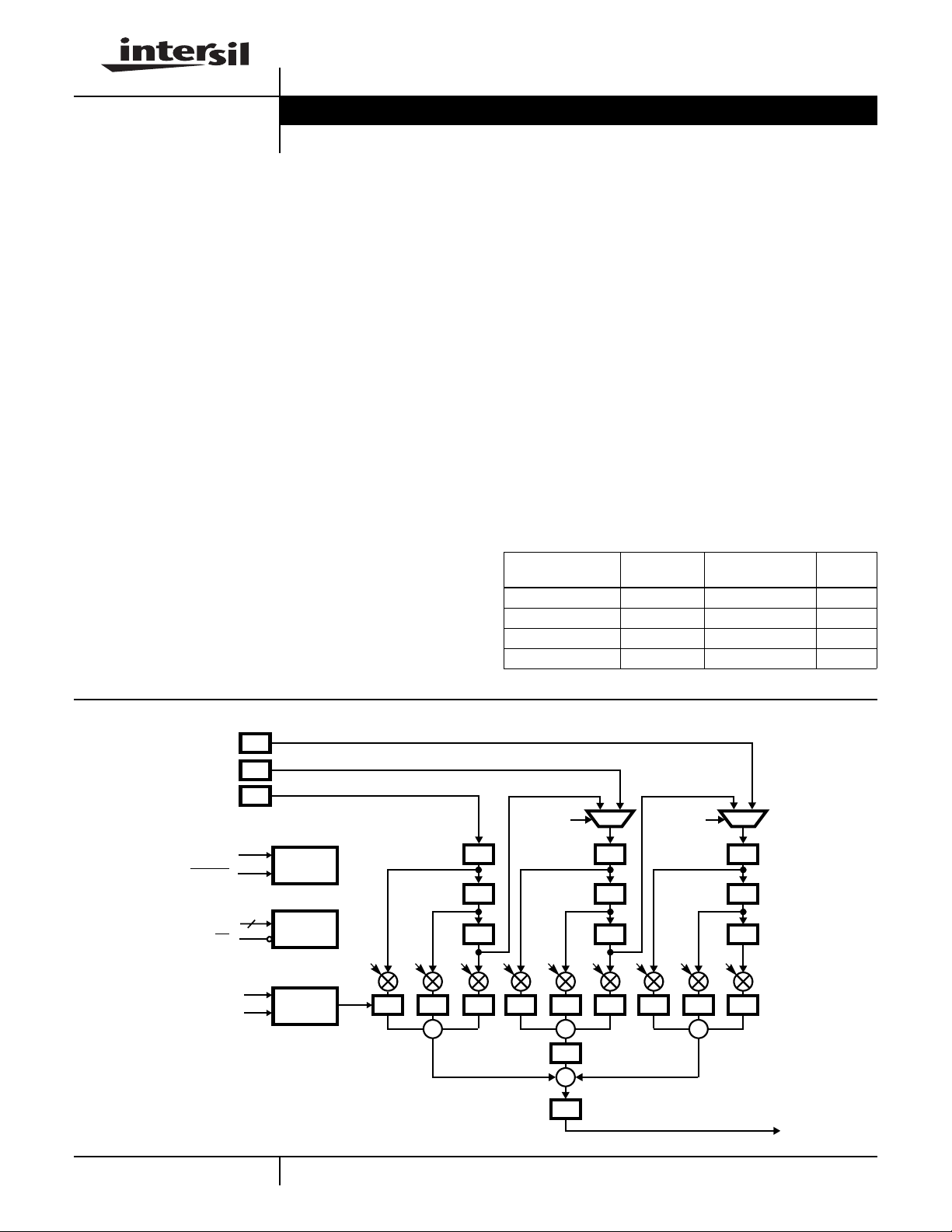
Block Diagram
DIN3 (0-7)
DIN2 (0-7)
DIN1 (0-7)
FRAME
CIN0-7
A0-2
LD
CLK
HOLD
-1
Z
-1
Z
-1
Z
3
CONTROL
LOGIC
ADDRESS
DECODER
INTERNAL
CLOCK
CLOCK
GEN
MODE MODE
-1
Z
-1
Z
-1
Z
-1
-1
-1
Z
Z
Z
+ + +
-1
Z
2:1
-1
Z
-1
Z
-1
Z
-1
-1
-1
Z
-1
Z
+
-1
Z
Z
Z
2:1
-1
Z
-1
Z
-1
Z
ABCDEFGHI
-1
-1
Z
Z
DOUT 0-19
1
CAUTION: These devices are sensitive to electrostatic discharge; follow proper IC Handling Procedures.
http://www.intersil.com or 407-727-9207 | Copyright © Intersil Corporation 1999
Page 2
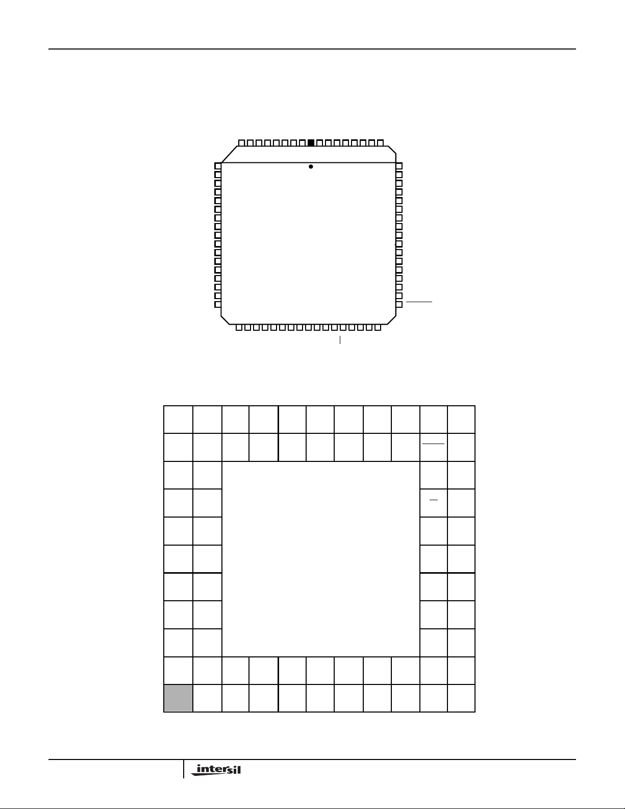
Pinouts
HSP48901
68 LEAD PLCC
TOP VIEW
DOUT3
A2A1A0
HOLD
DOUT4
DOUT5
4327 28 29 30 31 32 33 34 35 36 37 38 39 40 41 42
CC
V
DOUT6
60
DOUT7
59
DOUT8
58
DOUT9
57
GND
56
DOUT10
55
DOUT11
54
DOUT12
53
DOUT13
52
DOUT14
51
DOUT15
50
DOUT16
49
DOUT17
48
DOUT18
47
DOUT19
46
V
45
CC
FRAMES
44
DIN2 (7)
DIN2 (6)
DIN2 (5)
DIN2 (4)
DIN2 (3)
DIN2 (2)
DIN2 (1)
DIN2 (0)
GND
DIN3 (7)
DIN3 (6)
DIN3 (5)
DIN3 (4)
DIN3 (3)
DIN3 2)
DIN3 (1)
DIN3 (0)
VCCDIN1 (0)
DIN1 (1)
DIN1 (2)
DIN1 (3)
DIN1 (4)
DIN1 (5)
DIN1 (6)
DIN1 (7)
GND
DOUT0
DOUT1
DOUT2
9 8 7 6 5 4 3 2 1 6867666564636261
10
11
12
13
14
15
16
17
18
19
20
21
22
23
24
25
26
CC
V
CLK
GND
CIN7
CIN6
CIN5
CIN4
CIN3
CIN2
CIN1
CIN0
GND
LD
68 PIN GRID ARRAY (PGA)
TOP VIEW
11
DOUT6
DOUT7
DOUT9
DOUT10
DOUT12
DOUT14
DOUT16
DOUT18
V
CC
10
DOUT5
9
DOUT3
8
DOUT1
7
GND
DIN1 (6)
6
5
DIN1 (4)
4
DIN1 (2)
3
DIN1 (0)
2
V
CC
1
V
CC
DOUT4
DOUT2
DOUT0
DIN1 (7)
DIN1 (5)
DIN1 (3)
DIN1 (1)
DIN2 (7)
DIN2 (6)
BCDEFGHJKLA
DOUT6
DIN2 (5)
DIN2 (4)
GND
DIN2 (3)
DIN2 (2)
DOUT11
DIN2 (1)
DIN2 (0)
DOUT13
GND
DIN2 (7)
DOUT15
DIN3 (6)
DIN3 (5)
DOUT17
DIN3 (4)
DIN3 (3)
DOUT19
DIN3 (2)
DIN3 (1)
FRAME
A2
LD
CIN0
CIN2
CIN4
CIN6
GND
V
CC
DIN3 (0)
A0
A1
HOLD
GND
CIN1
CIN3
CIN5
CIN7
CLK
2
Page 3
HSP48901
Pin Descriptions
NAME PLCC PIN TYPE DESCRIPTION
V
CC
GND 18, 29, 38, 56 The device ground.
CLK 28 I Input and System clock. Operations are synchronous with therising edgeof this clock signal.
DIN1(7-0) 1-8 I Pixel Data Input Bus #1. These inputs are used to provide 8-bit pixel data to the HSP48901.
DIN2(7-0) 10-17 I Pixel Data Input Bus #2. Same as above. These inputs should be grounded when operating
DIN3(7-0) 19-26 I Pixel Data Input Bus #3. Same as above. These inputs should be grounded when operating
CIN7-0 30-37 I Coefficient Data Input Bus. This input bus is used to load the Coefficient Mask Register(s)
DOUT19-0 46-55, 57-60,
FRAME 44 I FRAME is an asynchronous new frame or vertical sync input. A low on this input resets all
HOLD 40 I The Hold Input is used to gate the clock from all of the internal circuitry of the HSP48901.
A2-0 41-43 I Control RegisterAddress. These linesare decodedto determine whichregister in thecontrol
LD 39 I Load Strobe. LD is usedfor loading the Internal Registers of theHSP48901. The rising edge
9, 27, 45, 61 The +5V power supply pins. 0.1µF capacitors between the VCC and GND pins are
recommended.
The data must be provided in a synchronous fashion, andis latched on the rising edge of the
CLK signal. The DIN1(0-7) inputs are also used to input data when operating in the 9-Tap
FIR mode.
in the 1D mode.
in the 1D mode.
and the Initialization Register. The register to be loaded is defined by the register address
bits A0-2. The CIN0-7 data is loaded to the addressed register through the use of the LD
input.
O Output Data Bus. This 20-Bit output port is used to provide the convolution result. The result
62-67
is the sum of products of the input data samples and their corresponding coefficients.
internalcircuitry except for the Coefficientand INT Registers. Thus, aftera FRAME resethas
occurred, a new frame of pixels may be convolved without reloading these registers.
This signal is synchronous, is sampled on the rising edge of CLK and takes effect on the
following cycle. While this signal is active (high), the clock will have no effect on the
HSP48901 and internal data will remain undisturbed.
logic is the destination for the data on the CIN0-7 inputs. Register loading is controlled by
the A0-2 and LD inputs.
of LD will latch the CIN0-7 data into the register specified by A0-2. The Address on A0-2
must be setup with respect to the falling edge of LD and must be held with respect to the
rising edge of LD.
3
Page 4

HSP48901
Functional Description
The HSP48901 can perform convolution of a 3 x 3 filter kernel
with 8-bit image data. It accepts the image data in a raster
scan, non-interlaced format, convolves it with the filter k ernel
and outputs the filtered image. The input and filter kernel data
are both 8-bits, while the output data is 20 bits to prevent
overflowduring the convolution operation. Image data is input
via the DIN1, DIN2, and DIN3 busses. This data would
normally be provided by programmable data buffer such as
the HSP9501 as illustrated in the Operations Section of this
specification. The data is then convolved with the 3 x 3 arr ay
of filter coefficients. The resultant output data is then stored in
the Output Register. The HSP48901 ma y also be used in a
one-dimensional mode. In this configuration, it functions as a
1-D 9-tap FIR filter. Data would be input via the DIN1(0-7) bus
for operation in this mode.
Initialization of the convolveris done using the CIN0-7 bus to
load configuration data and the filter kernel(s). The address
lines A0-2 are used to address the Internal Registers for
initialization. The configuration data is loaded using the
A0-2, CIN0-7 and
enable, respectively. This interface is compatible with
standard microprocessors without the use of any additional
glue logic.
Filtered image data is output from the convolver over the
DOUT0-19 bus. This output bus is 20 bits wide to provide
room for growth during the convolution operation.
LD controls as address, data and write
8-Bit Multiplier Array
The multiplier array consists of nine 8 x 8 multipliers. Each
multiplier forms the product of a filter coefficient with a
corresponding pixel in the input image. Input and coefficient
data may be in either two's complement or unsigned integer
format. The nine coefficients form a 3 x 3 filter kernel which
is multiplied by the input pixel data and summed to form a
sum of products for implementation of the convolution
operation as shown below:
FILTER KERNEL INPUT DATA
A B C P1P2P3
D E F P4P5P6
G H I P7P8P9
OUTPUT = (A x P1) + (B x P2) + (C x P3)
+ (D x P4) + (E x P5) + (F x P6)
+ (G x P7) + (H x P8) + (I x P9)
Control Logic
The control logic (Figure 1) contains the Initialization
Register and the Coefficient Registers. The control logic is
updated by placing data on the CIN0-7 bus and using the
A0-2 and
(see Address Decoder). All of the Control Logic Registers
are unaffected by
LD control lines to write to the addressed register
FRAME.
A0 - 2
LD
CIN0 - 7
CR1
ENCR1
ENCR0
3
SQ
C Q
ENCRO
ADDRESS
CODE
INITIALIZATION REGISTER
CAS
(INT)
I0
E H0 E G0 EF0EE0E
IHGFEDCBA
I1 E H1 E G1 EF1EE1E
FIGURE 1. CONTROL LOGIC BLOCK DIAGRAM
ENCR1
CAS
CR1
CRO
INITIALIZATION
DAT A
COEFFICIENT
REGISTER 0
COEFFICIENT
REGISTER 1
D1
D0
C0
E
E
EB0E A0 ECR0
C1
EB1E A1 E
4
Page 5

HSP48901
Initialization Register
The Initialization Register is used to appropriately configure
the convolverfor a particularapplication. It is loaded through
the use of the CIN0-7 bus along with the
defines the input data and coefficients format (unsigned or
two's complement); Bit-1 defines the mode of operation (1-D
or 2-D); and Bit-2 and Bit-3 determine the type of rounding to
occur on the DOUT0-19 bus; The complete definition of the
Initialization Register bits is given in Table 1.
TABLE 1. INITIALIZATION REGISTER
INITIALIZATION REGISTER
FUNCTION = INPUT AND COEFFICIENT
BIT 0
0 Unsigned Integer Format
1 Two’s Complement Format
BIT 1 FUNCTION = OPERATING MODE
0 1-D 9-Tap Filter
1 2-D 3 x 3 Filter
3 BIT 2 FUNCTION = OUTPUT ROUNDING
0 0 No Rounding
0 1 Round to 16 Bits (i.e., DOUT19-4)
1 0 Round to 8 Bits (i.e., DOUT19-12)
1 1 Not Valid
DATA FORMAT
Coefficient Registers (CREG0, CREG1)
The control logic contains two coefficient register banks,
CREG0 and CREG1. Each of these register banks is
capable of storing nine 8-bit filter coefficient values (3 x 3
Kernel). The output of the registers are connected to the
coefficient input of the corresponding multiplier in the 3 x 3
multiplier array (designated A through I). The register bank
to be used for the convolution is selectable by writing to the
appropriate address (see address decoder). All registers in a
given bank are enabled simultaneously, and one of the
banks is always active.
For most applications, only one of the register banks is
necessary.The user can simply load CREG0 after power up,
and use it forthe entire convolution operation. (CREG0 is the
Default Register). The alternate register bank allows the
user to maintain two sets of filter coefficients and switch
between them in real time. The coefficient masks are loaded
via the CIN0-7 bus by using A0-2 and
the particular register bank to be used in processing is also
done by writing to the appropriate address (See address
decoder). For example, if CREG0 is being used to provide
coefficients to the multipliers, CREG1 can be updated at a
low rate by an external processor; then, at the proper time,
CREG1 can be selected, so that the new coefficient mask is
used to process the data. Thus, no clock cycles have been
lost when changing between alternate 3 x 3 filter kernels.
LD input. Bit-0
LD. The selection of
The nine coefficients must be loaded sequentially over the
CIN0-7 bus from A to I. The address of CREG0 or CREG1 is
placed on A0-2, and then the coefficients are written to the
corresponding Coefficient Register one at a time by using
the
LD input.
Address Decoder
The address decoder (see Figure 1) is used for writing to the
control logic of the HSP48901. Loading an Internal Register
is done by selecting the Destination Register with the A0-2
address lines, placing the data on CIN0-7, and asserting
control line. When
LD goes high, the data on ClN0-7 is
latched into the addressed register. The address map for the
A0-2 bus is shown in Table 2.
While loading of the control logic registers is asynchronous
to CLK, the target register in the control logic is being read
synchronous to the internal clock. Therefore, care must be
taken when modifying the convolver setup parameters
during processing to avoid changing the contents of the
registers near a rising edge of CLK. The required setup time
relative to CLK is given by the specification TLCS. For
example, in order to change the active coefficient register
from CREG0 to CREG1 during an active convolution
operation, a write will be performed to the address for
selecting CREG1 for internal processing (A0-2 = 110). In
order to provide proper uninterrupted operation,
LD should
be deasserted at least TLCS prior to the next rising edge of
CLK. Failure to meet this setup time may result in
unpredictable results on the output of the convolver. Keep in
mind that this requirement applies only to the case where
changes are being made in the control logic duringan active
convolution operation. In a typical convolver configuration
routine, where the configuration data is loaded prior to the
actual convolution operation, this specification would not
apply.
TABLE 2. ADDRESS MAPS
CONTROL LOGIC ADDRESS MAP
A2-0 FUNCTION
0 0 0 Reserved for Future Use.
0 0 1 Reserved for Future Use.
0 1 0 Load Coefficient Register 0 (CREG0).
0 1 1 Load Coefficient Register 1 (CREG1).
1 0 0 Load Initialization Register (INT).
1 0 1 Select CREG0 for Internal Processing.
1 1 0 Select CREG1 for Internal Processing.
1 1 1 No Operation.
LD
5
Page 6

HSP48901
Control Signals
HOLD
The HOLD control input provides the ability to disable
internal clock and stop all operations temporarily. HOLD is
sampled on the rising edge of CLK and takes effect during
the following clock cycle (refer to Figure 2). This signal can
be used to momentarily ignore data at the input of the
convolver while maintaining its current output data and
operational state.
CLK
HOLD
INTERNAL
CLOCK
FIGURE 2. HOLD OPERATION
FRAME
The FRAME input initializes all internal flip flops and
registers except for the coefficient and Initialization
Registers. It is used as a reset between video frames and
eliminates the need to reinitialize the entire HSP48901 or
reload the coefficients. The registers and flip flops will
remain in a reset state as long as
is an asynchronous input and may occur at any time.
However, it must be deasserted at least t
rising clock edge that is to begin operation for the next frame
in order to ensure the new pixel data is properly loaded.
Operation
A single HSP48901 can be used to perform 3 x 3 convolution
on 8-bit image data. A Block Diagram of this configuration is
shown in Figure 3. The inputs of an external data buffer (such
as the HSP9501) are connected to the input data in parallel
with the DlN1(0-7) lines; the outputs of the data buffer are
connected tothe DIN2(0-7) bus. Asecond external data buffer
is connected between the outputs of the first buffer and the
DIN3(0-7) inputs. To perform the convolution operation, a
group of nine image pixels is multiplied by the 3 x 3 arr ay of
filter coefficients and their products are summed and sent to
the output. For the example in Figure 3, the pixel value in the
output image at location m, n is given by:
DOUT(m,n) = A x Pm-1, n-1 + B x Pm-1,n +C x Pm-1, n+1
+ D x Pm, n-1 + E x Pm, n + F x Pm, n+1
+ G x Pm+1,n-1 + H x Pm+1,n +I xPm+1, n+1
This process is continually repeated until the last pixel of the
last row of the image has been input. It can then start again
with the first row of the next frame. The
clear the Internal Multiplier Registers and DOUT0-19
Registers between frames. The row length of the image to be
convolved is limited only by the maximum length of the
external data buffers.
The setup is straightforward. The user must first setup the
HSP48901 by loading a new value into the Initialization
FRAME is active. FRAME
ns prior to the
FS
FRAME pin is used to
Register. The coefficients can now be loaded one at a time
from A to I via the CIN0-7 coefficient bus, and the A0-2 and
LD control lines.
DAT A
BUFFER
DAT A
BUFFER
A
B
D
E
F
H
8
DAT A
C
F
I
DIN 1 (0 -7)
DOUT 0 -19
DIN 2 (0 -7)
HSP48901
DIN 3 (0 -7)
P
M -1, N -1PM -1, NPM -1, N +1
P
M, N -1
P
M+1, N -1PM+1, NPM+1, N +1
P
20
M, N
FILTERED
IMAGE
DAT A
P
M, N +1
IMAGE
DAT A
INITIALIZATION
FILTER KERNEL IMAGE DATA
FIGURE 3. 3 x 3 KERNEL ON AN 8-BIT IMAGE
Multiple filter kernels can also be used on the same image
data using the dual Coefficient Registers CREG0 and
CREG1. This type of filtering is used when the characteristics
of the input pixel data change over the image in such a w ay
that no one filter produces satisfactory results for the entire
image. In order to filter such an image, the characteristics of
the filter itself must change while the image is being
processed. The HSP48901 can perform this function with the
use of an external processor. The processor is used to
calculate the required new filter coefficients, loads them into
the Coefficient Register not in use, and selects the newly
loaded Coefficient Register at the proper time. The first
Coefficient Register can then be loaded with new coefficients
in preparation for the next change . This can be carried out
with no interruption in processing, provided that the new
register is selected synchronous to the convolver CLK signal.
The HSP48901 can also operate as a one dimensional 9-tap
FIR filter by programming the Initialization Register to 1-D
mode (i.e., INT bit-1 = 0). This configuration will provide for
nine sequential input values to be multiplied by the coefficient
values in the selected Coefficient Register and provide the
proper filtered output. The input bus to be used when
operating in this mode is the DIN1(0-7) inputs.
The equation for the output in the 1-D 9-tap FIR case
becomes:
D0UTn = A x Dn-8 + B x Dn-7 + C x Dn-6 + D x Dn-5
+ E x Dn-4 + F x Dn-3 + G x Dn-2 + H x Dn-1
+ l x Dn
Frame Rate
The total time to process an image is given by the formula:
T = R x C/F, where:
T = Time to process a frame
R = Number of rows in the image
C = Number of pixels in a row
F = Clock rate of the HSP48901
6
Page 7

HSP48901
Absolute Maximum Ratings Thermal Information
Supply Voltage. . . . . . . . . . . . . . . . . . . . . . . . . . . . . . . . . . . . . +8.0V
Input, Output or I/O Voltage Applied . . . . .GND -0.5V to VCC +0.5V
ESD Classification . . . . . . . . . . . . . . . . . . . . . . . . . . . . . . . . .Class 1
Operating Conditions
Voltage Range. . . . . . . . . . . . . . . . . . . . . . . . . . . . . .4.75V to 5.25V
Temperature Range . . . . . . . . . . . . . . . . . . . . . . . . . . . .0oC to 70oC
CAUTION: Stresses above those listed in “Absolute Maximum Ratings” may cause permanent damage to the device. This is a stress only rating and operationofthe
device at these or any other conditions above those indicated in the operational sections of this specification is not implied.
NOTE:
1. θJA is measured with the component mounted on an evaluation PC board in free air.
Thermal Resistance (Typical, Note 1) θJA (oC/W) θJC (oC/W)
PLCC Package. . . . . . . . . . . . . . . . . . . 43 N/A
PGA Package. . . . . . . . . . . . . . . . . . . . 38 8
Maximum Junction Temperature
PLCC Package. . . . . . . . . . . . . . . . . . . . . . . . . . . . . . . . . . .150oC
PGA Package. . . . . . . . . . . . . . . . . . . . . . . . . . . . . . . . . . . .175oC
Maximum Storage Temperature Range. . . . . . . . . . -65oC to 150oC
Maximum Lead Temperature (Soldering 10s) . . . . . . . . . . . . .300oC
(PLCC - Lead Tips Only)
Die Characteristics
Number of Transistors or Gates. . . . . . . . . . . . . . . . . . 13,594 Gates
DC Electrical Specifications V
= 5.0V ±5%, TA = 0oC to 70oC
CC
PARAMETER SYMBOL TEST CONDITIONS MIN MAX UNITS
Logical One Input Voltage V
Logical Zero Input Voltage V
High Level Clock Input V
Low Level Clock Input V
Output HIGH Voltage V
Output LOW Voltage V
Input Leakage Current I
Standby Power Supply Current I
CCSB
IHC
VCC = 5.25V 2.0 - V
IH
VCC = 4.75V - 0.8 V
IL
VCC = 5.25V 3.0 - V
VCC = 4.75V - 0.8 V
ILC
IOH = 400µA, VCC = 4.75V 2.6 - V
OH
IOL = +2.0mA, VCC = 4.75V - 0.4 V
OL
VIN = VCC or GND, VCC = 5.25V -10 10 µA
I
VIN = VCC or GND, VCC = 5.25V,
Outputs Open
Operating Power Supply Current I
CCOP
f = 20MHz, VIN=VCCor GND, VCC= 5.25V
(Note 2)
Input Capacitance C
f = 1MHz, VCC = Open, All Measurements
IN
are referenced to device GND (Note 3).
Output Capacitance C
O
NOTES:
2. Power supply current is proportional to operating frequency. Typical rating for I
CCOP
3. Not tested, but characterized at initial design and at major process/design changes.
- 500 µA
- 120 mA
-10pF
-15pF
is 6mA/MHz.
AC Electrical Specifications V
PARAMETER SYMBOL NOTES
Clock Period t
Clock Pulse Width High t
Clock Pulse Width Low t
Data Input Setup Time t
Data Input Hold Time t
Clock to Data Out t
Address Setup Time t
CYCLE
PWH
PWL
DS
DH
OUT
7
= 5.0V ±5%, TA = 0oC to 70oC
CC
CONDITIONS
AS
TEST
-30 -40
UNITSMIN MAX MIN MAX
33-50-ns
13-20-ns
13-20-ns
14-16-ns
0-0-ns
- 21 - 30 ns
5-5-ns
Page 8

HSP48901
AC Electrical Specifications V
PARAMETER SYMBOL NOTES
Address Hold Time t
Configuration Data Setup Time t
Configuration Data Hold Time t
LD Pulse Width t
LD Setup Time t
HOLD Setup Time t
HOLD Hold Time t
FRAME Pulse Width t
FRAME Setup Time t
Output Rise t
Output Fall Time t
= 5.0V ±5%, TA = 0oC to 70oC
CC
AH
CS
CH
LPH
LCS
HS
HH
FPW
FS
R
F
Note 4 31 t
Note 5 28 - 40 - ns
From 0.8V to 2.0V - 8 - 8 ns
From 2.0V to 0.8V - 8 - 8 ns
TEST
CONDITIONS
-30 -40
UNITSMIN MAX MIN MAX
2-2-ns
10-12-ns
0-0-ns
13-20-ns
+2 40 t
CYCLE
CYCLE
+2 ns
10-12-ns
0-0-ns
t
CYCLE
-t
CYCLE
-ns
NOTES:
4. This specification applies only to the case where a change in the active Coefficient Register is being selected duringa convolutionoperation. It must
be met in order to achieve predictable results at the next rising clock edge. In most applications, this selection will be made asynchronously, and the
t
Specification may be disregarded.
LCS
5. While FRAME isasynchronous with respect to CLK, it must be deasserteda minimum of tFSns prior to the rising clock edge which isto begin loading
new pixel data for the next frame.
6. AC Testingis performed as follows: Input levels(CLK Input) = 4.0V and 0V; input levels (all other inputs) = 0V to 3.0V; input timing reference levels:
(CLK) = 2.0V, (others) = 1.5V; other timing references: VOH≥ 1.5V, VOL≤ 1.5V; output load test load circuit with CL = 40pF.
Test Load Circuit
(NOTE 7) C
NOTES:
7. Includes stray and jig capacitance.
8. Switch S1 Open for I
CCSB
and I
DUT
CCOP
L
Tests.
S
1
I
OH
EQUIVALENT CIRCUIT
1.5V I
±
OL
8
Page 9

Timing Waveforms
t
CLK
DIN 0-7
PWL
HSP48901
t
CYCLE
t
PWH
t
DS
t
DH
LD
A0-2
t
AS
t
LPW
t
AH
t
OUT
DOUT 0-19
CIN0-7
FIGURE 4. FUNCTIONAL TIMING FIGURE 5. CONFIGURATION TIMING
CLK
t
CLK
LD
t
LCS
HOLD
INTERNAL
CLOCK
HS
FIGURE 6. SYNCHRONOUS LOAD TIMING FIGURE 7. HOLD TIMING
t
FRAME
FPW
t
CS
t
HH
t
HS
t
CH
t
FS
CLK
FIGURE 8. FRAME TIMING
All Intersil semiconductor products are manufactured, assembled and tested under ISO9000 quality systems certification.
Intersil semiconductor products are sold by description only.Intersil Corporation reserves the right to make changes in circuit design and/or specifications at any time without notice. Accordingly ,the reader is cautioned to verify that data sheets are current before placing orders. Information furnished by Intersil is believed to be accurate and
reliable. However, no responsibility is assumed by Intersil or its subsidiaries for its use; nor for any infringements of patents or other rights of third parties which may result
from its use. No license is granted by implication or otherwise under any patent or patent rights of Intersil or its subsidiaries.
For information regarding Intersil Corporation and its products, see web site http://www.intersil.com
9
 Loading...