

Page 1
HSP45240
September 1997
Features
• Block Oriented 24-Bit Sequencer
• Configurable as Two Independent 12-Bit Sequencers
• 24 x 24 Crosspoint Switch
• Programmable Delay on 12 Outputs
• Multi-Chip Synchronization Signals
• Standard µP Interface
• 100pF Drive on Outputs
• DC to 50MHz Clock Rate
Applications
• 1-D, 2-D Filtering
• Pan/Zoom Addressing
• FFT Processing
• Matrix Math Operations
Ordering Information
TEMP.
PART NUMBER
HSP45240JC-33 0 to 70 68 Ld PLCC N68.95
HSP45240JC-40 0 to 70 68 Ld PLCC N68.95
HSP45240JC-50 0 to 70 68 Ld PLCC N68.95
HSP45240GC-33 0 to 70 68 Ld PGA G68.A
HSP45240GC-40 0 to 70 68 Ld PGA G68.A
HSP45240GC-50 0 to 70 68 Ld PGA G68.A
RANGE (oC) PACKAGE
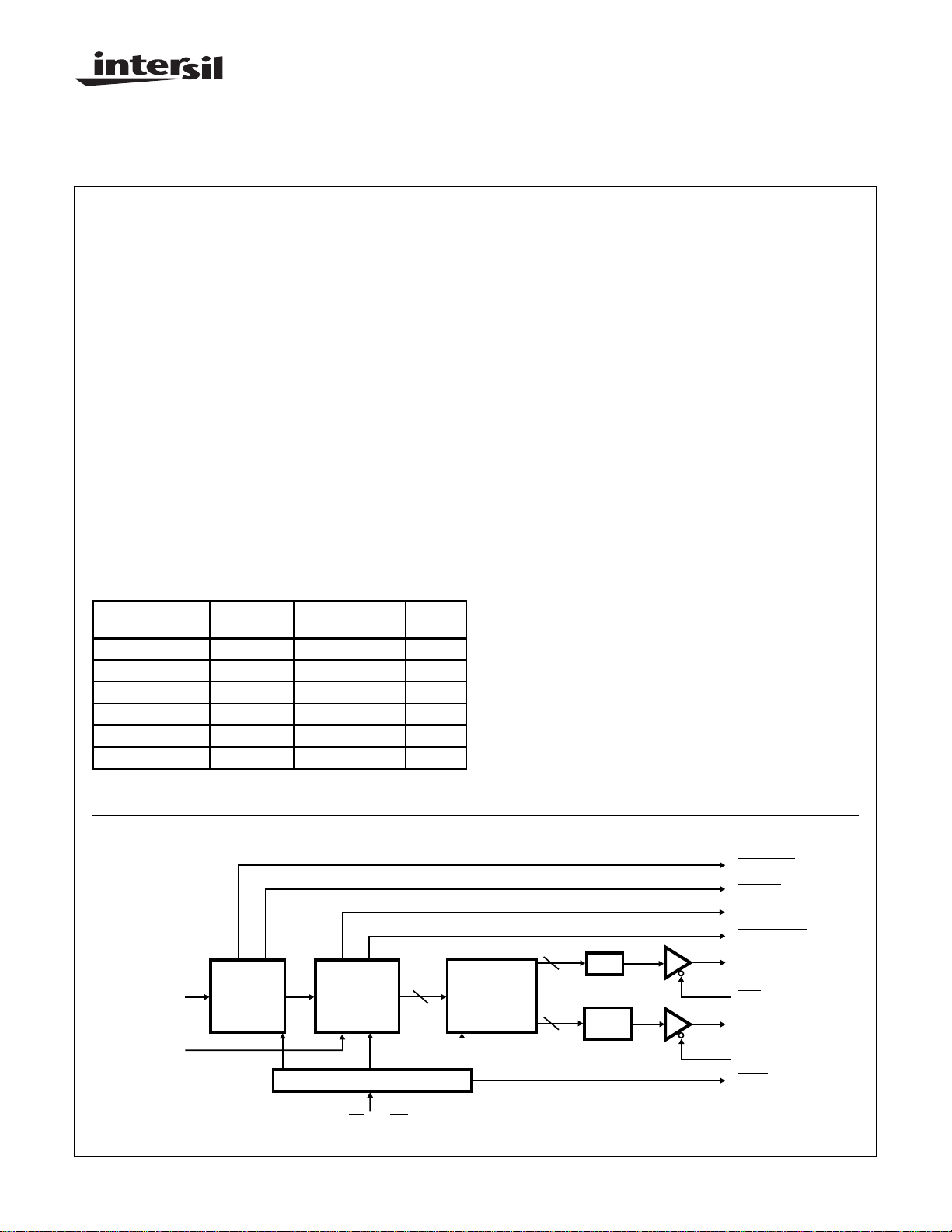
Address Sequencer
Description
The Intersil HSP45240 is a high speed Address Sequencer
which provides specialized addressing for functions like
FFTs, 1-D and 2-D filtering, matrix operations, and image
manipulation. The sequencer supports block oriented
addressing of large data sets up to 24-bits at clock speeds
up to 50MHz.
Specialized addressing requirements are met by using the
onboard 24 x 24 crosspoint switch. This feature allows the mapping of the 24 address bits at the output of the address generator to the 24 address outputs of the chip. As a result, bit rev erse
addressing, such as that used in FFTs, is made possible.
A single chip solution to read/write addressing is also made
possible by configuring the HSP45240 as two 12-bit
sequencers. To compensate for system pipeline delay, a programmable delay is provided on 12 of the address outputs.
The HSP45240 is manufactured using an advanced CMOS
process, and is a low power fully static design. The configuration of the device is controlled through a standard microprocessor interface and all inputs/outputs, with the e xception
of clock, are TTL compatible.9-
PKG.
NO.
Block Diagram
12
STARTIN
DLYBLK
CAUTION: These devices are sensitive to electrostatic discharge; follow proper IC Handling Procedures.
http://www.intersil.com or 407-727-9207
START
CIRCUITRY
SEQUENCE
GENERATOR
PROCESSOR INTERFACE
CS, A0, WR
D0-6,
| Copyright © Intersil Corporation 1999
24
CROSSPOINT
SWITCH
9-1
12
REG
DELAY
1-8
STARTOUT
ADDVAL
DONE
BLOCKDONE
OUT12-23
OEH
OUT0-11
OEL
BUSY
File Number 2489.3
Page 2
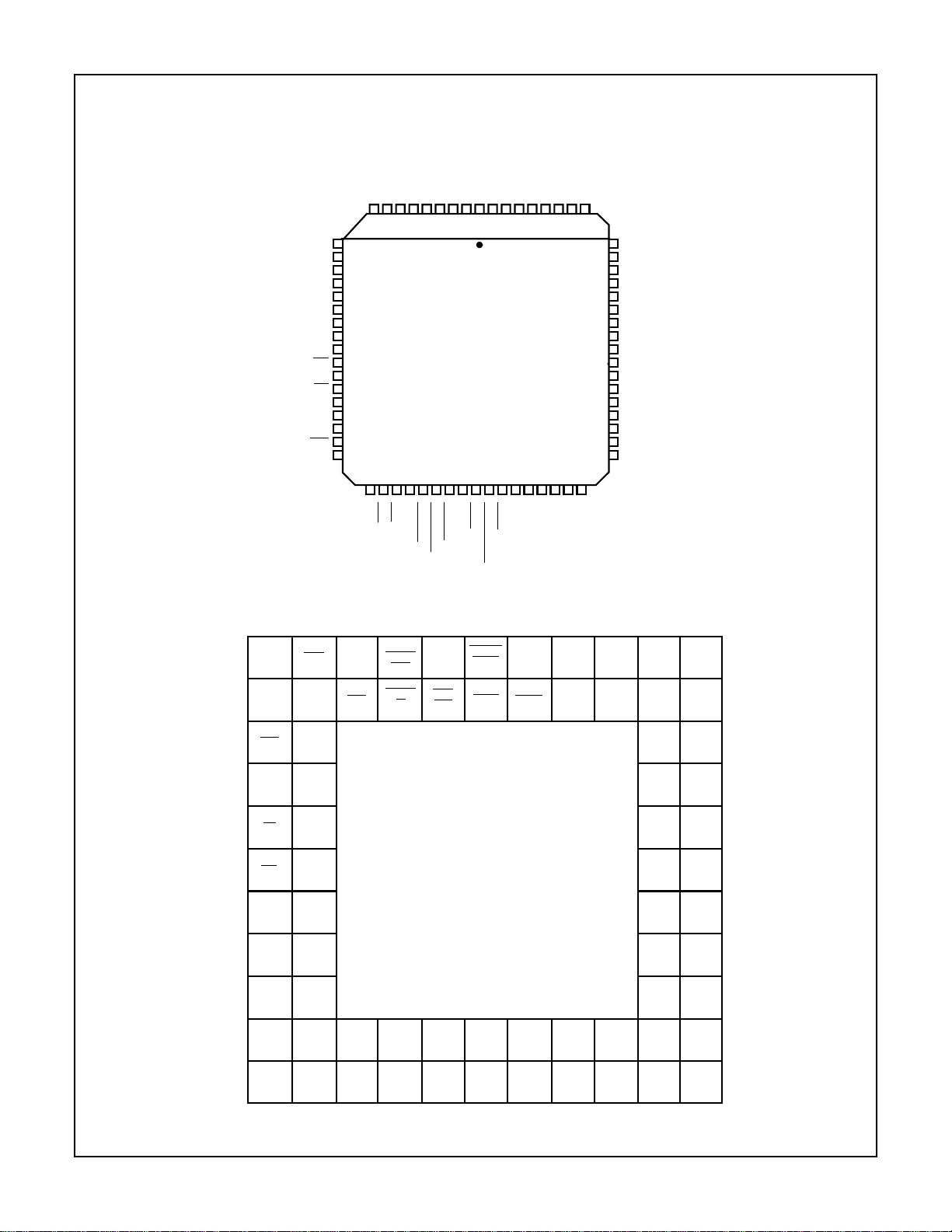
Pinouts
HSP45240
ADDRESS SEQUENCER HSP45240
68 PIN PLASTIC LEADED CHIP CARRIER (PLCC)
GND
OUT23
OUT22
VCCOUT21
OUT20
GND
OUT19
OUT18
VCCOUT17
OUT16
GND
OUT15
9876543216867666564636261
NC
10
D0
11
D1
12
D2
13
D3
14
15
D4
16
D5
17
D6
18
GND
19
WR
20
A0
21
CS
22
GND
23
CLK
24
V
CC
25
RST
26
NC
OUT14
OUT13
4327 2829 30 31 32 33 34 35 36 37 38 39 40 41 42
NC
NC
60
OUT12
59
GND
58
OUT11
57
OUT10
56
V
55
CC
OUT9
54
OUT8
53
GND
52
OUT7
51
OUT6
50
V
49
CC
OUT5
48
OUT4
47
GND
46
OUT3
45
NC
44
NC
OEH
OEL
DLYBLK
STARTIN
STARTOUT
ADDVAL
CC
V
BUSY
GND
OUT0
DONE
BLOCKDONE
OUT1
CC
NC
V
OUT2
68 PIN GRID ARRAY (PGA)
BOTTOM VIEW
V
CC
ADD
VAL
BLOCK
DONE
BUSY
GND
DONE
OUT1
OUTO
OUT2
V
CC
NC
NC
GND
OUT5
OUT6
GND
OUT9
OUT10
OUT3
OUT4
V
CC
OUT7
OUT8
V
CC
OUT11
OEL
START
OUT
START
IN
L
K
J
H
G
F
E
D
NC
RST
CLK
CS
WR
D6
D4
OEH
NC
V
CC
GND
A0
GND
D5
D3
DLYBLK
OUT12
D2
C
B
A
D1
D0
NC
GND
2345678910111
OUT22
OUT23
OUT21
GND
OUT18
OUT17
OUT20
V
CC
OUT19
GND
OUT14
V
OUT16
CC
OUT15
GND
NC
OUT13
NC
9-2
Page 3
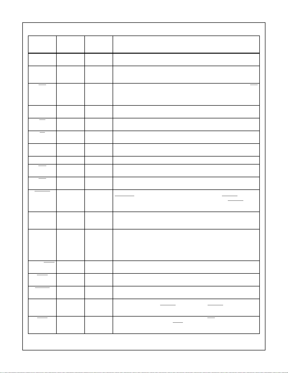
Pin Descriptions
NAME TYPE
HSP45240
PLCC
PIN
NUMBER DESCRIPTION
V
CC
GND I 3, 9, 18, 22,
RST I 25 RESET: This active low input causes a chip reset which lasts for 26 clocks after RST
CLK I 23 CLOCK: The “CLK” signal is a CMOS input which provides the basic timing for address
WR I 19 WRITE: The rising edge of this input latches the data/address on D0-6 to be latched
CS I 21 CHIP SELECT: This active “low” input enables the configuration data/address on
A0 I 20 ADDRESS 0: This input defines D0-6 as a configuration register address if “high”, and
D0-6 I 11-17 DATA BUS: Data bus for Processor Interface.
OEH I 28 OUTPUT ENABLE HIGH: This asynchronous input is used to enable the output buffers
OEL I 29 OUTPUT ENABLE LOW: This asynchronous input is used to enable the output buffers
STARTIN I 31 START-IN: This active low input initiates an addressing sequence. May be tied to
DLYBLK I 30 DELA Y BLOCK: This activ e “high” input ma y be used to halt address gener ation on ad-
OUT0-23 O 39, 40, 42, 45,
BLOCK DONE O 36 BLOCK DONE: This active low output signals when the last address in an address block
DONE O 37 DONE: This active low output signals when the last address of an address sequence is
ADDVAL O 33 ADDRESS VALID: This active low output signals when the first address of an address
START-OUT O 32 ST ART-OUT: This active lo w output is generated when an address sequence is initiated
BUSY O 35 BUSY: This active low output is asserted one CLK after RST is deasserted and will re-
NOTE: #Denotes active low.
I 6, 24, 34, 41
49, 55, 68
38, 46, 52,
58, 65
47, 48, 50, 51,
53, 54, 56, 57,
59, 62-64, 66,
67, 1, 2, 4, 5,
7, 8
+5V power supply pin.
GROUND.
has been deasserted. The reset initializes the Crosspoint Switch and some of the configuration registers as described in the Processor Interface Section. The chip must be
clocked for reset to complete.
generation.
into the Processor Interface.
D0-6 to be latched into the Processor Interface.
configuration data if “low”, (see Processor Interface text).
for OUT 12-23.
for OUT0-11.
STARTOUT of another H5P45240 for multichip synchronization. STARTIN should only
be asserted for one CLK because address sequencing begins after STARTIN is deasserted.
dress block boundaries (see Sequence Generator text). The required timing relationship of this signal to the end of an address block is shown in Application Note 9205.
OUTPUT BUS: TTL compatible 24-bit Address Sequencer output.
is on OUT0-23.
on OUT0-23.
sequence is on 0UT0-23.
by a mechanism other thanSTARTIN. Ma y be tied to theSTAR TIN of other H5P45240’ s
for multichip synchronization.
main asserted for 25 CLK’s. While BUSY is asserted, all writes to the Processor Interface are disabled.
9-3
Page 4
Functional Description
HSP45240
The Address Sequencer is a 24-bit programmable address
generator. As shown in the Block Diagram, the sequencer
consists of 4 functional blocks: the start circuitry, the
sequence generator, the crosspoint switch, and the processor interface. The addresses produced by the sequence
generator are input into the crosspoint switch. The crosspoint switch maps 24 bits of address input to a 24-bit output.
This allows for addressing schemes like “bit-reverse”
addressing for FFT’s. A programmable delay block is provided to allow the MSW of the output to be skewed from the
LSW . This feature may be used to compensate for processor
pipeline delay when the sequence generator is configured as
two independent 12-bit sequencers. Address Sequencer
operation is controlled by values loaded into configuration
registers associated with the sequence generator, crosspoint switch, and start circuitry. The configuration registers
are loaded through the processor interface.
Start Circuitry
The Start Circuitry generates the internal START signal
which causes the Sequence Generator to initiate an
addressing sequence. The START signal is produced by
writing the Processor Interface’s “Sequencer Start” address
(see Processor Interface text), by asserting the
input, or by the terminal address of a sequence generated
under “One-Shot Mode with Restart” (see Sequence Generator Section). Care should be taken to assert
only one clock cycle to ensure proper operation. A programmable delay from 1 to 31 clocks is provided to delay the initiation of an addressing sequence by delaying the internal
START signal (see Processor Interface text).
The Start Circuitry generates the output signal
which is asserted when the first valid output address is at the
pads. In addition, the Start Circuitry generates the
“
STARTOUT” signal for multichip synchronization. Note:
STARTOUT is only generated when an addressing
sequence is started by writing the “Sequencer Start”
address of the Processor Interface, or an internal START is
generated by reaching the end of an addressing sequence
produced by “One-Shot Mode with Restart”.
STARTlN
STARTlN for
ADDVAL
Sequence Generator
The Sequence Generator is a block oriented address generator. This means that the desired address sequence is subdivided into one or more address blocks, each containing a
user defined number of addresses. User supplied configuration data determines the number of address blocks and the
characteristics of the address sequence to be generated.
An address sequence is started when the control section of
the Sequence Generator receives the internal START signal
from the Start Circuitry. When the START signal is received,
the control section multiplexes the contents of the Start
Address Register and a “0” to the adder. The result of this
summation is the first address in the first block of the
address sequence. This value is stored in the Block Start
Address register by an enable generated from the control
section, and the multiplexers are switched to feed the output
of the Holding and Address Increment registers to the adder.
Address generation will continue with the Address Increment
added to the contents of the Holding Register until the first
address block has been completed.
An address block is completed when the number of
addresses generated since the beginning of the address
block equals the value stored in the Block Size register.
When the last address of the block is generated,
DONE is asserted to signal the end of the address block
(see Application Note 9205). On the following CLK, the multiplexers are configured to pass the contents of the Block
Start Address and Block Increment registers to the adder
which generates the first address of the next address block.
An enable from the control section allows this value to
update the Block Start Address register, and the multiplexers
are switched to feed the Holding and Address Increment registers to the adder for generation of the remaining addresses
in the block.
The address sequence is completed when the number of
address blocks generated equals the value loaded into the
Number of Blocks register. When the final address in the last
address block has been generated,
DONE are asserted to signal the completion of the address
sequence.
The parameters governing address generation are loaded
into five 24-bit configuration registers via the Processor
Interface. These parameters include the Start Address, the
beginning address of the sequence; the Block Size, the number of addresses in the address block; the Address Increment, the increment between addresses in a block; the
Number of Blocks, the number of address blocks in a
sequence (minimum 1); the Block Increment, the increment
between starting addresses of each block. The loading and
structure of these registers is detailed in the Processor Interface text.
DONE and BLOCK-
BLOCK-
As shown in Figure 1, the Sequence Generator is subdivided
into the address generation and control sections. The
address generation section performs an accumulation based
on the output of MUX1 and MUX2. The control section governs the operation of the multiplexers, enables loading of the
Block Start Address register, and signals completion of an
address sequence.
9-4
Page 5

CURRENT
BLOCK
START
ADDRESS
STEP SIZE
START
ADDRESS
BLOCK
STEP SIZE
HSP45240
R
E
G
R
E
G
R
E
G
R
E
G
“0”
“0”
M
U
X
1
M
U
X
2
A
D
D
E
R
12 MSB
12 LSB
12
M
U
X
HOLDING
REGISTER
12
R
E
G
24
TO
CROSSPOINT
SWITCH
ADDRESS
GENERATION
BLOCK
SIZE
NUMBER
OF
BLOCKS
MODE
R
E
G
R
E
G
R
E
G
TEST MODE
DAT A
FIGURE 1. SEQUENCE GENERATOR BLOCK
Three modes of operation may be selected by loading the 6-bit
Mode Control register (see Processor Interface). The three
modes of operation are:
1. One-Shot Mode without Restart Address generation halts
after completion of the user specified address sequence.
Address generation will not resume until the internal
ST AR T signal is generated by the Start Circuitry . When the
final address in the final block of the address sequence is
generated, both
DONE and BLOCKDONE are asserted
and the last address is held on OUT0-23 (See Application
Note 9205).
2. One-Shot Mode with Restart: This mode is identical to
One-Shot Mode without Restart with the exception that the
Start Circuitry automatically generates an inter nal START
at the end of the user specified sequence to restart address generation. The end of the address sequence is signaled by the assertion of
DONE, BLOCKDONE, and
STARTOUT as shown in Application Note 9205. In this
mode, the first address of the next sequence immediately
follows the last address of the current sequence if start delay is disabled.
3. Continuous Mode: Address generation never terminates.
Address generation proceeds based on the Start Address,
Address Increment, Block Size, and Block Increment Parameters. The Number of Blocks parameter is ignored, and
the
DONE signal is never asserted.
The Mode Control register is also used to configure the
Sequence Generator for operation as two independent 12-bit
address sequencers. In dual sequencer mode, the adder in
the sequence generator suppresses the carry from the 12
LSBs to the 12 MSBs. With the carry suppressed, two independent sequences may be produced. These 12-bit address
MUX CONTROLS/
REGISTER ENABLES
SEQUENCE
GENERATOR
CONTROL
“START”
CONTROL
DONE
BLOCKDONE
DLYBLK
sequences may be delay ed relativ e to each other b y prog ramming the Mode Control register for a delay up to 7 cloc ks . This
feature is useful to compensate for pipeline delay when using
dual sequencer mode to generate read/write addressing.
The DLYBLK input can be used to halt address generation at
the end of any address block within a sequence. In addition,
DLYBLK can be used to delay an address sequence from
restarting if asserted at the end of the final address bloc k generated under “One-Shot Mode with Restart”. See Application
Note 9205 for the timing relationship of DLYBLK to the end of
the address block required to halt address sequencing.
Crosspoint Switch
The crosspoint switch is responsible for reordering the
address bits output by the sequence generator. The switch
allows any of its 24 inputs to be independently connected to
any of its 24 outputs. The crosspoint switch outputs can be
driven by only one input, however, one input can drive any
number of switch outputs. If none of the inputs are mapped to
a particular output bit, that output will be “low”.
The input to output map is configured through the processor
interface. The I/O map is stored in a bank of 24 configuration
registers. Each register corresponds to one output bit. The
output bit is mapped to the input via a value, 0 to 23, stored in
the register. After power-up, the user has the option of configuring the switch in 1:1 mode by using the reset input, “
In 1:1 mode the crosspoint switch outputs are in the same
order as the input. More details on configuring the switch registers are contained in the Processor Interface text.
RST”.
9-5
Page 6

Processor Interface
HSP45240
The Processor Interface consists of a 10 pin microprocessor
interface and a register bank which holds configuration data.
The data is loaded into the register bank by first writing the
register address to the processor Interface and then writing
the data. An auto address increment mode is provided so that
a base address may be written followed by a number of data
writes.
The microprocessor interface consists of a 7 bit data bus (D0-
6), a one bit address select (A0) to specify D0-6 as either
address or data, a write input (
cessor Interface, and a chip select input (
WR) to latch data into the Pro-
CS) to enable writing
to the interface. The Processor Interface input is decoded as
either data or address as shown by the bit map in Table 1.
TABLE 1.
A0 D6 D5 D4 D3 D2 D1 D0
REGISTER ADDRESSES
Switch Output Registers. 1 x 0nnnnn
Sequencer Starting
Address.
Sequencer Block Size. 1 x 1001nn
Sequencer Number of
Blocks.
Sequencer Block. 1 x 10¹¹nn
Address Increment.
Sequencer Address. 1 x 1100nn
Increment.
Mode Control. 1 x 110100
Test Control. 1 x 110101
Start Delay Control. 1 x 110110
Address Sequencer
“START”.
DATA WORDS
Current Address Data. 0 0nnnnnn
(No Address Increment).
Current Address Data
(Address Increment).
NOTES:
1. Table 1 “x” means “don’t care”, and “n” denotes bits which are decoded as an address in address registers and data in data registers.
2. When WR transitions “high” to write the Sequencer “Start” address
(1x111111), it must remain high until after a rising edge of clock. Otherwise, the sequencer “start” signal will not be generated.
1x1000nn
1x10¹⁰nn
1x111111
01nnnnnn
The register bank consists of a series of 6-bit registers which
may be addressed individually as shown in Table 1. The data in
these registers is down loaded into configuration registers in the
Start Circuitry, Sequence Generator, and Crosspoint Switch
when an address sequence is initiated by the internal START
signal (see Start Circuitry). This double buffered architecture
allows new configuration data to be down loaded to the Processor Interface while an address sequence is being completed
using previous configuration data.
The register bank has five sets of four registers which contain address generation parameters. These parameters
include: Address Start, Block Size, Number of Blocks, Block
Increment, and Address Increment. Each register set maps
to one of five 24-bit configuration registers in the Sequence
Generator block (see Sequence Generator). The mapping of
the 6-bit registers in the register bank to the 24-bit configuration registers is determined by the 2 LSBs of the register
address. The higher the value of the 2 LSBs the higher the
relative mapping of the 6-bit register to the 24-bit register.
For example , if the 2 LSBs of the register address are both 0,
the register contents will map to the 6 LSBs of the configuration register.
The register bank has 24 registers which contain the data for
Cross point Switch I/O mapping. These registers are
accessed via the 5 LSBs of the address for the Crosspoint
Mapping registers in Table 1. A value from 0 to 23 accesses
the mapping registers for OUTO-23 respectively. A value
greater than 23 is ignored. The output bit represented by a
particular register is mapped to the input by the 6-bit value
loaded into the register. If the value loaded into the register
exceeds 23, the corresponding output bit will be “0”. For
example, if the 5 LSBs of the Crosspoint Mapping address
are equal to 3, and the valued loaded into the register
accessed by this address is equal to 23, OUT3 would be
mapped to the MSB of the sequence generator output.
After a reset, the Mode Control, Test Control, and Start
Delay registers are reset as described in the section describing each register’s bit map; the Crosspoint Mapping registers
are reset to a 1:1 crosspoint switch mapping; the registers
which hold the five address generation parameters are not
affected.
To save the user the expense of alternating between
address and data writes, an auto address increment mode is
provided. The address increment mode is invoked by performing data writes with a “1” in the D6 location of the data
word as shown in Table 1. For example, the crosspoint
switch could be configured by 25 writes to the Processor
Interface (one write for the starting address of the crosspoint
mapping registers followed by 24 data writes to those registers).
Mode Control Register
The Mode Control Register is used to control the operation
of the sequence generator. In addition, it also controls the
output delay between the MSW and the LSW of OUTO-23.
The following tables illustrate the structure of the mode control register.
TABLE 2. MODE CONTROL REGISTER FORMAT
ADDRESS LOCATION: 1x11O1OO
D5 D4 D3 D2 D1 D0
OD2 OD1 OD0 DS M1 M0
9-6
Page 7

HSP45240
ODx - Output Delay: Delays OUTO-1 1 from OUT12-23 by
the following number of clocks.
OD2 OD1 OD0
0 0 0 Output Delay of 0.
0 0 1 Output Delay of 1.
0 1 0 Output Delay of 2.
0 1 1 Output Delay of 3.
1 0 0 Output Delay of 4.
1 0 1 Output Delay of 5.
1 1 0 Output Delay of 6.
1 1 1 Output Delay of 7.
DS - Dual Sequencer Enable: Allows two independent 12- bit
sequences to be generated.
0 A 24-bit sequence is generated.
1 Two 12-bit sequences are generated.
Mx - Mode: Sequencer Mode.
M1 M0
0 0 One-Shot Mode without Restart.
0 1 One-Shot Mode with Restart.
1 x Continuous Mode (x = don’t care).
During reset, this register will be reset to all zeroes. This will
configure the chip as a 24-bit sequencer with zero delays on
the outputs. The chip will also be in one-shot mode without
restart.
Start Delay Control Register
The Start Delay Control Register is used to configure the
start circuitry for delayed starts from 1 to 31 clock cycles.
Internal “START”, external “START”, and restarts will be
delay by the programmed amount. The structure of the Start
Delay Control Register is shown in Table 3.
TABLE 3. START DELAY CONTROL REGISTER FORMAT
ADDRESS LOCATION: 1x110110
D5 D4 D3 D2 D1 D0
SDE SD4 SD3 SD2 SD1 SD0
SDE - Start Delay Enable: Enables “START” to be delayed
by the programmed amount. When Start Delay is enabled, a
minimum of “1” is required for the programmed delay.
0 Start Delay is Disabled.
1 Start Delay is Enabled.
SDx - Start Delay: Delays the “START” by the decoded number of clocks.
SD4 SD3 SD2 SD1 SD0
00001Start Delay of 1.
00010Start Delay of 2.
00011Start Delay of 3.
11111Start Delay of 31.
During reset, this register will be reset to all zeros. This will
bring the chip up in a mode with Start Delay disabled.
Test Control Register
A Test Control Register is provided to configure the
sequence generator to produce test sequences. In this
mode, the sequence generator can be configured to multiplex out the contents of the down counters in the sequence
generator control circuitry, Figure 2. These counters are
used to determine when a block or sequence is complete. As
shown in Figures 1 and 2, the MSW or LSW in the down
counters is multiplexed to the MSW of the address gener ator
output. In addition, a test mode is provided in which the
sequence generator performs a shifting operation on the
contents of the start address register. The structure of the
Test Control Register is shown in Table 4.
TO ADDRESS
GENERATION SECTION
12
MUX
24
24
24
24
MUX CONTROLS/
REGISTER ENABLES
CONTROL
“START”
DONE
BLOCKDONE
DLYBLK
REGISTERED
BLOCK SIZE
REGISTERED
NUMBER OF
BLOCKS
REGISTERED
MODE
D
C
O
O
W
U
N
N
T
E
R
#
1
D
C
O
O
W
U
N
N
T
E
R
#
2
FIGURE 2. SEQUENCE GENERATOR CONTROL
TABLE 4. TEST CONTROL REGISTER FORMAT
ADDRESS LOCATION: 1x110101
D5 D4 D3 D2 D1 D0
xx xx SE COE CS1 CS0
Bits “D5” and “D6” are currently not used.
SE - Shifter Enable: Input to crosspoint switch is generated
by shifting Start Address Register one bit per clock.
9-7
Page 8

HSP45240
0 Sequence Generator Functions Normally.
1 Sequence Generator Functions as Shift Register.
CCE - Counter Output Enable: Enable contents of down
counters in the sequence generator control circuitry to be
muxed to the 12 MSBs of the address generator output.
0 Disable Muxing of down counters.
1 Enable Muxing of down counters.
CS - Counter Select: Selects which 12-bit word of the down
counters is muxed to the MSW of the address generator output.
CSl CS0
0 0 Select Counter 1, bits 0-11.
0 1 Select Counter #1, bits 12-23.
1 0 Select Counter #2, bits 0-11.
1 1 Select Counter #2, bits 12-23.
During reset, this register will be reset to all zeroes. This will
bring the chip up in the mode with all of the test features disabled.
Applications
Image Processing
The application shown in Figure 3 uses the HSP45240
Address Sequencer to satisfy the addressing requirements
for a simple image processing system. In this example the
controller configures the sequencers to generate specialized
addressing sequences for reading and writing the frame
buffers. A typical mode of operation for this system might be
to perform edge detection on a subsection of an image
stored in the frame buffer. In this application, data is fed to
the 2-D Convolver by the address sequence driving the input
frame buffer.
A graphical interpretation of sub-image addressing is shown
in Figure 4. Each dot in the figure corresponds to an image
pixel stored in memory. It is assumed that the pixel values
are stored by row. For example, the first 16 memory locations would contain the first row of pixel values. The 17th
memory location would contain the first pixel of the second
row.
SYNC
HSP48808
2D
CONVOLVER
CONTROLLER
FRAME
BUFFER
HSP45420
SEQUENCER
FRAME
BUFFER
I/O
ADDRESSING
HSP45420
SEQUENCER
FIGURE 3. IMAGE PROCESSING SYSTEM
1 2 3 4 5 6 7 8 9 10 11 12 13 14 15
0
0
16
32
48
64
80
96
112
128
144
160
178
192
208
224
240
FIGURE 4. SEQUENCER SUB IMAGE ADDRESSING
OUTPUTINPUT
I/O
ADDRESSING
The sub-image address sequence shown in Figure 3 is generated by configuring the sequence generator with the following:
1. Start Address = 35 4. Step Size = 1
2. Block Size = 8 5. Block Step Size = 16
3. Number of Blocks = 8
In this example the start address corresponds to the address
of the first pixel of the first row. The row length corresponds
to the Block Size which is programmed to 8. Within the bloc k,
consecutive addresses are generated by programming the
Step Size to 1. At the completion of first block of addresses,
the Block Step Size of 16 is added to the Start Address to
generate the address of the first pixel of the second row.
Finally, 8 rows of addressing are generated by setting the
Number of Blocks to 8.
In this application, the sub-image is processed one time and
then a new sub-image area is chosen. As a result, the Mode
Control Register would be configured for One-Shot mode
without Restart. Also, the Start Delay Control register of the
Sequencer driving the output frame buffer would be configured with a start delay to compensate for the pipeline delay
introduced by the 2-D Convolver. Finally, the crosspoint
9-8
Page 9

HSP45240
switch would be configured in 1:1 mode so that the
sequence generator output has a 1 to 1 mapping to the chip
output.
For applications requiring decimation of the original image,
the Step Size could be increased to provide addressing
which skips over pixels along a row. Similarly, the Block Step
Size could be increased such that pixel rows are skipped.
FFT Processing
The application shown in Figure 5 depicts the architecture of
a simplified radix 2 FFT processor. In this application the
Address Sequencer drives a memory bank which feeds the
arithmetic processor with data. In a radix 2 implementation,
the arithmetic processor takes two complex data inputs and
produces two results. These results are then stored in the
registers from which the data came. This type of implementation is referred to as an “in place” FFT algorithm.
The arithmetic processing unit performs an operation know as
the radix 2 butterfly which is shown graphically in Figure 6. In
this diagram the node in the center of the butterfly represents
summing point while the arrow represents a multiplication
point. The flow of an FFT computation is described by diagrams comprised of many butterflies as shown in Figure 7.
The FFT processing shown in Figure 7 consists of three
stages of radix 2 butterfly computation. The read/write
addressing, expressed in binary, for each stage is shown in
Table 5. The specialized addressing required here is produced by using the crosspoint switch to map the address bits
from the sequence generator to the chip output.
The mapping for the sequencer’s crosspoint switch is determined, by inspecting the addressing for each stage. For
example, the first stage of addressing is generated by configuring the crosspoint switch so that bit 0 of the switch input
is mapped to bit 2 of the switch output, bit 1 of the switch
input is mapped to bit 0 of the output, and bit 2 of the switch
input is mapped to bit 1 of the switch output. The remainder
of the switch I/O map is configured 1:1, i.e., bit-3 of the
switch input is mapped to bit 3 of the switch output. Under
this configuration, a sequence generator output of
0,1,2,3,4,5,6,7 will produce a crosspoint switch output of
0,4,1,5,2,6,3,7. The switch maps for the other stages, as w ell
as a map for the bit-reverse addressing of the FFT result is
given in Table 5.
tion. Thus, while one address sequence is being completed,
the crosspoint switch is being configured for the next stage
of FFT addressing. When one stage of addressing is complete, the new switch configuration is loaded into the current
state registers by an internal or externally generated start or
restart.
The crosspoint switch is configured for the first stage of
addressing by writing a 0 to switch output register 2, a 2 to
switch output register 1, and a 0 to switch output register 2.
These values are loaded by first writing the address of
switch output register 0 and then loading data using autoaddress increment mode (see Table 1). The remaining registers are assumed to be configured in 1:1 mode as a result of
a prior “RESET”. The second and third stages of addressing
are generated by reconfiguring the above three registers.
The Address Sequencer can be configured in dual
sequencer mode to provide both read and write addressing
for each butterfly. Since 2 independent 12-bit sequences can
be generated by the Address Sequencer, it can be used to
provide read/write addressing for FFT’s up to 4096 points.
The programmable delay between the MSW and LSW of the
Sequencer output is used to compensate for the pipeline
delay associated with the arithmetic processor.
TABLE 5. FFT ADDRESSING BY COMPUTATIONAL STAGE
STAGE 1
R/WADDR.
000 000 000 000
100 010 001 100
001 001 010 010
101 011 011 110
010 100 100 001
110 110 101 101
011 101 110 011
111 111 111 111
SWITCH MAPPING
021 201 210 012
STAGE 2
R/W/ADDR.
STAGE 3
R/W/ADDR.
OUTPUT
ADDRESSING
The serial count required as input for the crosspoint switch is
generated by configuring the sequence generator with the
following:
1. Start Address = 0 4. Step Size = 1
2. Block Size = 8 5. Block Step Size = 0
3. Number of Blocks = 1
Under this configuration the sequence generator will pro-
duce a count from 0 to 7 in increments of 1. The FFT length
corresponds to the Block Size, in this case 8.
The serial count from the sequence generator is converted
into the desired addressing sequence by applying the appropriate map to the crosspoint switch. In this application, the
switch mapping changes for each stage of the FFT computa-
9-9
Page 10

HSP45240
HSP45240
SEQUENCER
CONTROLLER
MEMORY
ARITHMETIC
PROCESSOR
FIGURE 5. FFT PROCESSOR
A
B
X = A + B
k
W
N
Y = (A • B) W
k
N
N = FFT LENGTH
k
W
= e - j
N
FIGURE 6. BUTTERFLY FOR DECIMATION-IN-FREQUENCY
X(0)
0
W
X(1)
0
X(2)
X(3)
X(4)
X(5)
X(6)
X(7)
0
W
1
W
2
W
3
W
W
2
W
W
0
W
0
W
0
W
2
0
W
2 π K
N
X(0)
X(4)
X(2)
X(6)
X(1)
X(5)
X(3)
X(7)
FIGURE 7. COMPLETE EIGHT-POINT-IN-PLACE DECIMATION-IN-FREQUENCY FFT
9-10
Page 11

HSP45240
Absolute Maximum Ratings T
Supply Voltage . . . . . . . . . . . . . . . . . . . . . . . . . . . . . . . . . . . . .+8.0V
Input, Output or I/O Voltage Applied. . . . . GND -0.5V to VCC +0.5V
ESD Classification . . . . . . . . . . . . . . . . . . . . . . . . . . . . . . . . Class 1
=25oC Thermal Information
A
Thermal Resistance (Typical, Note 3) θJA (oC/W) θJC (oC/W)
PLCC Package . . . . . . . . . . . . . . . . . . 43.1 15.1
PGA Package . . . . . . . . . . . . . . . . . . . 37.1 10.1
Maximum Package Power Dissipation at 70oC
Operating Conditions
Temperature Range . . . . . . . . . . . . . . . . . . . . . . . . . . . . .+5.0V ±5%
Voltage Range . . . . . . . . . . . . . . . . . . . . . . . . . . . . . . . 0oC to 70oC
PLCC Package . . . . . . . . . . . . . . . . . . . . . . . . . . . . . . . . . . 1.86W
PGA Package . . . . . . . . . . . . . . . . . . . . . . . . . . . . . . . . . . . 2.84W
Maximum Junction Temperature
PLCC Package . . . . . . . . . . . . . . . . . . . . . . . . . . . . . . . . . . 150oC
PGA Package . . . . . . . . . . . . . . . . . . . . . . . . . . . . . . . . . . . 175oC
Maximum Storage Temperature Range . . . . . . . . . .-65oC to 150oC
Maximum Lead Temperature (Soldering 10s) . . . . . . . . . . . . .300oC
Die Characteristics
Number of Transistors or Gates . . . . . . . . . . . . . . . . . . .8388 Gates
CAUTION: Stresses above those listed in “Absolute Maximum Ratings” may cause permanent damage to the device. This is a stress only rating and operation
of the device at these or any other conditions above those indicated in the operational sections of this specification is not implied.
NOTE:
3. θJA is measured with the component mounted on an evaluation PC board in free air.
DC Electrical Specifications V
PARAMETER SYMBOL TEST CONDITIONS MIN MAX UNITS
Logical One Input Voltage V
Logical Zero Input Voltage V
High Level Clock Input V
Low Level Clock Input V
Output HIGH Voltage V
Output LOW Voltage V
Input Leakage Current I
I/O Leakage Current I
Standby Power Supply Current I
= 5.0V + 5%, TA = 0oC to 70oC
CC
VCC = 5.25V 2.0 - V
IH
VCC = 4.75V - 0.8 V
IL
IHC
CCSB
VCC = 5.25V 3.0 - V
VCC = 4.75V - 0.8 V
ILC
IOH = 400µA, VCC = 4.75V 2.6 - V
OH
IOL = +2.0mA, VCC = 4.75V - 0.4 V
OL
VIN = VCC or GND, VCC = 5.25V -10 10 µA
I
V
O
= VCC or GND, VCC = 5.25V -10 10 µA
OUT
VIN = VCC or GND, VCC = 5.25V,
Outputs Open
- 500 µA
Operating Power Supply Current I
CCOP
f = 33MHz, VIN = VCC or GND, VCC =
5.25V, Outputs Open, (Note 4)
Input Capacitance C
f = 1MHz, VCC = Open, All Measurements
IN
are referenced to device GND. (Note 5).
Output Capacitance C
O
NOTES:
4. Power supply current is proportional to operating frequency. Typical rating for I
CCOP
5. Not tested, but characterized at initial design and at major process/design changes.
9-11
-99mA
-10pF
-10pF
is 3mA/MHz.
Page 12

HSP45240
AC Electrical Specifications V
= 5.0V +5%, TA = 0oC to 70oC, (Note 7)
CC
-33 (33MHz) -40 (40MHz) -50 (50MHz)
PARAMETER SYMBOL NOTES
Clock Period t
Clock Pulse Width High t
Clock Pulse Width Low t
Setup Time D0-6 to WR High t
Hold Time D0-6 from WR High t
Setup Time A0, CS, to WR Low t
Hold Time A0, CS, from WR High t
Pulse Width for WR Low t
Pulse Width for WR High t
WR Cycle Time t
Setup Time STARTIN, DLYBLK to Clock High t
Hold Time STARTIN, DLYBLK to Clock High t
Clock to Output Prop., Delay on OUT0-23 t
Clock to Output Prop. Delay on STARTOUT,
CP
CH
CL
DS
DH
AS
AH
WRL
WRH
WP
IS
IH
PDO
t
PDS
30 - 25 - 20 - ns
12 - 10 - 9 - ns
12 - 10 - 9 - ns
14 - 13 - 12 - ns
0-0-0-ns
5-5-5-ns
0-0-0-ns
13 - 12 - 10 - ns
13 - 12 - 10 - ns
30 - 25 - 20 - ns
12 - 10 - 8 - ns
0-0-0-ns
-15-13-12ns
-15-13-12ns
UNITSMIN MIN MIN MAX MIN MAX
BLKDONE, DONE, ADDVAL andBUSY
Output Enable Time t
Output Disable Time t
Output Rise/Fall Time t
RST Low Time t
EN
OD
ORF
RST
Note 6 - 20 - 15 - 13 ns
Note 6 - 5 - 3 - 3 ns
-20-15-13ns
2 Clock Cycles ns
NOTES:
6. Controlled by design or process parameters and not directly tested. Characterized upon initial design and after major process and/or design changes.
7. AC Testing is performed as follows: Input levels (CLK input) = 4.0V and 0V; input levels (all other inputs) = 0V and 3.0V; input timing
reference levels: (CLK) = 2.0, Others) = 1.5V; Output timing references: VOH≥ 1.5V, VOL≤ 1.5V.
AC Test Load Circuit
S
1
DUT
L
I
(NOTE 8) C
NOTES:
8. Includes stray and jig capacitance.
9. Switch S1 Open for I
CCSB
OH
EQUIVALENT CIRCUIT
and I
CCOP
±
Tests.
1.5V I
OL
OUTPUT PIN C
BLOCKDONE
DONE
ADDVAL
STARTOUT
BUSY
OUTTO-23 100pF
9-12
L
40pF
Page 13

Timing Diagrams
HSP45240
WR
D0-6
t
DS
t
DH
CLK
t
CP
t
CH
t
CL
FIGURE 8. CLOCK AC PARAMETERS FIGURE 9. DATA SETUP AND HOLD
WR
A0,
CS
t
AS
t
AH
WR
t
WRH
t
WP
t
WRL
FIGURE 10. ADDRESS/CHIP SELECT SETUP AND HOLD FIGURE 11. WR AC PARAMETERS
CLK
t
CLK
STARTIN
DLYBLK
OUTO - 23
t
IS
t
IH
STARTOUT
BLOCKDONE
DONE
ADDVAL
BUSY
t
PDO
PDS
FIGURE 12. INPUT SET AND HOLD FIGURE 13. OUTPUT PROPAGATION DELAY
OEL,
OEH
2.0VV
0.8V
t
ORF
OUT0 - 23
IH
t
EN
1.7V
1.3V
t
OD
V
IL
t
ORF
FIGURE 14. OUTPUT ENABLE, DISABLE TIMING FIGURE 15. OUTPUT RISE AND FALL TIMING
All Intersil semiconductor products are manufactured, assembled and tested under ISO9000 quality systems certification.
Intersil products are sold by description only. Intersil Corporation reserves the right to make changes in circuit design and/or specifications at any time without
notice. Accordingly, the reader is cautioned to verify that data sheets are current before placing orders. Information furnished by Intersil is believed to be accurate
and reliable. However, no responsibility is assumed by Intersil or its subsidiaries f or its use; nor for any infringements of patents or other rights of third parties which
may result from its use. No license is granted by implication or otherwise under an y patent or patent rights of Intersil or its subsidiaries.
For information regarding Intersil Corporation and its products, see web site http://www.intersil.com
9-13
 Loading...