

Page 1
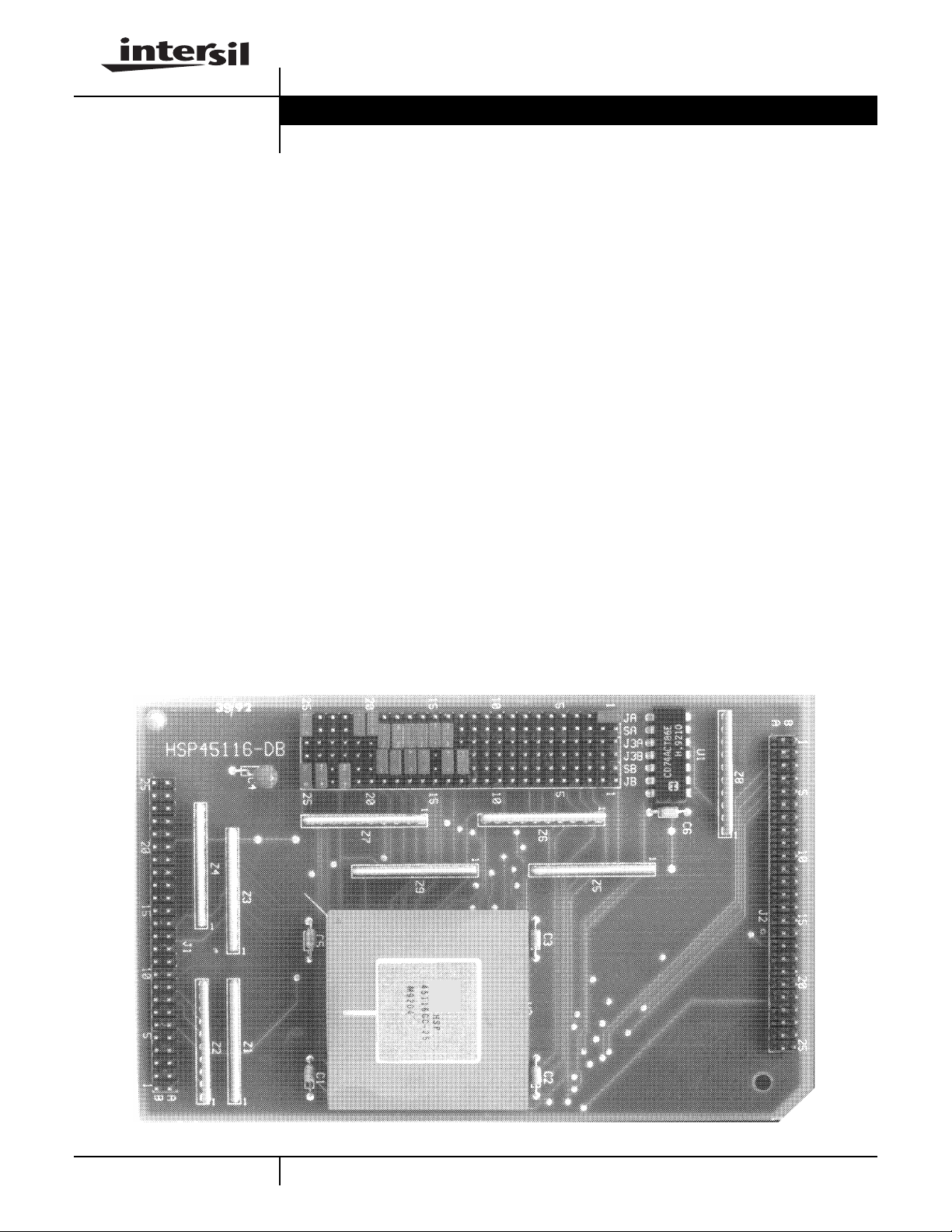
HSP45116-DB
USER’S MANUAL May 1999
HSP45116 Daughter Board
The HSP45116-DB is a daughter board designed to mate
with the HSP-EVAL for rapid evaluation and prototyping of
the HSP45116 Numerically Controlled Oscillator Modulator.
Together, the board set provides a mechanism to evaluate
HSP45116 operation using IBM PC
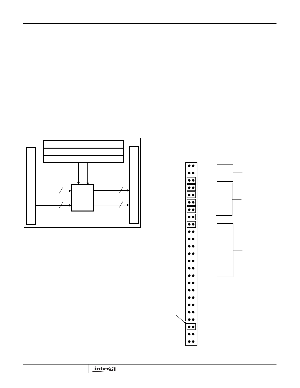
As shown in Figure 1, the HSP45116-DB maps the input,
output, and control signals of the HSP45116 to three 50 pin
headers. These headers mate with connectors on board the
HSP-EVAL to interface the HSP45116’s various I/O and
control signals with the HSP-EVAL’s data busses. This
interface establishes a path for PC
of the HSP45116-DB via the HSP-EVAL.
An IBM PC
controls operation to the HSP45116-DB/HSP-EVAL board
set. The software package provides the user with a DOS
command line interface and graphical user interface for
daughter board I/O and control. Since the software supports
data acquisition from the HSP45116, software based signal
analysis may be used to quantify part performance.
TM
based software package is supplied which
TM
based I/O and control.
TM
based I/O and control
File Number
exert real time control. If a software controlled clock is
provided, the HSP45116-DB can be driven with a user
defined data set, while storing results back to the PC forlater
analysis.
The HSP45116-DB is a 6 layer printed circuit board which
comes populated with one HSP45116GC-25. The PC based
software required to control the daughter board via the
HSP-EVAL is also provided.
3367.3
Features
• Designed for Use with HSP-EVAL
• Access to HSP45116s Input, Output, and Control Signals
Through Three 50 Pin Headers
• HSP45116 Control Signal States May be Set Through
Hardware Configuration or Software
• Two Separate Software Packagesfor Daughter Board I/O
and Control
• High Speed I/O Supported
The degree of control exerted by the software varies
depending upon the clock supplied to the HSP45116-DB. If
a high speed clock is supplied via the HSP-EVAL'son board
oscillator or external clock pin, the software can be used to
HSP45116 Daughter Board
Applications
• PC Based Performance Analysis of HSP45116 When
Used with HSP-EVAL
1
CAUTION: These devices are sensitive to electrostatic discharge; follow proper IC Handling Procedures.
http://www.intersil.com or 407-727-9207
| Copyright © Intersil Corporation 1999
IBM PC™ is trademark of IBM Corporation.
Page 2
HSP45116-DB
Getting Started
This section describes the initial evaluation system setup for
the HSP45116-DB and HSP-EV AL board set. The system
setup consists of mother/daughter board assembly, software
installation, and system test to verify proper operation of the
board set.
Assembly
The evaluation board set is assembled by mating the
HSP45116-DB daughter board with the HSP-EV AL
motherboard. This is accomplished by inserting the header
pins sticking through the bottom (solder side) of the daughter
board into the three 2 x 25 pin connectors on the
motherboard. Proper alignment requires that the J1, J2, and
J3 headers on the HSP45116-DB mate with the J1, J2, and
J3 connectors on the HSP-EVAL. A moderate amount of force
is required to seat the header pins in the motherboard
connectors.
CONFIGURATION JUMPER FIELD A
50 PIN CONTROL HEADER (J2)
CONFIGURATION JUMPER FIELD B
CONTROL
RIN0-15
IMIN0-15
50 PIN INPUT HEADER (J1)
FIGURE 1. HSP45116-DB BLOCK DIAGRAM
16
16
HSP45116
HSP45116-DB
As part of the initial assembly , the HSP-EVAL and HSP45116DB must be provided with the default jumper configuration to
ensure proper operation with the system test software. Each
board leaving the factory is supplied with the default
configuration, but the respective configurations are e xamined
hereforcompleteness. The motherboard'sdefaultconfiguration
is realized by inserting jumpers into the HSP EVAL'sJ4 jumper
field as shown in Figure 2 (see the HSP-EV AL User’s Manual
for more detailed information). The default configuration for the
HSP45116-DB requires jumper placement across the
Configuration Jumper Fields A and B and the J3 Control
Header as shown in Table 1.
Before using the board set with the supplied software, pow er
must be supplied to the boards, and the HSP-EVAL must be
connected to the parallel port of the target PC. Pow er is
provided totheboardsbyconnectingtheV
the J6 header on the HSP-EV AL to a standard 5V±5% supply.
As an alternative, power may be supplied through the HSPEV AL’s 96-Pin DIN connectors. The HSP-EVAL is connected to
the target PC by connecting the HSP-EVAL’s 26-PIN shrouded
header to the PC’s parallel port using the supplied ribbon cable.
CLK
RO0-15
IO0-15
and GND pins of
CC
16
16
50 PIN OUTPUT HEADER (J3)
System Requirements for the Evaluation Board Software
The PC system targeted to run the HSP45116-DB software
(NCOM-SOFT) and interface with the ev aluation board set
must meet the following requirements:
- IBM PC/XT/A T, PS/2, or 100% compatible with a minimum
of 640K of random access memory (RAM) (NCOM-SOFT
does not require extended memory)
- At least 200kB of free disk space on your hard disk
- DOS Version 3.0 or higher
- One parallel port with 27 Pin D-Sub connector
Software Installation
The distribution diskette contains a program called
INSTALL.EXE which installs the NCOM-SOFT software onto
the target hard disk.
you are installing NCOM-SOFT from a diskette in drive A:
onto a hard drive C:. If a different configuration is used,
substitute the letter of the drive where the diskette is
located for drive A;. Substitute the letter for the hard drive
for drive C:
DEFAULT JUMPER
PLACEMENT INDICATOR
FIGURE 2. CONFIGURATION JUMPER FIELD J4
Note: The steps in this section assume
EXT_CLK
OSC_CL
CTL0
OE_BUS1
OE_BUS2
OE_BUS3
OECTLLO
OECTLHI
ADDR0
ADDR1
ADDR2
ADDR3
ADDR4
ADDR5
ADDR6
ADDR7
STAT0
STAT1
STAT2
STAT3
PCRD0
PCRD1
SR_RD
N.C.
N.C.
CLOCK SELECT
JUMPERS
OUTPUT ENABLE
JUMPERS
BOARD ADDRESS
JUMPERS
OUTPUT SELECT
JUMPERS
2
Page 3
HSP45116-DB
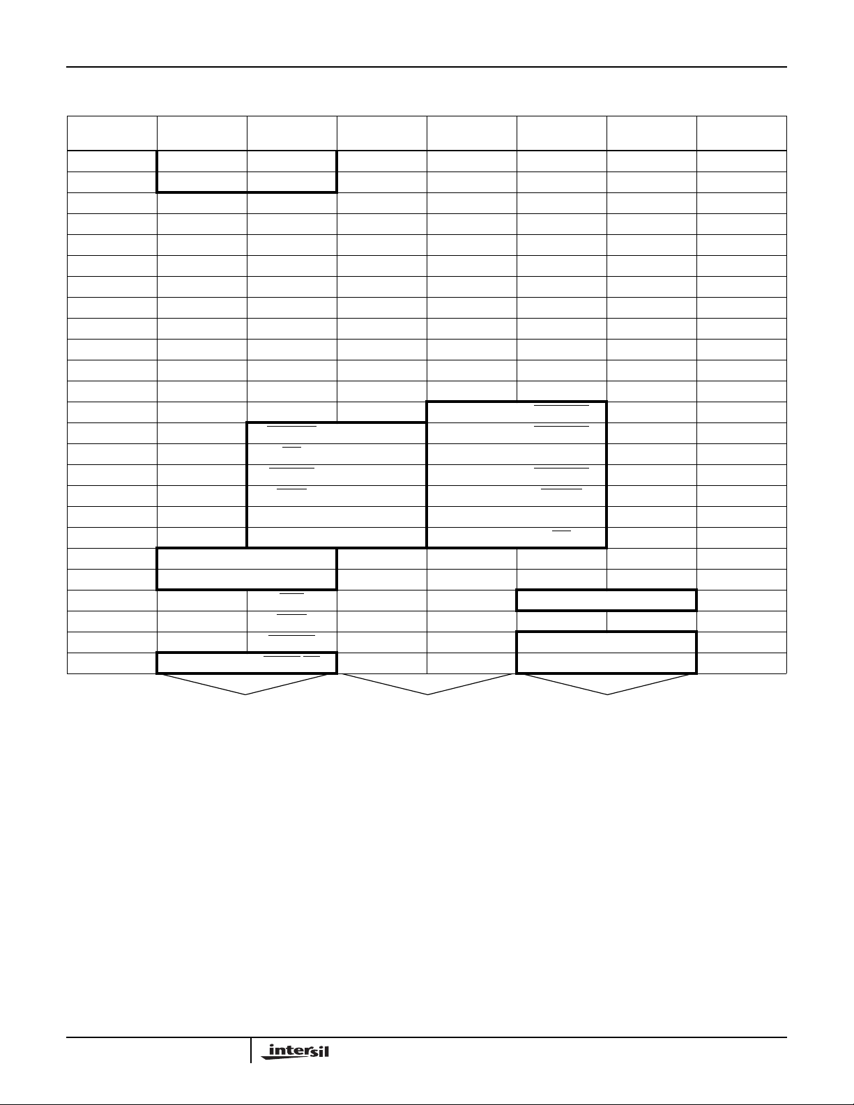
TABLE 1. OVERLAY OF DEFAULT JUMPER CONFIGURATION ONTO THE SIGNAL MAPPING FOR THE J3 CONTROL HEARDER AND
THE CONFIGURATION JUMPER FIELDS A AND B
PIN
NUMBER
1 CLKOUT BUF_IN N.C. GND N.C. GND 1
2 BUF_OUT CLK_IN C0 C1 N.C. GND 2
3 GND PULL UP C2 C3 N.C. GND 3
4 GND PULL UP C4 C5 N.C. GND 4
5 GND N.C. C6 C7 N.C. GND 5
6 GND N.C. GND C8 N.C. GND 6
7 GND N.C. C9 C10 N.C. GND 7
8 GND N.C. C11 C12 N.C. GND 8
9 GND N.C. C13 C14 N.C. GND 9
10 GND N.C. C15 GND N.C. GND 10
11 GND N.C. N.C. N.C. N.C. GND 11
12 GND N.C. CTL1 CT2 N.C. GND 12
13 GND PULL UP CTL3 CTL4 ENPHREG GND 13
14 GND ENTIREG CTL5 CTL6 ENOFREG GND 14
15 GND ENI CTL7 GND N.C. GND 15
16 GND CLROFR CTL8 CTL9 ENCFREG GND 16
17 GND LOAD CTL10 CTL11 BINFMT GND 17
18 GND PMSEL CTL12 CTL13 AD0 GND 18
19 GND AD1 CTL14 CTL15 WR GND 19
20 GND MUX0 GND N.C. N.C. GND 20
21 GND MUX1 GND N.C. N.C. GND 21
22 GND PACI GND N.C. ACC GND 22
23 GND PEAK GND N.C. N.C. GND 23
24 GND RBYTILD GND N.C. MOD0 GND 24
25 GND MODPI/2PI GND N.C. MOD1 GND 25
JA SIGNAL
MNEMONIC
SA SIGNAL
MNEMONIC
J3A SIGNAL
MNEMONIC
J3B SIGNAL
MNEMONIC
SB SIGNAL
MNEMONIC
JB SIGNAL
MNEMONIC
PIN
NUMBER
FIELD A
J3 CONTROL HEADERJUMPER CONFIGURATION
To start the installation program:
Make sure computer is on and the DOS prompt is displayed.
Type: C:<Enter>
Create a subdirectory to contain the NCOM-SOFT Programs
by typing:
MD \NCOMSOFT <Enter>
Change current directory to the NCOMSOFT directory:
CD \NCOMSOFT <Enter>
Start the installation process by typing:
A:INSTALL <Enter>
3
JUMPER CONFIGURATION
FIELD B
The INSTALL program downloads the NCOM-SOFT
programs, NCOMCTRL and NCOM_CMD, to the
NCOMSOFT subdirectory on the target hard drive. In
addition, a subdirectory called NCOM_CHK is created into
which files used to perform functional verification are
downloaded.
Modifications to AUTOEXEC.BAT
To run the NCOM-SOFT programs, DOS must be able to
find the executablefiles.To ensure that DOS can always find
the NCOM-SOFT executables, modify the search path to
include the location of the NCOM-SOFT directory. For
example,iftheNCOM-SOFTprogramsareinstalledondrive
C: in a subdirectory called \NCOMSOFT, add the following
Page 4

HSP45116-DB
line to the end of the existing Path command in the
AUTOEXEC.BAT file:
;C:\NCOMSOFT
If your AUTOEXEC.BAT file does not contain a PATH
command, add the following command to the file:
PATH=C:\NCOMSOFT
Reboot the PC so that the search path changes will take
effect.
System Test
Test software is provided to verify operation of the HSPEVAL and HSP45116-DB board set. Prior to performing the
system test, it is assumed that the evaluation board set has
been assembled and configured as described above; power
has been applied to the board set, and the 26-Pin shrouded
header on board the HSP-EVAL has been connected to the
parallel port of the target PC via the supplied cable. The
system test is initiated by the following:
Change the current directory to that which contains the
software required for the system test by typing
CD C:\NCOMSOFT\NCOM_CHK <Enter>
Run the system test software by typing:
NCOM_CHK <Enter>
The NCOM_CHK.BAT batch file makesuseoftheCommand
Line Interface (see Command Line Interface Section) to
initialize the evaluation board set; clock a data vector
through the HSP45116-DB, and store the output to a file.
The output file is then compared, using the DOS command
COMP, to a file containing a set of vectors generated by a
properly functioning board set. If the files match, the
assembled board set passes operational verification.
the user should answer NO to the COMP command
prompt to compare additional files.
NOTE:
HSP45116-DB Control Panel Software
The HSP45116-DB Control Panel is a graphical user
interface for controlling the operation of the HSPEVAL/HSP45116-DB Board Set via an IBM PC or
compatible. The control panel, as shown in Figure 3,
supports loading the HSP45116's frequency, phase, and
timer accumulator configuration registers, as well as setting
the state of various control inputs. In addition, the control
panel is used to specify files which serve as a data source
fortheHSP45116'sRIN0-15andIMIN0-15inputsanda data
sink for the RO0-15 and IO0-15 outputs. Operation of the
control panel software is dependent on the clock source
provided to the HSP45116-DB as specified in the clock
select portion of the control panel. The HSP45116-DB
Control Panel is invoked by typing:
NCOMCTRL <Enter>
Port Configuration
Communication between the Control Panel software and the
evaluation board set requires that the software kno ws which
of the PC'sparallelports isbeingusedf orcommunication with
the HSP-EV AL and which board address the HSP-EVAL has
been configured for . The default configuration assumes that
LPT1 is being used and the HSP-EV AL has been configured
for a board address of 0. The P ort Configuration can be
inspected by opening up the port configuration window using
the F9 function key. As shown in Figure 4, the window
displays the av ailable parallel ports and their addresses. Also
displayed are the current port and HSP-EVAL Board address
being used by the Control Panel software.
The NCOM_CHK system test assumes that the LPT1 printer
port is being used for communication with the HSP-EVAL. If
another printer port is used, the Command Line Interface,
NCOM_CMD, must be used to configure the software for
using the other port (see NCOM_CMD’s PC and P#
command).
4
Page 5

HSP45116-DB
HSP45116-DB CONTROL PANEL
CLOCK SELECT FILE I/O SELECT
MANUAL CLK
√
PORT CLK
OSC. CLK
EXTERNAL CLKA
CONTROL SIGNALS
0 ENPHREG
0 CLROFR
1
LOAD
1 BINFMT
1 PMSEL
CENTER FREQUENCY REGISTER 40000000
OFFSET FREQUENCY REGISTER 00000000
F1 - HELP F2 - START CLOCK F0 - PORT CONFIG F10 - QUIT
FIGURE 3. CONTROL PANEL SCREEN AS DISPLAYED ON PC
INPUT FILE: INPUT.DAT
√
OUTPUT FILE: OUTPUT.DAT
√
(RINO-15) 7FFF
(IMINO-15) 0000
HSP45116-DB CONTROL PANEL
HSP45116
NCOM
CLOCK NUMBER 0
PHASE OFFSET REGISTER 0000
TIME ACCUMULATOR REGISTER 00000000
0000 (RO0-15)
0000 (IO0-15)
CLOCK SELECT FILE I/O SELECT
MANUAL CLK
PORT CLK
√
OSC. CLK
EXTERNAL CLKA
CONTROL SIGNALS
0 ENPHREG#
0 CLROFR#
1 LOAD #
1 BINFMT#
1 PMSEL
CENTER FR
OFFSET FREQ
F1 - HELP ESC - RETURN F10 - QUIT
AVAILABLE PRINTER PORTS
CURRENT PORT SELECTION : LPT1
CURRENT HSP-EVAL ADDRESS : 0
FIGURE 4. PORT CONFIGURATION WINDOW AS DISPLAYED ON PC
INPUT FILE: 1MHZCMP
OUTPUT FILE: UPCNVRTI
LPT1
LPT2
LPT3
PORT CONFIGURATION
ADDRESS (HEX)
0x3BC
0x378
0x3BC
0-15)
0-15)
000
00000000
5
Page 6

HSP45116-DB
The current port and HSP-EVAL address are changed by
opening up the PortConfigurationWindow, using the up/down
arrow keys to select the desired parameter, and toggling the
space bar to change the selection. Proper operation of the
control panel software requires that the HSP-EVAL Board
address specified in the port configuration window matches
the address jumpered in the Address Selection Section of the
HSP-EV AL’s J4 jumper field (see HSP-EVAL User’s Manual).
Clock Select
The Clock Select portion of the control panel is used to tell
the Control Panel software which of four different clock
sources is being supplied to the HSP45116-DB. The choices
include one of two different software generated clocks
(Manual CLK or Port CLK), an oscillator clock provided by
the HSP-EVAL (OSC. CLK), or an externally supplied clock
(External CLK). The clock mode selected must be consistent
with the Clock Select jumper position in the HSP-EVAL’s J4
jumper field. If either Manual CLK or Port CLK are specified
in the Control Panel, the clock select jumper must be
inserted in the CTL0 position. If either OSC. CLK or External
CLK is specified, the jumper must be inserted at the
OSC_CLK or EXT_CLK position respectively.
In Manual CLK mode, single clock pulses are sent to the
HSP45116 by depressing the F2 function key. The clock
pulse is softwaregeneratedbysettingandclearingtheCTL0
bit of the CTL Control Register on the HSP-EVAL.Aftereach
clock, the HSP45116-DB's RO0-15 and IO0-15 outputs are
serialized and read into the PC for display in the Control
Panel. In this mode, file input and output is supported (see
File I/O Select Section).
In Port CLK mode, a free running clock is sent to the
HSP45116 by depressing the F2 function key. The clock
pulses are software generated by continually setting and
clearing the CTL0 bit of the CTL0-15 Register on the HSPEVAL. After each clock the HSP45116-DB's RO0-15 and
IO0-15 outputs are serialized and read into the PC for
display in the Control Panel. In this mode, file input and
output is supported (See File I/O Select Section).
In OSC. CLK mode, the HSP45116 is supplied with a clock
by the oscillator on-board the HSP-EVAL. In this mode, the
Control Panel can be used for modifying the various control
signal states, the configuration registers, and the complex
inputs to the NCOM. However, the software is unable to
provide file based I/O to the evaluation board set since the
data rate required by the oscillator clock is orders of
magnitude greater than that possible through the parallel
port of the PC. As a result, the Control Panel disables file
based I/O and the display of NCOM output in this mode.
In External CLK mode, the HSP45116 is supplied with a
clock through the 96-Pin DIN connector P1 on the HSPEVAL. In this mode, the Control Panel can be used for
modifying control signal states, the various configuration
registers, and the complex inputs to the NCOM. However,
the softwaredoesnotsupport file based I/O to the evaluation
board set since the data rate required may be much greater
than that capable through the parallel port of the PC. In this
mode, the Control Panel disables file based I/O and the
display of NCOM output.
The clocking mode used by the control panel is indicated by
the position of the “check mark” symbol within the Clock
Select portion of the Control Panel. A different clocking
mode may be selected by positioning the “check mark”
symbol in front of the desired clocking mode. The position of
the “check mark” is changed by using the cursor keys to
move the active window to the desired position and then
toggling the space bar to move the “check mark”.
File I/O Select
The File I/O Select portion of the Control Panel allows the
user to specify files which can be used as an input data
source or an output data sink for the HSP45116-DB. If file
based input is selected, Control Panel software down loads
data from the specified file to registers on the HSP-EVAL
and clocks the data into the RIN0-15 and IMIN0-15 inputs of
the HSP45116. If file based output is specified, the software
reads the data on the RO0-15 and IO0-15 outputs of the
HSP45116 via the HSP-EVAL’s output shift register and
stores the data in the specified file. The input data is loaded
on to the input busses prior to the software generated clock
and the output data is read from the output busses following
the software generated clock.
File based I/O is activated by using the space bar to toggle
the “check mark” symbol in the window proceeding the Input
and Output File identifier in the Control Panel's File I/O
Section. If either file input or output is activated, the
respective file name must be entered in the window to the
right of the I/O file identifier. File input or output may be
disabled at any time by toggling the respective “checkmark”.
Note: file I/O is only valid when either the ‘Manual CLK’
or ‘Port CLK’ clocking modes are selected and it is
disabled if other clocking modes are specified.
The input and output data files are ASCII based and have a
format as described in Appendix A. There is no limitation to
the input and output file size, and care must be taken if file
output is specified since data is collected in the file until file
output is deactivated or the NCOMCTRL Program is exited.
HSP45116 Complex Data Inputs
The data windows to the left of the HSP45116 icon are used
to specify hexadecimalvalues which drivethepart's complex
inputs, RIN0-15 and IMIN0-15. Data entered into these
windows is down loaded to registers on the HSP-EVAL
which drive the HSP45116-DB's complex input busses.
Note: Jumpers must be inserted into the OE_BUS1 and
OE_BUS2 positions of the HSP-EVAL's J4 jumper field
to enable the register outputs containing the complex
data.
6
Page 7

HSP45116-DB
The complex inputs may be changed by entering
hexadecimalvaluesintothedatawindows. The contents of a
particular data window may be edited by depressing the
<Enter> key and using the arrow keys to position the cursor
on the hexadecimal character to be modified.
If file input is selected, the complex inputs are driven with
data from the specified file. On each clock the data windows
are updated with the complex sample down loaded from the
file. In this mode the complex input data windows maynotbe
manually updated.
Control Signals
The Control Signal portion of the control panel is used to
define the state of various control signal inputs to the
HSP45116. The logical state of a control signal is set by
using the space bar to toggle the signal state in the window
preceding the specified control signal. For the control signal
states displayed in the Control Panel to be active at the
HSP45116, the respective control signals must be jumpered
to the HSPEVAL’s CTL0-15 Bus via the HSP45116-DB's J3
jumper field as shown in the default jumper configuration
displayed in Table 1 (see Jumper Configuration Section).
The Control Signal descriptions are contained in the
HSP45116 Data Sheet.
Configuration Registers
The bottom of the control panel displays four data windows
which contain the hexadecimal values loaded into the
HSP45116's Center Frequency, Offset Frequency, Phase
Offset, and Time Accumulator Registers. The contents of a
particular configuration register may be updated by entering
a new hexadecimal value into the data window. The current
value in a window may also be edited by depressing the
<Enter> key and using the arrow keys to position the cursor
on the hexadecimal character to be modified.
terminating an edit by the <Enter> key. If the data window is
associated with the Phase Offset Register, the 16-Bit
hexadecimal value is down loaded into the HSP45116's
Phase Input Register. If the data window is one of the three
32-bit windows associated with the Center Frequency, Offset
Frequency, of TimerAccumulatorRegisters ,the 32-bit value is
loaded into the HSP45116's MS and LS Input Registers and
either
ENCFREG, ENOFREG, or ENTIREG is asserted
respectively. Then, the enable signal is de-asserted and
registered on chip by another software generated clock. In
either Manual or Port Clock modes, a PC generated cloc k is
issued to ensure that the corresponding enable signal is
registered on chip (see HSP45116 Data Sheet). In either of
the other two clock modes, it is assumed that the clock rate is
high enough to register the enable signal before another
Configuration Register is updated. For proper operation, the
register enables,
WR, and A0-1 inputs must be jumpered to
the HSP-EV AL's control bus and inputs via the J3 Control
Header as shown in the Default Jumper Configuration
(Table 1).
Help
Help windows are provided as a source of information for
control panel usage. The help window is activated by the F1
function key, and contains information based on the current
active data window.
Command Line Interface
As an alternative to the control panel, a command line
interface is provided which allows the user to control the
HSP45116-DB by issuing commands from the DOS prompt.
The commands perform basic I/O and configuration
functions by up or down loading data to the HSP45116
through the HSP-EVAL. The Command Line program has
the following usage:
The value entered into the data window is down loaded to the
HSP45116 after leaving the window via the arrow keys or
TABLE 2. COMMAND LIST FOR COMMAND LINE INTERFACE SOFTWARE
COMMAND
CF 32-BIT
HEXADECIMAL VALUE
OF 32-BIT
HEXADECIMAL VALUE
TI 32-BIT
HEXADECIMAL VALUE
PO 16-BIT
HEXADECIMAL VALUE
CL 16-BIT
HEXADECIMAL VALUE
RI 16-BIT
HEXADECIMAL VALUE
II 16-BIT
HEXADECIMAL VALUE
ARGUMENT
#1
ARGUMENT
#2 COMMAND DESCRIPTION
Loads HSP45116’sCenter Frequency Registerwithhexadecimal value specified in
Argument #1. See Notes 1 and 2.
Loads HSP45116’s Offset Frequency Register with hexadecimal valuespecified in
Argument #1. See Notes 1 and 2.
Loads HSP45116’s TimeAccumulatorRegister with hexadecimalvalue specified in
Argument #1. See Notes 1 and 2.
Loads HSP45116’sPhase Input Register withhexadecimal value specified inArgument #1. See Note 2.
Loads the HSP-EVAL’s CTL Control Register with the 16-bit value specified in Argument #1.
Loads thespecifiedHex value intotheHSP-EVALRegister(InputRegister #2) driving the Real Input bus (RIN0-15) Of The HSP45116-DB. See Note 3.
Loads The Specified Hex Value Into The HSP-EVAL Register (Input Register #1)
driving the imaginary Input Bus (IMIN0-15) Of The HSP45116-DB. See Note 3.
7
NCOM_CMD [Command] [ARG 1] [ARG 2]
Page 8

HSP45116-DB
TABLE 2. COMMAND LIST FOR COMMAND LINE INTERFACE SOFTWARE (Continued)
ARGUMENT
COMMAND
PF INPUT FILE OUTPUT
CK Issues softwaregeneratedclock pulse to HSP45116-DBby toggling theCTL0bit in
RD Reads data on the HSP45116-DB’s RO0-15 and IO0-15 outputs and prints data to
SM Displays signal mapping between the CTL Control Register and the HSP45116
CR Displays current state of CTL Control Register.
PC Displays the printer port and HSP-EVAL board address that the NCOM_CMD pro-
P# PORT NUMBER
? List available commands together with a brief description.
NOTES:
1. The CF, OF, TI commands load the specified 32-bit valueintotheHSP45116’sMSandLSinputregisters. After the configuration data has been
loaded into the MSandLSRegisters,the corresponding enable, ENCFREG, ENOFREG, or ENTIREG isasserted.Theenable signal is then registered on chip by a single software generated clock provided a jumper is inserted at the CTL0 position of the J4 jumper field on the HSP-EVAL.
Otherwise, it isassumedthat the selected clock source isfastenough to register the enable signalpriorto a subsequent load of oneofanother 32bit configuration register.Theregister enables, ENCFREG, ENOFREG, andENTIREG must be jumpered to the CTLControlBus as in the default
configuration shown in Table 1.
2. When commands are issued to load registers internal to the HSP45116, it is assumed that the microprocessor interface signals, WR and A0-1
are jumpered to the CTL0-15 bus as in the default configuration shown in Table 1.
3. If the complexinputbusesof the HSP45116-DB are to be driven by the HSP-EVAL’sInputRegisters1 and 2, their outputs must be enabled by
placing jumpers in the OE_BUS1 and OE_BUS2 positions of the J4 jumper field on the HSP-EVAL.
4. Thiscommandis onlyvalidif asoftware generated clocksource has beenselected by insertinga jumper inthe CTL0 positionof theHSP-EVAL’s
J4 jumper field.
5. Commands requiredtoreaddata on the HSP45116-DB’s complex outputs only functionproperlyifthe output of the shift register isselectedfor
reading by inserting a jumper in the SR_RD position of the HSP-EVAL’s J4 jumper field.
#1
(1-3)
ARGUMENT
#2 COMMAND DESCRIPTION
FILE
BOARD
ADDRESS
(0-7)
Down loads complex samples stored in the file specified by Argument #1 into the
HSP-EVAL Registers driving the Real and Imaginary Input Buses of the
HSP45116-DB, clocks the data into the part, and stores the complex output to the
file specified by Argument#2.Theinputandoutputfile formats are specified in Appendix A. See Notes 3, 4 and 5.
the HSP-EVAL’s CTL0-15 Register. See Note 4.
screen. See Note 4 and 5.
control inputs (assumes default jumper configuration shown in Table 1).
gram is using for communication between the PC and the HSP-EVAL. The HSPEVALboard address is set by inserting a jumper in the ADDR0-7 positions of it’s J4
Jumper Field.
Change The Printer Port And HSP-EVAL Board Address that the NCOM_CMD Programisusing forcommunication betweenthePC andtheHSP-EVALto those specified
in Arguments 1 and 2. The HSP-EVAL Board Address is set by inserting a Jumper in
the ADDR0-7 positions of it’s J4 Jumper Field.
The Command specifies 1 of 14 actions to be taken, and the
Arguments (ARG1, ARG2) represent additional data
required by the command. For example, the HSP45116's
Center Frequency Register would be loaded with a value of
40000000(HEX) by typing:
NCOM_CMD CF 40000000 <Enter>
A summary of the command set is contained in Table 2.
Proper operation of the Command Line software is ensured
if the default jumper configurations for the HSP45116-DB
and the HSP-EVAL shown in Table 1 and Figure 2 are used.
However,modifications to this configuration may be required
depending on the clock source and the mode of operation.
The Command Line Interface gives the user the ability to
control the evaluation board set via DOS batch files or
system calls from a programming language. The
NCOM_CHK.BAT file discussed in the System Test Section
8
is an example of how the Command Line program might be
used in a DOS batch file.
Signal Headers
The HSP45116-DB maps the NCOM's inputs and outputs to
three 50-pin signal headers, J1-J3. The signal headers are
used to connect the NCOM’s I/O and control pins to the
HSP-EVAL’s I/O and control busses through three 50
position connectors. The Control Panel and Command Line
interfacesoftwarecontrolthe operation of the HSP45116-DB
by up or down loading data to registers on-board the HSPEVAL which drive or monitor the I/O and control busses.
The J1 Input Header maps two 16-bit busses to the real and
imaginary inputs of the HSP45116, RIN0-15 and IMIN0-15.
In addition, a bidirectional clock line is routed to this header
as shown by the signal map in Table3.Whenmated with the
J1 connector on the HSP-EVAL, the HSP45116's real and
imaginary inputs map to the HSP-EVAL's Input Bus 2 and 1,
IN2_0-15 and IN1_0-15, respectively.
Page 9

HSP45116-DB
TABLE 3. SIGNALASSIGNMENTSFOR 50 POSITION INPUT
CONNECTOR J1
PIN
NUMBER
1 N.C. GND
2 RIN0 RIN1
3 RIN2 RIN3
4 RIN4 RIN5
5 RIN6 RIN7
6 GND RIN8
7 RIN9 RIN10
8 RIN11 RIN12
9 RIN134 RIN14
10 RIN15 GND
11 N.C. IMIN0
12 IMIN1 IMIN2
13 IMIN3 IMIN4
14 IMIN5 IMIN6
15 IMIN7 GND
16 IMIN8 IMIN9
17 IMIN10 IMIN11
18 IMIN12 IMIN13
19 IMIN14 IMIN15
20 GND CLKIN
21 GND N.C.
22 GND V
23 GND V
24 GND V
25 GND V
J1A SIGNAL
MNEMONIC
J1B SIGNAL
MNEMONIC
CC
CC
CC
CC
TABLE 4. SIGNAL ASSIGNMENTS FOR 50 POSITION OUT-
PUT CONNECTOR J2
PIN
NUMBER
1 OER GND
2 RO0 RO1
3 RO2 RO3
4 RO4 RO5
5 RO6 RO7
6 GND RO8
7 RO9 RO10
8 RO11 RO12
9 RO13 RO14
10 RO15 GND
11 OEI IO0
12 IO1 IO2
13 IO3 IO4
14 IO5 IO6
15 IO7 GND
16 IO8 IO9
17 IO10 IO11
18 IO12 IO13
19 IO14 IO15
20 GND CLKOUT
21 GND TICO
22 GND PACO
23 GND N.C.
24 GND N.C.
25 GND N.C.
J2A SIGNAL
MNEMONIC
J2B SIGNAL
MNEMONIC
The J2 Output Header maps two 16-bit busses to the real
and imaginary outputs of the HSP45116, RO0-15 and IO0-
15. In addition, two HSP45116 status outputs,
PACO and
TICO, two HSP45116 output enables, OER and OE, and a
bidirectional clock line are routed to this header as shown by
the signal map in Table 4. When mated with the J2
connector on the HSP-EVAL, the HSP45116's real and
imaginary outputs map to the HSP-EVAL'sOutputBus2and
1, OUT2_0-15 and OUT1_0-15, respectively.
The J3 Control Header maps one 16-bit bus to the
HSP45116's control input, C0-15, and provides jumper
positions for the Configuration Jumper Fields that flank the
header. When mated with the HSP-EVAL's J3 Control
Connector the HSP45116's Control Inputs, C0-15, are
mapped to the HSP-EVAL's Input Bus 3, IN3_0-15, and the
jumper positions are mapped the HSP-EVAL's Control Bus,
CTL0-15. The signal map fortheJ3ControlHeaderisshown
in Table 1.
9
Configuration Jumper Field
The Configuration Jumper Fields A and B flank either side of
the Control Header J3 as shown in Table 1. Positions within
the Jumper Field's SA and SB signal rows map to various
HSP45116 control inputs. The control inputs may be
jumpered to ground or the HSP-EVAL'sCTL4-15 bus via the
J3 Control Header. If a control signal mapped to SA and SB
is not jumpered to GND or CTL4-15, the signal is pulled
high.
The Configuration Jumper Field A is also used to select
whether the HSP45116's clock source is provided through
the J1 Input Header or the J2 Output Header. If jumpers are
inserted as shown in Figure 5, a clock signal supplied
through the CLK_IN pin of the J1 Input Header drives a
buffer whose output clocks the HSP45116. The jumper
inserted between JA1 and JA2 feeds the buffered clock
signal to the CLK_OUT pin of the J2 Output Header. If
jumpers are inserted as shown in Figure 6, the CLK_OUT
pin of the J2 Output Connector drives the clock buffer which
Page 10

HSP45116-DB
in turn drives the clock input of the HSP45116. The jumper
inserted between JA2 and SA2 allows the Input Header’s
CLK_IN pin to be driven by the buffer output.
NOTE: The
jumper placement shown in Figure 5 is the standard
configuration.
FIGURE 5. JUMPER CONFIGURATION IF CLOCK IS SUP-
FIGURE 6. JUMPER CONFIGURATION IF CLOCK IS SUP-
.
JASAJ3A
1
PLIED THROUGH J1 INPUT HEADER
JASAJ3A
1
PLIED THROUGH J2 OUTPUT HEADER
The HSP45116-DB is shipped from the factory with the
default jumper configuration shown by the overlay of heavy
lines onto the signal map in Table 1. For the Control Panel
and Command Line Interface software to properly control
operation of the HSP45116, it is assumed that the
HSP45116 control inputs are jumpered as specified in the
default configuration. Also, the system test software,
NCOM_CHK, must be run using the default configuration.
Appendix A
Data File Structures
The Input/Output data files used by the HSP45116-DB
Control PanelandCommand Line Interfacesoftwarecontain
complex data samples. The data files consist of a seven line
header followed by the data itself. The header section must
follow this format:
Line 1: Comment #1
Line 2: Comment #2
Line 3: Comment #3
Line 4: Comment #4
Line 5: Comment #6
Line 7: c 1 n
(Real Component) (Imaginary Component)
•
•
•
The ‘n’ on the 7th line of the header should be replaced by
the number of complex samples in the file. Following the
header,the complex samples are listed one per row with the
real part listed first followed by the complex part. The real
and imaginary components of the complex data sample are
represented as 16-bit two’s complement values. As a result,
the real and imaginary parts of the data sample are integer
values bounded by 32767 and -32768. The CMPRFILE
installed in the NCOM_CHK subdirectory is an example of
the input data file structure.
10
Page 11

HSP45116-DB
VCC
C5
0.01µF
C1
0.01µF
C2
0.01µF
C3
0.01µF
OER
OEI
12345678910111213141516171819202122232425
J2B
RO1
RO3
RO5
RO7
RO8
RO10
RO12
RO0
RO2
RO4
RO6
RO9
RO11
123456789
J2A
C4
0.01µF
IO4
IO3
IO6
IO5
IO7
IO9
IO8
IO11
IO10
IO13
IO12
IO15
IO14
RO14
IO0
IO2
RO13
RO15
IO1
101112131415161718192021222324
CKOUT
25
RIN[0..15]
IMIN[0..15]
ENCFREG
ENOFREG
VCC
GND
VCC
C[0..15]
NCOMCK
123456789
SB
12345678910111213141516171819202122232425
JB
12345678910111213141516171819202122232425
J3B
C10
C1C3C5C7C8
C0C2C4
123456789
J3A
C12
C6
C9
C11
ENPHREG
101112131415161718192021222324
CTL0
CTL2
CTL4
CTL6
CTL9
C14
C13
C15
CTL5
CTL7
CTL8
CTL3
CTL1
101112131415161718192021222324
AD0
BINFMT
CTL11
CTL13
CTL10
CTL12
WR
CTL15
CTL14
ACC
MOD0
MOD1
Z9
7 2 3 4 5 6 8 9 0
1
25
25
VCC
U1D
1
11
74AC86
12345678910111213141516171819202122232425
J1B
VCC
RIN1
RIN3
RIN5
RIN0
RIN2
RIN4
123456789
J1A
TICO
PACO
RIN7
RIN6
RIN8
RIN10
RIN12
RIN14
IMIN0
RIN9
RIN11
RIN13
RIN15
101112131415161718192021222324
IMIN4
IMIN2
IMIN1
IMIN3
IMIN6
IMIN5
IMIN7
IMIN9
IMIN11
IMIN10
IMIN8
IMIN13
IMIN12
CKIN
IMIN15
IMIN14
12345678910111213141516171819202122232425
JA
CKOUT
12345678910111213141516171819202122232425
SA
CKIN
3
6
74AC86
U1A
25
IO[0..15]
RO[0..15]
U1B
1
2
4
5
74AC86
9
U1C
8
10
74AC86
ENTIREG
ENI
CLROFR
LOAD
AD1
MUX0
PMSEL
PACI
MUX1
PEAK
RBYTILD
MODPI/2PI
13
12
VCC
1
Z8
2
3 4 5 6 7 8 9 0
1
2 3 4 5 6 7 8 9 0
1
Z7
1
VCC
11
Page 12

RO[0..15]
HSP45116-DB
PACO
IO[0..15]
TICO
VCC
GND
RO0
RO1
RO2
RO3
RO4
RO5
RO6
RO7
RO8
RO9
RO10
RO11
RO12
RO13
RO14
RO15
K13
L15
J13
H14
G15
F15
G14
F14
F13
E15
E14
RO0 M15
RO1
RO2 K14
RO3
RO4 J14
RO5
RO6 K15
RO7
RO8 H13
RO9 G13
RO10
RO11
RO12
RO13
RO14
RO15
RIN0
RIN1
RIN2
RIN3
RIN4
RIN5
RIN6
RIN7
RIN8
RIN9
RIN10
RIN11
RIN12
RIN13
RIN14
RIN15
RIN16
K2J2K1J1J3H3H2F1G3G2E1F2F3D1E2C1E3D2C2D3B2C3C4A2B3C5B4A3A4B5A5C6B6B7A6A7C7
RIN0
RIN1
RIN2
RIN3
RIN4
RIN5
RIN6
RIN7
RIN8
RIN9
RIN10
RIN11
RIN12
RIN13
RIN14
RIN15
RO16
D15
C15
RO17
RO18
RIN17
RIN18
D14
RO19
U2
IMIN0
IMIN0
IO0
IO1
IO2
IO3
IO0 E13
IO1 C14
IO2 B15
IO3 D13
HSP45116
IMIN1
IMIN2
IMIN3
IMIN4
IMIN1
IMIN2
IMIN3
IMIN4
IO4
IO5
B14
IO4 C13
IO5
IMIN5
IMIN6
IMIN5
IMIN6
IO6
IO7
B13
IO6 C12
IO7
IMIN7
IMIN8
IMIN7
IMIN8
IO8
IO9
C11
IO8 B12
IO9
IMIN9
IMIN10
IMIN9
IMIN10
IO10
IO11
A13
B11
IO10
IO11
IMIN11
IMIN12
IMIN11
IMIN12
IO12
IO13
A12
C10
IO12
IO13
IMIN13
IMIN14
IMIN14
IMIN13
IO14
IO15
B10
A11
IO14
IO15
IMIN15
IMIN16
IMIN15
IMIN17
A10
B8
IO16B9IO17C9IO18
IO19
PACO L13
TICO P1
IMIN18
C0Q14
C1
C3P12
C4Q13
C8
P13C2N11
C0C1C2C3C4C5C6C7C8C9C10
C5Q12
DET0 N15
C6P11
L14
DET1
C7Q11
C8N10
C9P10
N14
M
1
M13
P14
M
2
N
2
L
2
K
3
L
1
P
2
L
3
P
3
N
4
P
4
N
6
Q
4
P
5
Q
3
N
5
1
MN
1
P
6
GND
4
VCC
OEIEX
T
OEI
OEREX
T
OER
PEA
K
BINFM
T
ACC
SH1
SH0
PAC
I
RBYTILD
PMSEL
LOA
D
CLROF
MODPI/2PI
C10P9
C11Q10
C12Q9
C13N9
C14N8
C15P8
ADR0N7ADR1P7CLKQ5WR
C11
C12
C13
C14
C15
ENI
ENTIREG
ENPHA
ENCFREG
ENOFREG
ENPHREG
C
OUTMUX0
MOD0N3MOD1
N13
Q6
M3
R
C
S
OUTMUX1
N12
Z2
2 1
3
4
5
6
7
8
9
10
RIN8
RIN9
RIN10
RIN11
RIN12
RIN13
RIN14
RIN15
Z1
2 1
3
4
5
6
7
8
9
10
RIN0
RIN1
RIN2
RIN3
RIN4
RIN5
RIN6
RIN7
Z4
2 1 3
IMIN8
IMIN9
Z3
2 1 3
IMIN0
IMIN1
RIN[0..15]
4
5
IMIN10
IMIN11
4
5
IMIN2
IMIN3
6
7
IMIN12
IMIN13
6
7
IMIN4
IMIN5
8
9
10
IMIN14
IMIN15
8
9
10
IMIN6
IMIN7
Z6
2 1
3
CIN8
CIN9
Z5
2 1
3
CIN0
CIN1
IMIN[0..15]
4
5
CIN10
CIN11
4
5
CIN2
CIN3
6
7
CIN12
CIN13
6
7
CIN4
CIN5
8
9
CIN14
CIN15
8
9
CIN6
CIN7
10
10
AD0
C[0..15]
AD1
NCOMCK
WR
MOD0
MOD1
MUX1
MUX0
ENCFREG
ENPHREG
ENOFREG
ENI
ENTIREG
MODPI/2PI
CLROFR
LOAD
PMSEL
RBYTILD
PEAK
BINFMT
OER
OEI
ACC
PACI
12
Page 13

HSP45116-DB
HSP-EVAL Limited Warranty
Intersil warrants the HSP-EVAL to be free of defects in
material and workmanship under normal use for a period of
ninety (90) days. Intersil also warrants that the HSP-EVAL
User's Manual is substantially complete and contains all the
information which Intersil considers necessary to use the
HSP-EVAL, and that the HSP-EVAL functions substantially
as described in the HSP-EVAL User's Manual. Intersil will
replace the HSP-EVAL as Intersil's sole duty under this
warranty only if you ship it, postage prepaid, to Intersil within
ninety (90) days of such acquisition and provide proof of
date of acquisition.
This limited warranty does not extend to any products which
have been damaged as a result of accident, misuse, abuse,
or as a result of service or modification by anyone other than
Intersil or Intersil's authorized representatives.
Intersil makes no other express or implied warranty with
respect to the HSP-EVAL other than the limited warranty set
forth above. Intersil disclaims all implied warranties of
merchantability and/or fitness foraparticularpurpose.Inany
event,allimpliedwarranties shall be limited tothedurationof
this warranty. The liability of Intersil, if any, shall under
any tort, contract or other legal theory be limited to the
actual price paid for such product and shall in no event
include incidental, consequential, special or indirect
damages of any kind, even if Intersil is aware of the
possibility of such damages.
HSP45116-DB Software License
Agreement
In return for the purchase price of the HSP45116-DB
product, the Purchaser receives from Intersil Corporation
(“Intersil”) a non-exclusive nontransferable (except as set for
below) license under Intersil copyrights to use the software
subject to the following terms and conditions:
[1] The Software is protected by both United States
Copyright Law and International Treaty provisions.
Therefore, you must treat the Software like any other
copyrighted material (e.g. a book) and may not copy,
distribute or make derivatives of any part thereof except
that you may either a) make one copy of the Software
solely for archival purposes, or b) transfer the Software
to a single hard disk provided you keep the original
solely for backup or archival purposes.
[2] The Software may be transferred to a third party on a
permanent basis provided you retain no copies and the
recipient agrees,inwriting to Intersil, to the terms of this
Agreement.
[3] If the software package contains both 3.5" and 5.25"
disks, then you may use only the disks appropriate for
your single-user computer. You may not use the other
disks on another computer or loan, rent, lease, or
transfer them to another user except as part of the
permanent transfer (as provided above) of all Software.
Intersil reserves the right to revise and make changes to this
manual and the HSP-EVAL from time to time without
obligation to notify any person of, or to provide any person
with, such revisions or changes.
All Intersil semiconductor products are manufactured, assembled and tested under ISO9000 quality systems certification.
Intersil semiconductor products are sold bydescriptiononly. Intersil Corporation reserves the right to make changes incircuitdesign and/or specifications at any time without notice. Accordingly , the reader is cautioned to verify that data sheets are current before placing orders. Information furnished by Intersil is believed to be accurate and
reliable. However, no responsibility is assumed by Intersil or its subsidiaries for its use; nor for any infringements of patents or other rights of third parties which may result
from its use. No license is granted by implication or otherwise under any patent or patent rights of Intersil or its subsidiaries.
For information regarding Intersil Corporation and its products, see web site http://www.intersil.com
Sales Office Headquarters
NORTH AMERICA
Intersil Corporation
P. O. Box 883, Mail Stop 53-204
Melbourne, FL 32902
TEL: (407) 724-7000
FAX: (407) 724-7240
EUROPE
Intersil SA
Mercure Center
100, Rue de la Fusee
1130 Brussels, Belgium
TEL: (32) 2.724.2111
FAX: (32) 2.724.22.05
ASIA
Intersil (Taiwan) Ltd.
7F-6, No. 101 Fu Hsing North Road
Taipei, Taiwan
Republic of China
TEL: (886) 2 2716 9310
FAX: (886) 2 2715 3029
13
 Loading...