

Page 1
HSP45106/883
Data Sheet May 1999
16-Bit Numerically Controlled Oscillator
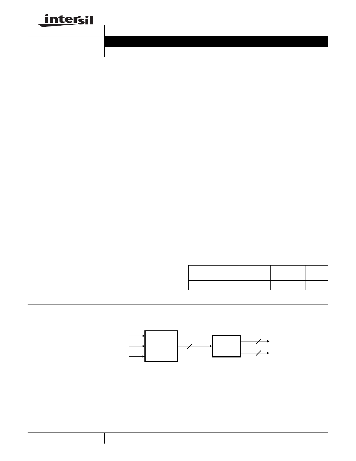
The Intersil HSP45106/883 is a high performance 16-bit
quadrature Numerically Controlled Oscillator (NCO16). The
NCO16 simplifies applications requiring frequency and
phase agility such as frequency-hopped modems, PSK
modems, spread spectrum communications, and precision
signal generators. As shown in the Block Diagram, the
HSP45106/883 is divided into a Phase/Frequency Control
Section (PFCS) and a Sine/Cosine Section.
The inputs to the Phase/Frequency Control Section consist
of a microprocessor interface and individual control lines.
The frequency resolution is 32 bits, which provides for
resolution of better than 0.006Hz at 25.6MHz. User
programmable center frequency and offset frequency
registers give the user the capability to perform phase
coherent switching between two sinusoids of different
frequencies. Further, a programmable phase control register
allows forphasecontrolofbetterthan0.006o. Inapplications
requiring up to 8 level PSK, three discrete inputs are
provided to simplify implementation.
The output of the PFCS is a 32-bit phase argument which is
input to the Sine/Cosine Section for conversion into
sinusoidal amplitude. The outputs of the Sine/Cosine
Section are two 16-bit quadrature signals. The spurious free
dynamic range of this complex vector is greater than 90dBc.
File Number
2815.3
Features
• This Circuit is Processed in Accordance to MIL-STD-883
and is Fully Conformant Under the Provisions of
Paragraph 1.2.1.
• 25.6MHz Clock Rate
• 32-Bit Center and Offset Frequency Control
• 16-Bit Phase Control
• 8 Level PSK Supported Through Three Pin Interface
• Simultaneous 16-Bit Sine and Cosine Outputs
• Output in Two’s Complement or Offset Binary
• <0.006Hz Tuning Resolution at 25.6MHz
• Serial or Parallel Outputs
• Spurious Frequency Components < -90dBc
• 16-Bit Microprocessor Compatible Control Interface
Applications
• Direct Digital Synthesis
• Quadrature Signal Generation
• Modulation - FM, FSK, PSK (BPSK, QPSK, 8PSK)
• Precision Signal Generation
For added flexibility when using the NCO16 in conjunction
with DAC’s, a choice of either parallel of serial outputs with
either two’s complement or offset binary encoding is
provided. In addition, a synchronization signal is available
which signals serial word boundaries.
Block Diagram
MICROPROCESSOR
INTERFACE
CONTROL SIGNALS
DISCRETE
CLOCK
PHASE/
FREQUENCY
CONTROL
SECTION
Ordering Information
TEMP.
PART NUMBER
HSP45106GM-25/883 -55 to 125 85 Ld PGA G85.A
SIN/COS
ARGUMENT
32
SINE/
COSINE
SECTION
RANGE (oC) PACKAGE
SINE
COSINE
16
16
PKG.
NO.
1
CAUTION: These devices are sensitive to electrostatic discharge; follow proper IC Handling Procedures.
http://www.intersil.com or 407-727-9207
| Copyright © Intersil Corporation 1999
Page 2
HSP45106/883
Absolute Maximum Ratings Thermal Information
Supply Voltage . . . . . . . . . . . . . . . . . . . . . . . . . . . . . . . . . . . . +8.0V
Input, Output Voltage Applied . . . . . . . . . .GND -0.5V to VCC +0.5V
ESD Classification . . . . . . . . . . . . . . . . . . . . . . . . . . . . . . . . .Class 1
Operating Conditions
Temperature Range. . . . . . . . . . . . . . . . . . . . . . . . . -55oC to 125oC
Voltage Range. . . . . . . . . . . . . . . . . . . . . . . . . . . . . +4.5V to +5.5V
CAUTION: Stresses above those listed in “Absolute Maximum Ratings” may cause permanent damage to the device. This is a stress only rating and operationofthe
device at these or any other conditions above those indicated in the operational sections of this specification is not implied.
NOTE:
1. θJA is measured with the component mounted on an evaluation PC board in free air.
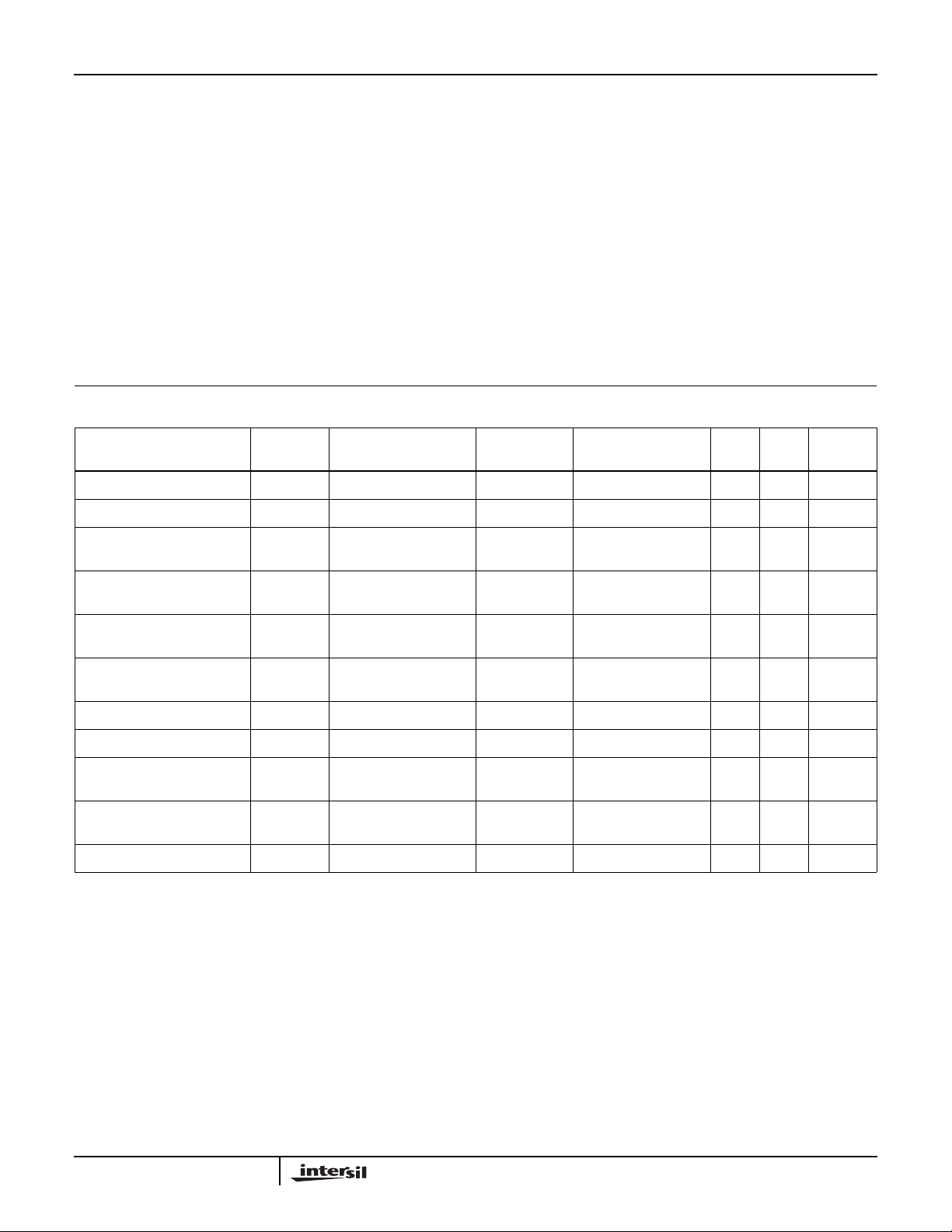
TABLE 1. DC ELECTRICAL PERFORMANCE SPECIFICATIONS
Device Guaranteed and 100% Tested
PARAMETER SYMBOL TEST CONDITIONS
Thermal Resistance (Typical, Note 1) θJA (oC/W) θJC (oC/W)
PGA Package. . . . . . . . . . . . . . . . . . . . 36.0 7.0
Maximum Package Power Dissipation at 125oC
PGA Package. . . . . . . . . . . . . . . . . . . . . . . . . . . . . . . . . . . 1.39W
Maximum Junction Temperature . . . . . . . . . . . . . . . . . . . . . . . 175oC
Maximum Storage Temperature Range . . . . . . . . . . -65oC to 150oC
Maximum Lead Temperature (Soldering 10s) . . . . . . . . . . . . 300oC
Die Characteristics
Gate Count. . . . . . . . . . . . . . . . . . . . . . . . . . . . . . . . . . . . . . . 18,750
GROUP A
SUBGROUPS
TEMPERATURE
(oC) MIN MAX UNITS
Logical One Input Voltage V
Logical Zero Input Voltage V
Output HlGH Voltage V
OH
VCC = 5.5V 1, 2, 3 55 ≤ TA≤ +125 2.2 - V
lH
VCC = 4.5V 1, 2, 3 55 ≤ TA≤ +125 - 0.8 V
IL
IOH = -400µA
1, 2, 3 55 ≤ TA≤ +125 2.6 - V
VCC= 4.5V (Note 2)
Output LOW Voltage V
OL
IOL = +2.0mA
1, 2, 3 55 ≤ TA≤ +125 - 0.4 V
VCC= 4.5V (Note 2)
Input Leakage Current I
VIN = VCCor GND
I
1, 2, 3 55 ≤ TA≤ +125 -10 +10 µA
VCC= 5.5V
Output Leakage Current I
V
O
= VCC or GND
OUT
1, 2, 3 55 ≤ TA≤ +125 -10 +10 µA
VCC= 5.5V
Clock lnput High V
Clock Input Low V
Standby Power Supply
I
Current
Operating Power Supply Cur-
I
rent
IHC
ILC
CCSB
CCOP
VCC = 5.5V 1, 2, 3 55 ≤ TA≤ +125 3.0 - V
VCC = 4.5V 1, 2, 3 55 ≤ TA≤ +125 - 0.8 V
VIN = VCCor GND
1, 2, 3 55 ≤ TA≤ +125 - 500 µA
VCC= 5.5V, (Note 5)
f = 25.6MHz
1, 2, 3 55 ≤ TA≤ +125 - 205 mA
VCC= 5.5V (Notes 3, 5)
Functional Test FT (Note 4) 7, 8 55 ≤ TA≤ +125 - - -
NOTES:
2. Interchanging of force and sense conditions is permitted.
3. Operating supply current is proportional to frequency, typical rating is 8mA/MHz.
4. Tested as follows: f = 1MHz, VIH = 2.6, VIL = 0.4, VOH≥ 1.5V, VOL≤ 1.5V, V
= 3.4V, and V
IHC
ILC
= 0.4V.
5. Loading is as specified in the test load circuit with CL = 40pF.
2
Page 3

TABLE 2. AC ELECTRICAL PERFORMANCE SPECIFICATIONS
PARAMETER SYMBOL NOTES
HSP45106/883
GROUP A
SUBGROUP
TEMPERATURE
(oC)
-25 (25.6MHz)
UNITSMIN MAX
CLK Period t
CLK High t
CLK Low t
WR Period t
WR High t
WR Low t
Setup Time A(2:0), CS to WR
Going High
Hold Time A(2:0), CSfromWR Go-
ing High
Setup Time C(15:0) to WR
Going High
Hold Time C(15:0) from WR
Going High
Setup Time WR High to CLK High t
Setup Time MOD(2:0) to CLK
Going High
Hold Time MOD(2:0)from CLK Go-
ing High
CP
CH
CL
WP
WH
WL
t
AWS
t
AWH
t
CWS
t
CWH
WC
t
MCS
t
MCH
9, 10, 11 -55 ≤ TA≤ 125 39 - ns
9, 10, 11 -55 ≤ TA≤ 125 15 - ns
9, 10, 11 -55 ≤ TA≤ 125 15 - ns
9, 10, 11 -55 ≤ TA≤ 125 39 - ns
9, 10, 11 -55 ≤ TA≤ 125 15 - ns
9, 10, 11 -55 ≤ TA≤ 125 15 - ns
9, 10, 11 -55 ≤ TA≤ 125 13 - ns
9, 10, 11 -55 ≤ TA≤ 125 2 - ns
9, 10, 11 -55 ≤ TA≤ 125 15 - ns
9, 10, 11 -55 ≤ TA≤ 125 1 - ns
Note 8 9, 10, 11 -55 ≤ TA≤ 125 16 - ns
9, 10, 11 -55 ≤ TA≤ 125 15 - ns
9, 10, 11 -55 ≤ TA≤ 125 1 - ns
Setup Time ENPOREG,
t
ECS
9, 10, 11 -55 ≤ TA≤ 125 12 - ns
ENOFREG, ENCFREG,
ENPHAC, ENTIREG, INHOFR,
PMSEL, INITPAC, BINFMT,TEST,
PAR/SER, PACI, INITTAC to CLK
Going High
Setup Time ENPOREG,
t
ECH
9, 10, 11 -55 ≤ TA≤ 125 1 - ns
ENOFREG, ENCFREG,
ENPHAC, ENTIREG, INHOFR,
PMSEL, INITPAC, BINFMT,TEST,
PAR/SER, PACI, INITTAC from
CLK Going High
CLK to Output Delay SIN(15:0),
t
DO
9, 10, 11 -55 ≤ TA≤ 125 - 18 ns
COS(15:0), TICO
CLK to Output Delay DACSTRB t
Output Enable Time t
DSO
OE
Note 7 9, 10, 11 -55 ≤ TA≤ 125 - 12 ns
9, 10, 11 -55 ≤ TA≤ 125 2 18 ns
NOTES:
6. AC Testing: VCC= 4.5V and 5.5V. Inputs are driven at 3.0V for Logic “1” and 0.0V for a Logic “0”. Input and output timing measurements are
made at1.5V for both aLogic “1” and0”.CLK is drivenat4.0V and 0Vand measured at 2.0V.Output load per testload circuit with switchclosed
and CL = 40pF.
7. Transition is measured at ±200mV from steady state voltage with loading as specified by test load circuit and CL = 40pF.
8. IfENOFRCTL, ENCFRACTL,ENTICTL, or ENPHREGare active, caremust be takento not violatesetup andholdtimes tothese registers when
writing data into the chip via the C(15:0) port.
3
Page 4

HSP45106/883
TABLE 3. ELECTRICAL PERFORMANCE CHARACTERISTICS
PARAMETER SYMBOL CONDITIONS NOTES
Input Capacitance
C
IN VCC= Open, f = 1MHz, all measure-
ments are referenced to device GND.
TEMPERATURE
(oC)
9T
= 25 - 10 pF
A
-25 (25MHz)
UNITSMIN MAX
Output Capacitance C
OUT
VCC= Open, f = 1MHz, all measure-
9T
= 25 - 10 pF
A
ments are referenced to device GND.
Output Disable Delay t
Output Rise Time t
Output Fall Time t
OEZ
OR
OF
From 0.8V to 2.0V 9, 10 -55 ≤ TA≤ 125 - 8 ns
From 20.V to 0.8V 9, 10 -55 ≤ TA≤ 125 - 8 ns
9, 10 -55 ≤ TA≤ 125 - 15 ns
NOTES:
9. Parameters listed in Table 3 are controlled via design or process parameters and are not directly tested. These parameters are characterized
upon initial design and after major process and/or design changes.
10. Loading is as specified in the test load circuit with switch closed and CL= 40pF.
TABLE 4. ELECTRICAL TEST REQUIREMENTS
CONFORMANCE GROUPS METHOD SUBGROUPS
Initial Test 100%/5004 Interim Test 100%/5004 PDA 100% 1
Final Test 100% 2, 3, 8A, 8B, 10, 11
Group A - 1, 2, 3, 7, 8A, 8B, 9, 10, 11
Groups C and D Samples/5005 1, 7, 9
4
Page 5

Burn-In Circuit
HSP45106/883
HSP45106/833 (PGA)
1011 59876 4321
L
GND
SIN1 SIN3 SIN5 SIN4 SIN9 SIN12
SIN0 SIN13 SIN14
DAC
STRB
L
V
FMT SIN15
ENP
HAC
ENTI INITT
REG AC
REG REG REG
V
CC
PGA
PIN
CLK SIN2 V
CC
PAR/
SEL
PACI
INHOF
R
WRGNDCS COS11 COS9
TEST COS12GND
MOD0 C10 C6 COS15 COS13
PIN
NAME
BURN-IN
SIGNAL
SIN8 SIN10 GND COSO
CC
SIN6 SIN7 SIN11 OEC COS1
COS7 V
PIN
INDEX
PIN
BURN-IN
SIGNAL
C9
C13 V
PGA
PIN
CC
C7
NAME
OES
COS2 COS3
COS5COS6 COS4
COS8
COS10
TICOC1C4
CC
C0
PGA
PIN
K
J
H
G
F
E
D
C
B
A
PIN “A1”
PIN
NAME
PGA
PIN
PIN
NAME
K
J
INIPAC
H
G
ENCF ENPO ENOF
F
E
D
C
MOD2
B
MOD1 A2 A1 C15 C12 COS14
A
PMSEL A0 GND C14 C11 C8 C5 C3 C2
BURN-IN
SIGNAL
A1 C0 F7 B11 MOD1 F13 F9 ENOFREG F8 K2 OES F14
A2 C2 F7 C1 COS13 VCC/2 F10 ENPOREG F4 K3 SIN15 VCC/2
A3 C3 F7 C2 COS15 VCC/2 F11 ENCFREQ F7 K4 GND GND
A4 C5 F8 C5 C6 F8 G1 COS5 VCC/2 K5 SIN10 VCC/2
A5 C7 F8 C6 C9 F10 G2 COS4 VCC/2 K6 SIN8 VCC/2
A6 C8 F10 C7 C10 F10 G3 COS6 VCC/2 K7 V
CC
A7 C11 F10 C10 MOD0 F12 G9 INHOFR F11 K8 SIN2 VCC/2
A8 C14 F11 C11 MOD2 F14 G10 INITTAC F13 K9 CLK F0
A9 GND GND D1 COS12 VCC/2 G11 ENTIREG F12 K10 V
CC
A10 A0 F8 D2 GND GND H1 COS3 VCC/2 K11 BINFMT F6
A11 PMSEL F14 D10 TEST F14 H2 COS2 VCC/2 L1 DACSTRB VCC/2
B1 COS14 VCC/2 D11 V
CC
V
CC
H10 PACI F11 L2 SIN14 VCC/2
B2 TICO VCC/2 E1 COS9 VCC/2 H11 ENPHAC F10 L3 SIN13 VCC/2
B3 C1 F7 E2 COS10 VCC/2 J1 COS1 VCC/2 L4 SIN12 VCC/2
B4 C4 F8 E3 COS11 VCC/2 J2 OEC F14 L5 SIN9 VCC/2
B5 V
CC
V
CC
E9 WR F4 J5 SIN11 VCC/2 L6 SIN4 VCC/2
B6 C13 F11 E10 GND GND J6 SIN7 VCC/2 L7 SIN5 VCC/2
B7 C12 F11 E11 CS F6 J7 SIN6 VCC/2 L8 SIN3 VCC/2
B8 C15 F11 F1 V
CC
V
CC
J10 PAR/SER F13 L9 SIN1 VCC/2
B9 A1 F7 F2 COS8 VCC/2 J11 INITPAC F12 L10 SIN0 VCC/2
B10 A2 F10 F3 COS7 VCC/2 K1 COS0 VCC/2 L11 GND GND
NOTES:
11. VCC/2 (2.7V ±10%) used for outputs only.
12. 47kΩ (±20%) resistor connected to all pins except VCC and GND.
13. VCC = 5.5V ±0.5V.
14. 0.1µF (min) capacitor between VCC and GND per position.
15. F0 = 100kHz ±10%, F1 = F0/2, F2 = F1/2...., F11 = F10/2, 40% - 60% Duty Cycle.
16. Input voltage limits: VIL = 0.8V max., VIH = 4.5V ±10%.
BURN-IN
SIGNAL
V
CC
V
CC
5
Page 6

Die Characteristics
HSP45106/883
DIE DIMENSIONS:
251 mils x 240 mils x 19 ±1mils
METALLIZATION:
Type: Si-Al, or Si-Al-Cu
Thickness: 8k
Å
GLASSIVATION:
Type: Nitrox
Thickness: 10k
Å
WORST CASE CURRENT DENSITY:
5
2
0.8 x 10
A/cm
All Intersil semiconductor products are manufactured, assembled and tested under ISO9000 quality systems certification.
Intersil semiconductor products are sold by description only. Intersil Corporation reserves the right to make changes in circuit design and/or specifications at anytime without notice. Accordingly,the reader is cautioned to verify that data sheets are current before placing orders. Information furnished by Intersil is believed to be accurate and
reliable. However, no responsibility is assumed by Intersil or its subsidiaries for its use; nor for any infringements of patents or other rights of third parties which may result
from its use. No license is granted by implication or otherwise under any patent or patent rights of Intersil or its subsidiaries.
For information regarding Intersil Corporation and its products, see web site http://www.intersil.com
Sales Office Headquarters
NORTH AMERICA
Intersil Corporation
P. O. Box 883, Mail Stop 53-204
Melbourne, FL 32902
TEL: (407) 724-7000
FAX: (407) 724-7240
6
EUROPE
Intersil SA
Mercure Center
100, Rue de la Fusee
1130 Brussels, Belgium
TEL: (32) 2.724.2111
FAX: (32) 2.724.22.05
ASIA
Intersil (Taiwan) Ltd.
7F-6, No. 101 Fu Hsing North Road
Taipei, Taiwan
Republic of China
TEL: (886) 2 2716 9310
FAX: (886) 2 2715 3029
 Loading...