

Datasheet HSP45102, HSP45102PC-33, HSP45102PC-40, HSP45102SC-40 Datasheet (Intersil Corporation)
Page 1

HSP45102
Data Sheet January 1999 File Number
12-Bit Numerically Controlled Oscillator
The Intersil HSP45102 is Numerically Controlled Oscillator
(NCO12) with 32-bit frequency resolution and 12-bit output.
With over 69dB of spurious free dynamic range and worst
case frequency resolution of 0.009Hz, the NCO12 provides
significant accuracy for frequency synthesis solutions at a
competitive price.
The frequency to be generated is selected from twofrequency
control words. A single control pin selects which word is used
to determine the output frequency. Switching from one
frequency to another occurs in one clock cycle, with a 6 clock
pipeline delay from the time that the new control word is
loaded until t
Two pins, P0-1, are provided forphase modulation. They are
encoded and added to the top two bits of the phase
accumulator to offset the phase in 90
The 13-bit output of the Phase Offset Adder is mapped to
the sine wave amplitude via the Sine ROM. The output data
format is offset binary to simplify interfacing to D/A
converters. Spurious frequency components in the output
sinusoid are less than -69dBc.
The NCO12 has applications as a Direct Digital Synthesizer
and modulator in low cost digital radios, satellite terminals,
and function generators.
3-
he new frequency appears on the output.
o
increments.
2810.6
Features
• 33MHz, 40MHz Versions
• 32-Bit Frequency Control
• BFSK, QPSK Modulation
• Serial Frequency Load
• 12-Bit Sine Output
• Offset Binary Output Format
• 0.009Hz Tuning Resolution at 40MHz
• Spurious Frequency Components <-69dBc
• Fully Static CMOS
• Low Cost
Applications
• Direct Digital Synthesis
• Modulation
• PSK Communications
• Related Products
- HI5731 12-Bit, 100MHz D/A Converter
Ordering Information
TEMP.
PART NUMBER
HSP45102PC-33 0 to 70 28 Ld PDIP E28.6
HSP45102PC-40 0 to 70 28 Ld PDIP E28.6
HSP45102SC-33 0 to 70 28 Ld SOIC M28.3
HSP45102SC-40 0 to 70 28 Ld SOIC M28.3
HSP45102SI-33 -40 to 85 28 Ld SOIC M28.3
RANGE (oC) PACKAGE
PKG.
NO.
Block Diagram
CLK
PO-1
MSB/LSB
SFTEN
SD
SCLK
3-195
FREQUENCY
CONTROL
SECTION
LOAD
TXFR
ENPHAC
SEL_L/M
32
32
CAUTION: These devices are sensitive to electrostatic discharge; follow proper IC Handling Procedures.
PHASE
ACCUMULATOR
http://www.intersil.com or 407-727-9207
PHASE
OFFSET
13
ADDER
13 12
SINE
ROM
OUT0-11
| Copyright © Intersil Corporation 1999
Page 2

Pinout
HSP45102
28 LEAD PDIP, 28 LEAD SOIC
TOP VIEW
OUT6
OUT7
OUT8
OUT9
OUT10
OUT11
GND
V
CC
SEL_L/M
SFTEN
MSB/LSB
ENPHAC
SD
SCLK
1
2
3
4
5
6
7
8
9
10
11
12
13
14
OUT5
28
27
OUT4
26
OUT3
25
OUT2
24
OUT1
23
OUT0
22
V
CC
21
GND
20
P0
19
P1
18
LOAD
17
TXFR
16
CLK
15
GND
Pin Description
NAME TYPE DESCRIPTION
V
CC
GND Ground
P0-1 I Phase modulation inputs (become active after a pipeline delay of four clocks). A phase shift of 0, 90,
CLK I NCO clock. (CMOS level)
SCLK I This pin clocks the frequency control shift register.
SEL_L/M I A high on this input selects the least significant 32 bits of the 64-bit frequency register as the input to
SFTEN I The active low input enables the shifting of the frequency register.
MSB/LSB I This input selects the shift direction of the frequency register. A low on this input shifts in the data LSB
ENPHAC I This pin, when low, enables the clocking of the Phase Accumulator. This input has a pipeline delay of
SD I Data on this pin is shifted into the frequency register by the r ising edge of SCLK when SFTEN is low.
TXFR I This active low input is clocked onto the chip by CLK and becomes active after a pipeline delay of four
LOAD I This input becomes active after a pipeline delay of five clocks. When low, the feedback in the phase
OUT0-11 O Output data. OUT0 is LSB. Unsigned.
All inputs are TTL level, with the exception of CLK.
Overline designates active low signals.
+5V power supply pin.
180, or 270 degrees can be selected as shown in Table 1.
the phase accumulator; a low selects the most significant 32 bits.
first; a high shifts in the data MSB first.
four clocks.
clocks. When low, the frequency control word selected by SEL_L/M is transferred from the frequency
register to the phase accumulator’s input register.
accumulator is zeroed.
3-196
Page 3
HSP45102
PHASE OFFSET ADDER
R
E
G
R.P0-1
R.ENPHAC
R.TXFR
CLK
R.LOAD
R
E
G
FREQUENCY
CONTROL
SECTION
64-BIT
SHIFT
REG
32
/
32
/
P0-1
ENPHAC
TXFR
LOAD
CLK
SD
SCLK
SFTEN
MSB/LSB
SEL_L/M
4-DLY
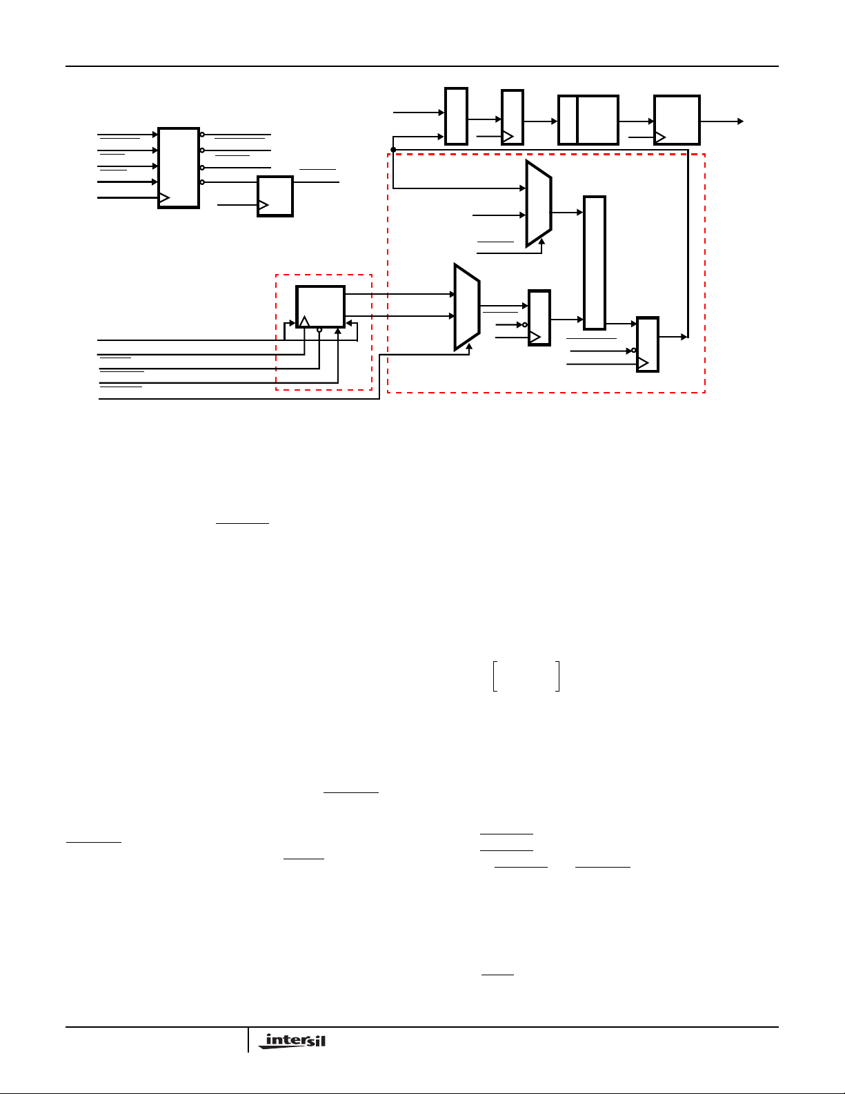
FIGURE 1. NCO-12 FUNCTIONAL BLOCK DIAGRAM
Functional Description
The NCO12 produces a 12-bit sinusoid whose frequency
and phase are digitally controlled. The frequency of the sine
wave is determined by one of two 32-bit words. Selection of
the active word is made by
output is controlled by the two-bit input P0-1, which is used
to select a phase offset of 0, 90, 180, or 270 degrees.
As shown in the Block Diagram, the NCO12 consists of a
Frequency Control Section, a Phase Accumulator, a Phase
Offset Adder and a Sine ROM. The Frequency Control
section serially loads the frequency control word into the
frequency register. The Phase Accumulator and Phase
Offset Adder compute the phase angle using the frequency
control word and the two phase modulation inputs. The Sine
ROM generates the sine of the computed phase angle. The
format of the 12-bit output is offset binary.
Frequency Control Section
The Frequency Control Section shown in Figure 1 serially
loads the frequency data into a 64-bit, bidirectional shift
register. The shift direction is selected with the
input. When this input is high, the frequency control word on
the SD input is shifted into the register MSB first. When
MSB/LSB is low the data is shifted in LSB first. The register
shifts on the rising edge of SCLK when
timing of these signals is shown in Figures 2A and 2B.
The 64 bits of the frequency register are sent to the Phase
Accumulator Section where 32 bits are selected to control
the frequency of the sinusoidal output.
Phase Accumulator Section
The phase accumulator and phase offset adder compute the
phase of the sine wavefrom the frequency control word and
SEL_L/M. The phase of the
MSB/LSB
SFTEN is low. The
A
R.P0-1
13 MSBs
/
FRCTRL
0-31
FRCTRL
32-63
(HIGH SELECTS FRCTRL0-31, LOW SELECTS FRCTRL32-63)
D
D
E
R
0 1
13
/
CLK
/
‘0’
/
R.LOAD
ACCUMULATOR
32
/
MUX
R.TXFR
CLK
R
E
/
G
32
32
INPUT
REGISTER
13
/
MUX
0 1
R
E
/
G
R
SINE
E
ROM
G
32
A
D
D
E
R
32
R.ENPHAC
CLK
PHASE ACCUMULATOR
12
/
CLK
32
/
2-DLY
R
E
G
the phase modulation bits P0-1. The architecture is shown in
Figure 1. The most significant 13 bits of the 32-bit phase
accumulator are summed with the two-bit phase offset to
generate the 13-bit phase input to the Sine Rom. A value of
0 corresponds to 0
corresponds to a value of 180
o
, a value of 1000 hexadecimal
o
.
The phase accumulator advances the phase by the amount
programmed into the frequency control register. The output
frequency is equal to:
F
N INT
LO
NF
× 232⁄(), or=
CLK
F
OUT
---------------
2
F
CLK
32
,=
where N is the 32 bits of frequency control word that is
programmed. INT[•] is the integer of the computation. For
example,if the control wordis 20000000 hexadecimaland the
clock frequency is 30MHz, then the output frequency would
be F
/8, or 3.75MHz.
CLK
The frequency control multiplexer selects the least
significant 32 bits from the 64-bit frequency control register
when
SEL_L/M is high, and the most significant 32 bits
when
SEL_L/M is low. When only one frequency word is
desired,
SEL_L/M and MSB/LSB must be either both high
or both low. This is due to the fact that when a frequency
control word is loaded into the shift register LSB first, it
enters through the most significant bit of the register. After
32 bits have been shifted in, they will reside in the 32 most
significant bits of the 64-bit register.
When
TXFR is asserted, the 32 bits selected by the frequency
controlmultiplex erare clockedinto the phase accumulatorinput
OUT0-11
R
E
G
32
/
(EQ. 1)
(EQ. 2)
3-197
Page 4

HSP45102
register.At each clock, the contentsofthis register are summed
with the current contents of the accumulator to step to the new
phase. The phase accumulator stepping may be inhibited by
holding
ENPHAC high. The phase accumulator may be loaded
with the value in the input register by asserting
LOAD, which
zeroes the feedback to the phase accumulator.
The phase adder sums the encoded phase modulation bits
P0-1 and the output of the phase accumulator to offset the
phase by 0, 90, 180 or 270 degrees. The two bits are
encoded to produce the phase mapping shown in Table 1.
This phase mapping is provided for direct connection to the
in-phase and quadrature data bits for QPSK modulation.
SCLK
SD
SFTEN
MSB/LSB
1
0
TABLE 1. PHASE MAPPING
P0-1 CODING
P1 P0 PHASE SHIFT (DEGREES)
00 0
01 90
1 0 270
1 1 180
ROM Section
The ROM section generates the 12-bit sine value from the
13-bit output of the phase adder. The output format is offset
binary and ranges from 001 to FFF hexadecimal, centered
around 800 hexadecimal.
2
61
63
62
SCLK
SD
SFTEN
MSB/LSB
CLK
LOAD
TXFR
ENPHAC
SEL_L/M
OUT0-11
FIGURE 2A. FREQUENCY LOADING ENABLED BYSFTEN
0
61
2
1
FIGURE 2B. FREQUENCY LOADING CONTROLLED BY SCLK
1346789101152
63
62
NEW
DAT A
3-198
FIGURE 3. I/O TIMING
Page 5

HSP45102
Absolute Maximum Ratings T
Supply Voltage. . . . . . . . . . . . . . . . . . . . . . . . . . . . . . . . . . . . . +8.0V
Input, Output or I/O Voltage Applied . . . . .GND -0.5V to VCC +0.5V
ESD Classification . . . . . . . . . . . . . . . . . . . . . . . . . . . . . . . . .Class 1
Operating Conditions
Operating V oltage Range (Commercial, Industrial). . +4.75V to +5.25V
Operating Temperature Range (Commercial) . . . . . . . .0oC to 70oC
Operating Temperature Range (Industrial) . . . . . . . . -40oC to 85oC
=25oC Thermal Information
A
Thermal Resistance (Typical, Note 1) θJA (oC/W)
PDIP Package. . . . . . . . . . . . . . . . . . . . . . . . . . . . . 55
SOIC Package. . . . . . . . . . . . . . . . . . . . . . . . . . . . . 70
Maximum Junction Temperature. . . . . . . . . . . . . . . . . . . . . . . 150oC
Maximum Storage Temperature Range . . . . . . . . . .-65oC to 150oC
Lead Temperature (Soldering, 10s). . . . . . . . . . . . . . . . . . . . . 300oC
(SOIC - Lead Tips Only)
Die Characteristics
Backside Potential. . . . . . . . . . . . . . . . . . . . . . . . . . . . . . . . . . . .V
CAUTION: Stresses above those listed in “Absolute Maximum Ratings” may cause permanent damage to the device. This is a stress only rating and operationofthe
device at these or any other conditions above those indicated in the operational sections of this specification is not implied.
NOTE:
1. θJA is measured with the component mounted on an evaluation PC board in free air.
CC
DC Electrical Specifications
PARAMETER SYMBOL TEST CONDITIONS MIN MAX UNITS
Logical One Input Voltage V
Logical Zero Input Voltage V
High Level Clock Input V
Low Level Clock Input V
Output HIGH Voltage V
Output LOW Voltage V
Input Leakage Current I
Standby Power Supply Current I
Operating Power Supply Current I
CCSB
CCOP
IHC
ILC
OH
OL
VCC = 5.25V 2.0 - V
IH
VCC = 4.75V - 0.8 V
IL
VCC = 5.25V 3.0 - V
VCC = 4.75V - 0.8 V
IOH = -400µA, VCC = 4.75V 2.6 - V
IOL = +2.0mA, VCC = 4.75V - 0.4 V
VIN = VCC or GND, VCC = 5.25V -10 10 µA
I
VIN = VCC or GND, VCC = 5.25V, Note 4 - 500 µA
f = 33MHz, VIN = VCC or GND
VCC = 5.25V, Notes 2 and 4
-99mA
Capacitance T
Input Capacitance C
Output Capacitance C
NOTES:
2. Power supply current is proportional to operating frequency. Typical rating for I
3. Not tested, but characterized at initial design and at major process/design changes.
4. Output load per test load circuit with switch open and CL = 40pF.
= 25oC, Note 3
A
PARAMETER SYMBOL TEST CONDITIONS MIN MAX UNITS
FREQ = 1MHz, VCC = Open. All measure-
IN
ments are referenced to device ground
O
CCOP
-10 pF
-10 pF
is 3mA/MHz.
3-199
Page 6

HSP45102
AC Electrical Specifications V
= 5.0V ±5%, TA = 0oC to 70oC, TA = -40oC to 85oC (Note 5)
CC
-33 (33MHz) -40 (40MHz)
PARAMETER SYMBOL NOTES
Clock Period t
Clock High t
Clock Low t
SCLK High/Low t
Setup Time SD to SCLK Going High t
Hold Time SD from SCLK Going High t
Setup Time SFTEN, MSB/LSB to SCLK Going High t
Hold Time SFTEN, MSB/LSB from SCLK Going High t
Setup Time SCLK High to CLK Going High t
Setup Time P0-1 to CLK Going High t
Hold Time P0-1 from CLK Going High t
Setup Time LOAD, TXFR, ENPHAC, SEL_L/M
CP
CH
CL
SW
DS
DH
MS
MH
SS
PS
PH
t
ES
30 - 25 - ns
12 - 10 - ns
12 - 10 - ns
12 - 10 - ns
12 - 12 - ns
0-0- ns
15 - 12 - ns
0-0- ns
Note 6 16 - 15 - ns
15 - 12 - ns
1-1- ns
15 - 13 - ns
UNITSMIN MAX MIN MAX
to CLK Going High
Hold Time LOAD, TXFR, ENPHAC, SEL_L/M
t
EH
1-1- ns
from CLK Going High
CLK to Output Delay t
Output Rise, Fall Time t
OH
RF
Note 7 8 - 8 - ns
2 15 2 13 ns
NOTES:
5. AC testing is performed as follows: Input levels (CLK Input) 4.0V and 0V; Input levels (all other inputs) 0V and 3.0V; Timing reference levels
(CLK) 2.0V; All others 1.5V. Output load per test load circuit with switch closed and CL= 40pF. Output transition is measured at VOH> 1.5V
and VOL < 1.5V.
6. IfTXFR is active, care must be taken to not violate setup and hold timesas data from the shift registers may not have settled before CLK occurs.
7. Controlled via design or process parameters and not directly tested. Characterized upon initial design and after major process and/or design
changes.
AC Test Load Circuit
NOTE: Test head capacitance.
3-200
DUT
SWITCH S1 OPEN FOR I
CCSB
C
L
AND I
S
1
(NOTE)
CCOP
±
I
OH
EQUIVALENT CIRCUIT
1.5V I
OL
Page 7

Waveforms
CLK
HSP45102
t
CP
t
CH
t
CL
P0-1
LOAD,TXFR,
ENPHAC, SEL_L/M
OUT0-11
SCLK
SD
MSB/LSB,
SFTEN
t
PS
t
ES
t
SW
t
DS
t
MS
t
SS
t
DH
t
MH
t
PH
t
EH
t
OH
t
SW
t
RF
FIGURE 4.
All Intersil semiconductor products are manufactured, assembled and tested under ISO9000 quality systems certification.
Intersil semiconductor products are sold by description only. Intersil Corporation reserves the right to make changes in circuit design and/or specifications at any time without notice. Accordingly, the reader is cautioned to verify that data sheets are current before placing orders. Information furnished by Intersil is believed to be accurate and
reliable. However, no responsibility is assumed by Intersil or its subsidiaries for its use; nor for any infringements of patents or other rights of third parties which may result
from its use. No license is granted by implication or otherwise under any patent or patent rights of Intersil or its subsidiaries.
For information regarding Intersil Corporation and its products, see web site http://www.intersil.com
Sales Office Headquarters
NORTH AMERICA
Intersil Corporation
P. O. Box 883, Mail Stop 53-204
Melbourne, FL 32902
TEL: (407) 724-7000
FAX: (407) 724-7240
EUROPE
Intersil SA
Mercure Center
100, Rue de la Fusee
1130 Brussels, Belgium
TEL: (32) 2.724.2111
FAX: (32) 2.724.22.05
ASIA
Intersil (Taiwan) Ltd.
7F-6, No. 101 Fu Hsing North Road
Taipei, Taiwan
Republic of China
TEL: (886) 2 2716 9310
FAX: (886) 2 2715 3029
3-201
 Loading...