

Page 1

1
16XCLK
2
TXD
3
RCV
4
A0
16
V
CC
15
OSCIN
14
OSCOUT
13
POWERDN
5
A1
6
A2
7
CLK_SEL
8
GND
12
PULSEMOD
11
IR_TXD
10
IR_RCV
9
NRST
SIR
ENCODE
SIR
DECODE
TXD IR_TXD
RCD IR_RCV
/NRST
A0
A1
A2
16XCLK
PULSEMOD
CLK_SEL
INT_CLOCK
CLOCK
DIVIDE
H
IR 3/16 Encode/Decode IC
Technical Data
HSDL-7001-2500 pc, tape
and reel
HSDL-7001#100-100pc,
50/tube
Features
• Compliant with IrDA 1.0
Physical Layer Specs
• Interfaces with IrDA 1.0
Compliant IR Transceivers
• Used in Conjunction with
Standard 16550 UART
• Transmits/Receives either
1.63 µs or 3/16 Pulse Mode
• Internal or External Clock
Modes
• Programmable Baud Rate
• 2.7-5.5 V Operation
• 16 Pin SOIC Package
Applications
• Interfaces with IR
Transceivers in:
- Computer Applications:
Notebook Computers
Sub-notebooks
Desktop PCs
PDAs
Printers
Dongle or other RS-232
adapter
- Telecom Applications:
Modems
Fax Machines
Pagers
Phones
- Handheld Data Collection:
Industrial
Medical
Transportation
Description
The HSDL-7001 modulates and
demodulates electrical pulses
from Hewlett-Packard’s
HSDL-1001 Infrared transceiver
module and other IrDA-compliant
transceivers. The HSDL-7001 can
be used with a microcontroller/
microprocessor that has a serial
communication interface (UART).
Prior to communication, the
processor selects the transmission baud rate. Serial data is then
transmitted or received at the
prescribed data rate.
The HSDL-7001 consists of two
state machines – the SIR (Serial
InfraRed) Encode and SIR Decode
blocks. It also contains a
sequential block Clock Divide
which synthesizes the required
internal signal.
The HSDL-7001 can be placed
into the Internal Clock Mode or
External Clock Mode. An external
crystal is needed for the Internal
Clock Mode. In applications
where the external 16XCLK
signal is provided, a crystal is not
needed.
There are two data transmission
modes. Data can be transmitted
and received in either a standard
3/16 modulation mode or a
1.63 µs pulse mode.
Schematic
Pin Out
Page 2

I/O Pinout List
Pin Name Type Function
1 16XCLK DIGIN Positive edge triggered input clock that is set to 16 times the data
(SIXTNCK) transmission baud rate. The encode and decode schemes require this
signal. The signal is usually tied to a UART’s BAUDOUT signal. The
16XCLK may be provided by application circuitry if BAUDOUT is not
available. This signal is required when the internal clock is not used.
2 /TXD DIGIN Negative edge triggered input signal that is normally tied to the SOUT
signal of the UART (serial data to be transmitted). Data is modulated
and output as IR_TXD.
3 RCV DIGOUT Output signal normally tied to SIN signal of a UART (received serial
data). RCV is the demodulated output of IR_RVC.
4 A0 DIGIN Clock Multiplex Signal
5 A1 DIGIN Clock Multiplex Signal
6 A2 DIGIN Clock Multiplex Signal
7 CLK_SEL DIGIN Used to activate either the Internal or External Clock. A high on this
line activates the External clock (16XCLK) and a low activates the
Internal clock. When the External clock is activated, the internal
oscillator is put in POWERDOWN MODE.
8 GND Chip Ground
9 /NRST DIGIN Active low signal used to reset the IrDA-SIR DECODE state machine.
This signal can be tied to POR (Power On Reset) or VCC. This signal can
also be used to disable any data reception.
10 /IR_RCV DIGIN Input from SIR optoelectronics. Input signal is a 3/16th or 1.6 µs pulse
which is demodulated to generate RCV output signal.
11 IR_TXD DIGOUT This is the modulated TXD signal.
12 PULSEMOD DIGIN A high level on this input puts the chip into the monoshot transmit
(with mode. In this mode, when there is a negative transition on the TXD
pulldown) input, a rising edge on the internal transmit modulation state machine
will activate a high pulse on IR_TXD for 6 crystal clock cycles. With a
3.6864 MHz crystal, this corresponds to 1.63 µs. This mode cannot be
used in conjunction with the 16XCLK clock. It is meant to be used with
the external crystal clock. By default, this input pin is pulled to GND.
13 POWERDN DIGIN A high on this input puts only the internal oscillator cell (OSCII) in
(with POWERDOWN MODE. The cell is normally not powered down.
pulldown)
14 OSCOUT ANAOUT Oscillator Output
15 OSCIN ANAIN Oscillator Input
16 V
CC
Power
Note: There are two methods of putting the internal oscillator cell in POWERDOWN MODE. Whenever the CLKSEL Pin is asserted
high (External clock selected) the oscillator cell is automatically put in powerdown mode, or whenever the POWERDN Pin is asserted
high.
Page 3

–A–
NOTES:
1. DIMENSIONS A AND B ARE DATUMS
AND T IS A DATUM SURFACE.
2. DIMENSIONING AND TOLERANCING PER
ANSI Y14.5M, 1982.
3. CONTROLLING DIMENSION: MILLIMETER.
4. DIMENSION A AND B DO NOT INCLUDE
MOLD PROTRUSION.
5. MAXIMUM MOLD PROTRUSION 0.15 (0.006)
PER SIDE.
P
–B–
G
D
0.25 (0.010)φMTBSAS
–T–
16 PL.
K
SEATING
PLANE
C
18
16 9
0.25 (0.010)φMBM
R X 45°
F
J
M
MILLIMETERS INCHES
MIN.
9.80
3.80
1.35
0.35
0.40
1.27 BSC
0.19
0.10
0°
5.80
0.25
MAX.
10.00
4.00
1.75
0.49
1.25
0.25
0.25
7°
6.20
0.50
DIM.
A
B
C
D
F
G
J
K
M
P
R
MIN.
0.386
0.150
0.054
0.014
0.016
0.060 BSC
0.008
0.004
0°
0.229
0.010
MAX.
0.393
0.157
0.068
0.019
0.049
0.009
0.009
7°
0.244
0.019
R
8 PL.
16
1
Table 1. Selection of Internal Clock Rate from Crystal Oscillator
Selected Clock Rate (bps) A2 A1 A0 Crystal Freq. Division
115200 0 0 0 Divided by 2
57600 0 0 1 Divided by 4
19200 0 1 0 Divided by 12
9600 0 1 1 Divided by 24
38400 1 0 0 Divided by 6
4800 1 0 1 Divided by 48
2400 1 1 0 Divided by 96
TEST PURPOSE 1 1 1 No division
Package Dimensions
Page 4
Encoding Scheme
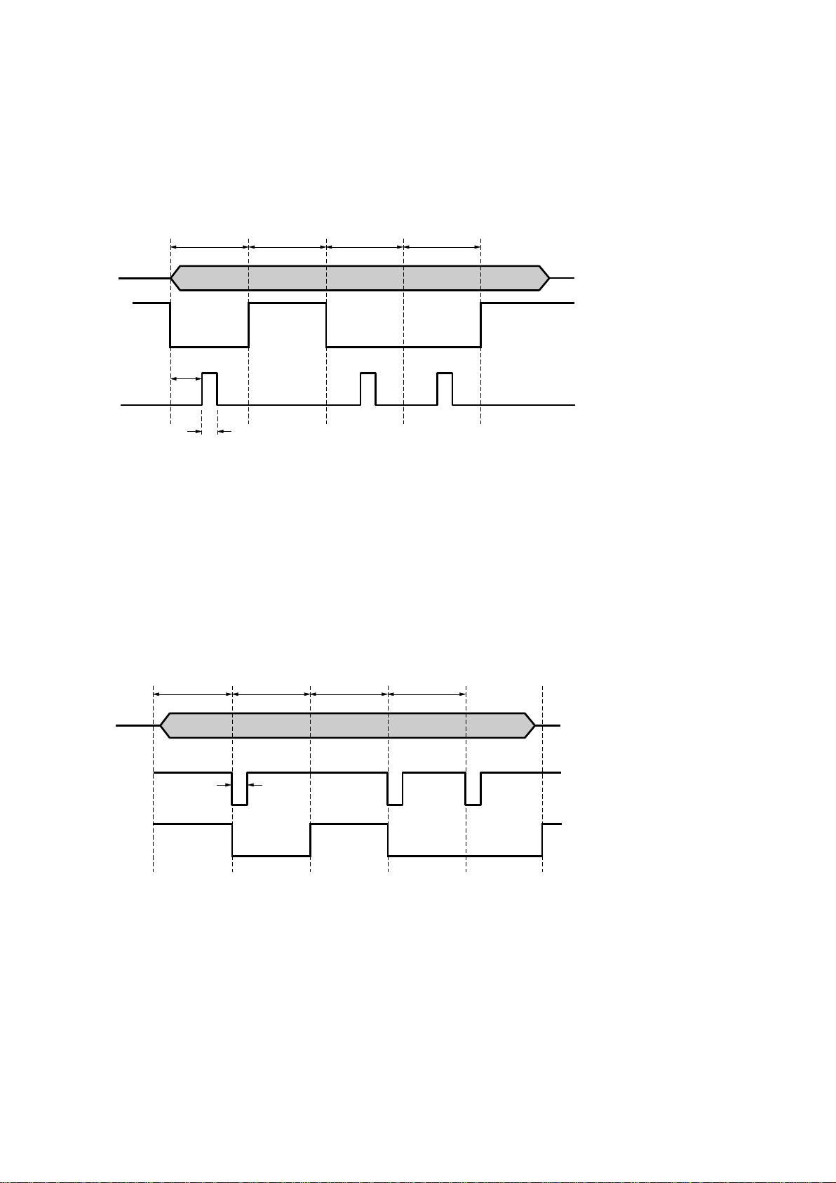
The encoding scheme relies on a
clock being present, which is set
to 16 times the data transmission
baud rate (16XCLX). The encoder
sends a pulse for every space or
“0” that is sent on the TXD line.
On a high to low transition of the
TXD line, the generation of the
pulse is delayed for 7 clock cycles
of the 16XCLK before the pulse is
set high for 3 clock cycles (or
3/16th of a bit time) and then
subsequently pulled low. This
generates a 3/16th bit time pulse
centered around the bit of
information (“0”) that is being
transmitted.
Decoding Scheme
arrival of a pulse. This pulse
needs to be stretched to
accommodate 1 bit time (or 16
16XCLK cycles). Every pulse that
is received is translated into a “0”
or space on the RXD line equal to
1 bit time.
The IrDA-SIR (Serial InfraRed)
decoding modulation method can
be thought of as a pulse stretching scheme.
Every high to low transition of
the IR_RXD line signifies the
For consecutive spaces, pulses
with a 1 bit time delay are generated in series. If a logic 1 (mark)
is sent then the encoder does not
generate a pulse.
Note 1: The stretched pulse must
be at least 3/4 of a bit time in
duration to be correctly interpreted by a UART.
Note 2: It is recommended that
TXD remains high when not
transmitting. This ensures the
LED is off and will not interfere
with signal reception.
16XCLK
16 CYCLES
TXD
IRTXD
7 CS
3 CS
16 CYCLES 16 CYCLES 16 CYCLES
16XCLK
16 CYCLES
IRRXD
RXD
3 CS
16 CYCLES 16 CYCLES 16 CYCLES
Page 5
CRYSTAL
CLK
6 CRYSTAL CYCLES
INT CLK
(DIVBY2)
TXD
INTERNAL
IRTXD
OUTPUT
IRTXD
(MONOSHOT)
1234567891011121314151617181920212223242526
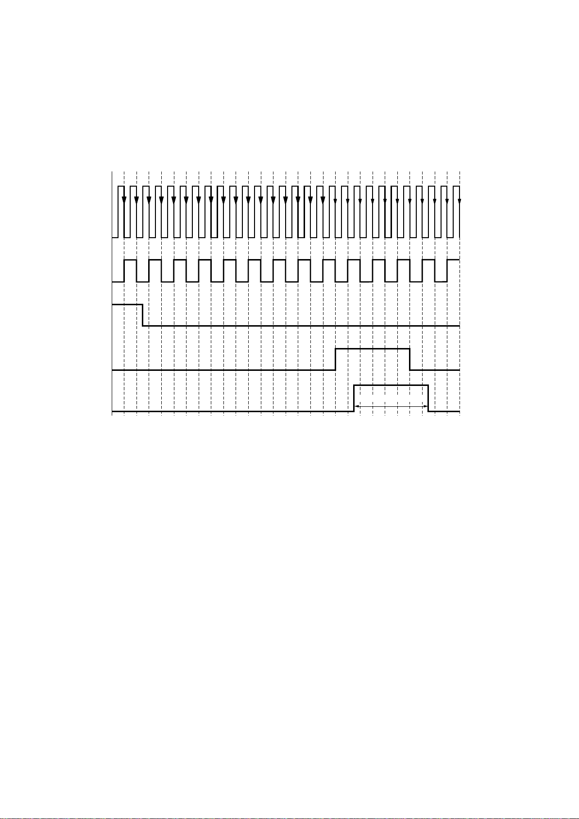
The figure above illustrates the
operation of the monoshot when
the internal clock is set to divide
by 2 mode, i.e., when A2=0,
A1=0, and A0=0. A rising edge
on the internal modulation state
machine (IRTXD OUTPUT), will
cause the output on the IRTXD to
go up for 6 crystal clock cycles.
Monoshot Operation
With a 3.6864 MHz clock, this
corresponds to a pulse of 1.63 µs.
The duration of this pulse is
independent of the code A2,
A1,A0 and is always 6 clock
cycles of the crystal, corresponding to the monoshot
operation.
Page 6
Absolute Maximum Ratings
Parameter Symbol Min. Max. Units
Storage Temperature T
S
-65 +150 °C
Operating Temperature T
A
-40 +85 °C
Output Current I
O
-100 100 mA
Power Dissipation
[1]
P
MAX
0.46 W
Input/Output Voltage
[2]
VI/V
O
-0.5 VCC + 0.5 V
Power Supply Voltage V
CC
-0.5 7.0 V
Electrostatic Protection V
ESD
4000 V
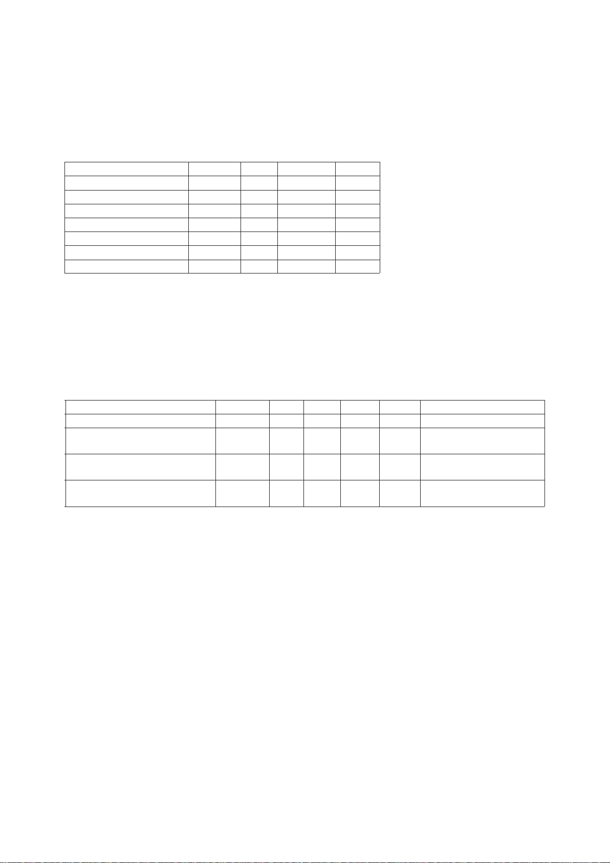
Notes:
1. Maximum power dissipation is given for Rth = 140 C/W (SO 16 Plastic).
2. All pins are protected from damage to static discharge by internal diode clamps to
VCC and GND.
Switching Specifications
(VCC = 2.7 to 5.5 V, TA = -20 to +85°C)
Parameter Symbol Min. Typ. Max. Units Conditions
Propagation Delay Time
[1]
t
pd
80 ns
Output Rise Time
[2]
t
rise
3.7 7.25 11.6 ns VCC = 5.5 V, CL = 50 pF
10 16 24 VCC = 2.7 V, CL = 50 pF
Output Fall Time
[3]
t
fall
4.4 8.35 11.2 ns VCC = 5.5 V, CL = 50 pF
11 16 26 VCC = 2.7 V, CL = 50 pF
Output Capacitance on Output C
OUT
50 pF
Pads Used for Simulation
Notes:
1. Propagation Delay Time in the output buffer is the time taken from the input passing VCC/2 to the time of the output reaching
VCC/2 with 50 pF as the output load.
2. The Output Rise Time is the time taken for the outputs (RCV, IR_TXD) to rise from 10% of the original value to 90% of the final
value.
3. The Output Fall Time is the time taken for the outputs (RCV, IR_TXD) to fall from 90% of the original value to 10% of the final
value.
Page 7
Recommended Operating Conditions
(VCC = 2.7 to 5.5 V, TA = -20 to +85°C)
Parameter Symbol Min. Typ. Max. Units Conditions
Supply Voltage V
CC
2.7 5 5.5 V
Input Voltage V
I
0.0 V
CC
V
Ambient Temperature T
A
-20 +85 °C
High Level Input Voltage V
IH
0.7 V
CC
V
CC
V
Low Level Input Voltage V
IL
0 0.3 V
CC
V
Output High Voltage V
OH
2.2 V VCC = 2.7 V
ioh = 2 mA
Output Low Voltage V
OL
0.5 V VCC = 2.7 V
iol = 2 mA
Output High Voltage V
OH
4.5 V VCC = 5.5 V
ioh = 2 mA
Output Low Voltage V
OL
0.5 V VCC = 5.5 V
iol = 2 mA
Static Power Dissipation P
STAT
0.44 0.61 mW VCC = 5.5 V
0.11 0.15 mW VCC = 2.7 V
Dynamic Power Dissipation P
DYN
11 16.5 mW VCC = 5.5 V
5.4 8.1 mW VCC = 2.7 V
Static Current Consumption I
STAT
80 110 µAVCC = 5.5 V
40 54 µAVCC = 2.7 V
Dynamic Current Consumption I
DYN
23mAV
CC
= 5.5 V
23mAV
CC
= 2.7 V
Max Clk Frequency (16XCLK)
[1]
f
16XCLK
2 MHz
Minimum Pulse Width (IR_TXD)
[2]
t
mpw
1630 ns
Pulse Width on Monoshot t
mpw
1630 1710 1730 ns
(IR_TXD and IR_RCV)
Value of Pulldown Resistor Used on R
DWN
114 152 256 KΩ
POWERDOWN & PULSEMOD Input Pins
Trigger Low Level Input Voltage VIL_TRIG 0.7 0.8 0.9 V VCC = 2.7 V
(For /NRST Input Pin) 1.9 1.95 2.00 VCC = 5.5 V
Trigger High Level Input Voltage VIH_TRIG 1.7 1.85 1.9 V VCC = 2.7 V
(For /NRST Input Pin) 3.25 3.4 3.60 VCC = 5.5 V
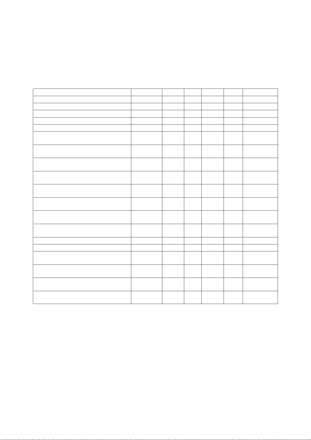
Notes:
1. IrDA Parameters. The Max Clk Frequency represents the maximum clock frequency to drive the HSDL-7001’s internal state
machine. Under normal circumstances, the clock input should not exceed 16* 115.2 Kbps or 1.8432 MHz. This product can
operate at higher clock rates, but the above is the recommended rate.
2. The Minimum Pulse Width (t
mpw
) represents the minimum pulse width of the encoded IR_TXD pulse (and the IR_RCV pulse). As
per the IrDA specifications, the minimum pulse width of the IR_TXD and IR_RCV pulses should be 3*(1/1.8432 MHz) or 1.63 µs.
Page 8
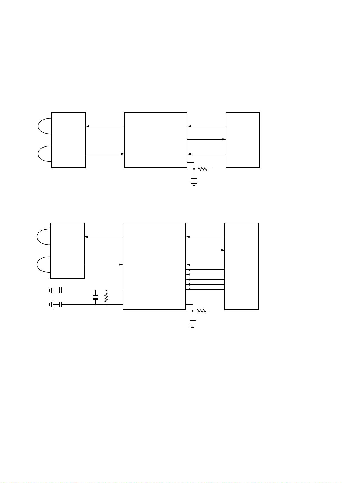
TXD
HSDL-1001 HSDL-7001
RCV
IR_TXD
IR_RCV
SDO
I01
TXD
A0
RCV
MICROCONTROLLER
SDI
V
CC
10 kΩ
0.1 µF
I02A1
I03A2
I04CLK_SEL
I05PULSEMOD
I06POWERDN
F = 3.6864 MHz
10 MΩ
15 pF
15 pF
OSCIN
OSCOUT
NRST
NOTE: POWERDN CAN BE USED AS A BASIC CHIP SELECT.
THE HSDL-7001 WILL NOT BE ABLE TO RECEIVE OR TRANSMIT DATA WHILE POWERDN IS ASSERTED.
H
Application Circuits
HSDL-7001 Connection to UART
For technical assistance or the location of
your nearest Hewlett-Packard sales office,
distributor or representative call:
Americas/Canada: 1-800-235-0312 or
408-654-8675
Far East/Australasia: Call your local HP
sales office.
Japan: (81 3) 3335-8152
Europe: Call your local HP sales office.
Data subject to change.
Copyright © 1996 Hewlett-Packard Co.
Printed in U.S.A. 5965-5150E (11/96)
HSDL-7001 Connected to Microcontroller
TXD
HSDL-1001 HSDL-7001
RCV
IR_TXD
IR_RCV
SOUT
BAUDOUT
TXD
16XCLK
RCV
UART 16550
SIN
V
CC
10 kΩ
0.1 µF
NRST
 Loading...