

Page 1
Infrared IrDA
Compliant Transceiver
Technical Data
HSDL-1001
Features
• Fully Compliant to
IrDA 1.0 – 115 Kb/s
• Compatible with ASK,
Consumer IR/TV Remote
• Superb Nose-to-Nose
Operation
• Low Power Consumption
3 µA in Shutdown
• Supply Voltage Range
2.7 V – 5.5 V
• Operational Down to 2 V
• Free Netlist for IrDA
Modulation Circuitry
• Low Latency 100 µs
• Available in Tape & Reel
for Auto Insertion
• Drop in Replacement for
HSDL-1000
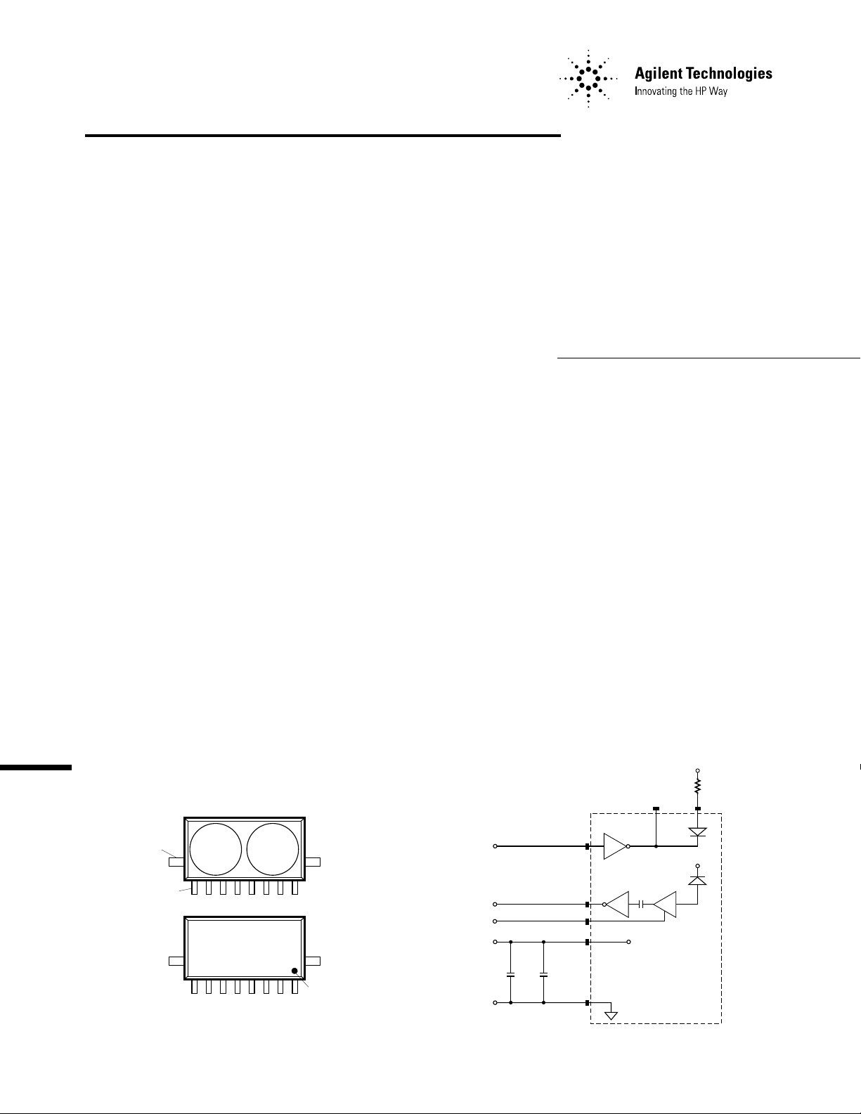
BUTTRESS
LEAD*
PIN 1
1001
YYWW
Description
The HSDL-1001 infrared
transceiver provides the interface
between logic and IR signals for
through-air, serial, half-duplex IR
data links and is designed to
satisfy the IrDA Physical Layer
Specification for data rates up to
115 Kb/s.
The HSDL-1001 contains a high
speed, high efficiency TS AlGaAs
875 nm LED, a silicon PIN
photodiode and a bipolar, silicon
TXD
RXD
SHUTDOWN
V+
PIN 1
INDICATOR
GND
integrated circuit. The IC contains
an LED driver, amplifiers and
a quantizer.
The shutdown function permits
operating the receiver in a
low current mode to minimize
battery drain.
Applications for the HSDL-1001
include notebook PCs, telephones,
pagers, printers, cameras, and
industrial handheld devices.
LEDC
TXD
COMPARATOR
RXD
SD
V
CC
CX3CX4
GND
LED
PHOTODIODE
V
V+
PIN
R
LED
LEDA
* SIDE BUTTRESS LEADS ARE FOR MECHANICAL STABILITY AND
SHOULD NOT BE CONNECTED TO ANY ELECTRICAL POTENTIAL.
Page 2
2
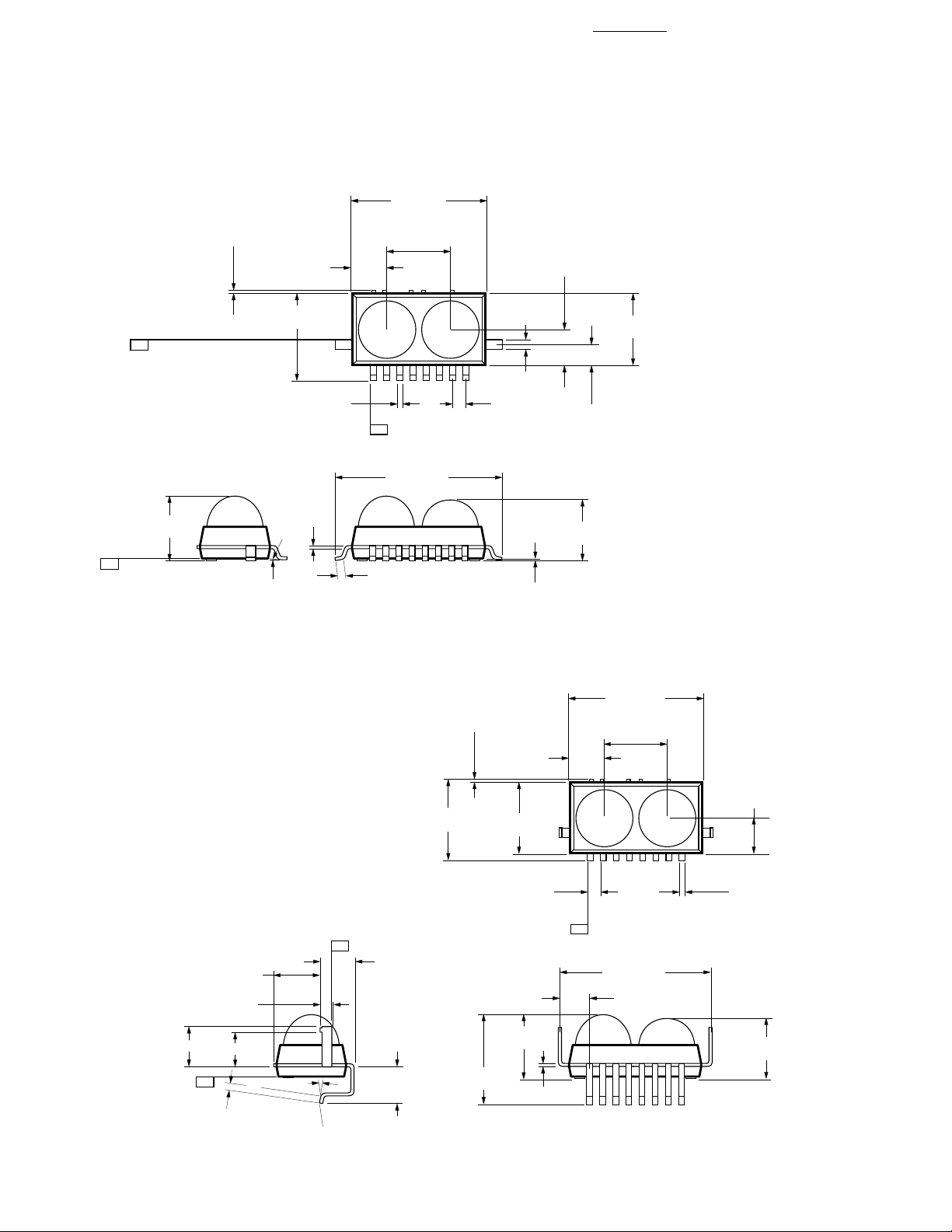
Package Dimensions
Option 0X1*
0.43
MAX.
(0.017)
8.54 ± 0.15
(0.336 ± 0.01)
-B-
0.51 ± 0.08
(0.020 ± 0.003)
6.22 ± 0.25
(0.24 ± 0.01)
-A-
5.0° ± 3° (10x)
DIMENSIONS IN MILLIMETERS (INCHES).
3.4 ± 0.25
(0.14 ± 0.01)
MAX.
0.25
1 2345678
(8x)
-C-
0.6 ± 0.12
(0.02 ± 0.005)
13.21 ± 0.25
(0.52 ± 0.01)
6.4 ± 0.25
(0.25 ± 0.01)
16.61 ± 0.15
(0.654 ± 0.01)
(10x)
3.4 ± 0.25
(0.14 ± 0.01)
0.9 ± 0.25
(0.04 ± 0.01)
1.27 ± 0.10
(0.050 ± 0.004)
0.13 ± 0.05
(0.005 ± 0.002)
(7x)
1.9 ± 0.25
(0.08 ± 0.01)
5.94 ± 0.25
(0.23 ± 0.01)
6.86 ± 0.25
(0.27 ± 0.01)
Option 0X2*
NOTE:
THE -B- DATUM IS FORMED BY THE
TWO HIGHEST POINTS OF THE COMBINDED
SURFACE FORMED BY THIS SURFACE AND
THE CORRESPONDING SURFACE OF THE
SAME LEAD ON THE OPPOSITE SIDE
OF THE PACKAGE.
0 = TAPE AND REEL.
X = STRIP OF 10.
1 = JEDEC STANDARD ARRAY.
4.00 ± 0.15
4.56 ± 0.15
(0.180 ± 0.01)
1.12 ± 0.15
(0.44 ± 0.006)
3.4 ± 0.15
-A-
0.60 ± 0.12
(0.02 ± 0.005)
5.0° ± 3° (8x)
0.43
MAX.
(0.017)
3.4 ± 0.25
(0.14 ± 0.01)
7.92 ± 0.25
(0.312 ± 0.01)
-B-
3.24 ± 0.25
(0.128 ± 0.01)
3.80 ± 0.15
(0.150 ± 0.01)
COPLANARITY ± 0.05 mm (0.002 INCHES).
MAX.
6.86 ± 0.25
(0.27 ± 0.01)
1.27 ± 0.10
(0.05 ± 0.004)
6.22 ± 0.25
(0.24 ± 0.01)
8.88 ± 0.15
(0.349 ± 0.01)
DIMENSIONS IN MILLIMETERS (INCHES).
(7x)
0.25
13.21 ± 0.25
(0.52 ± 0.01)
6.4 ± 0.25
(0.25 ± 0.01)
1 2345678
-C-
15.13 ± 0.25
(0.596 ± 0.01)
3.12 ± 0.15
(0.123 ± 0.01)
3.43 ± 0.25
(0.14 ± 0.01)
0.51 ± 0.08
(0.020 ± 0.003)
5.94 ± 0.25
(0.23 ± 0.01)
(8x)
Page 3
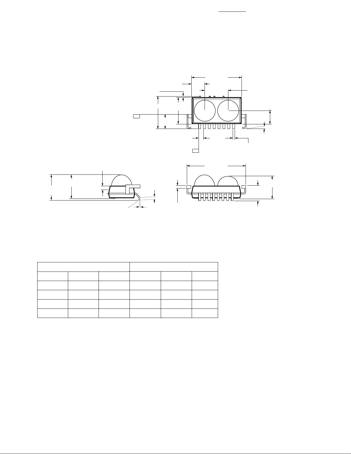
Package Dimensions (continued)
Option X04
0.43 (0.02) MAX.
NOTE:
THE -B- DATUM IS FORMED BY THE
TWO HIGHEST POINTS OF THE COMBINED
SURFACE FORMED BY THIS SURFACE AND
THE CORRESPONDING SURFACE OF THE
SAME LEAD ON THE OPPOSITE SIDE
OF THE PACKAGE.
*X POSITION INDICATES PACKAGING.
0 = TAPE AND REEL.
1 = JEDEC STANDARD ARRAY.
8.75 ± 0.15
(0.345 ± 0.01)
-B-
3.43 ± 0.25
(0.14 ± 0.010)
MAX.
3.84
(0.151)
1.27 ± 0.15
(0.050 ± 0.01)
6.86 ± 0.25
(0.27 ± 0.01)
13.21 ± 0.25
(0.52 ± 0.01)
1 2345678
(7x)
-C-
3
0.51 ± 0.08
(0.020 ± 0.003)
6.35 ± 0.25
(0.25 ± 0.010)
3.43 ± 0.25
(0.14 ± 0.010)
5.0° ± 3.5°
(8x)
(2x)
15.89 ± 0.15
(0.626 ± 0.01)
6.79 ± 0.25
(0.27 ± 0.01)
6.22 ± 0.25
(0.24 ± 0.01)
APPROX.
COPLANARITY
± 0.076 mm (0.003 INCHES).
0.90 ± 0.25
(0.04 ± 0.01)
CG
0.61 ± 0.25
(0.02 ± 0.01)
0.76 ± 0.08
5.00°
DIMENSIONS IN MILLIMETERS (INCHES).
(0.030 ± 0.003)
Truth Table
Inputs Outputs
TXD EI
V
IH
V
IL
V
IL
V
IL
X = Don’t care
NV = Not Valid
Notes:
1. EI – Irradiance (light intensity) present at detector surface.
2. For in-band IrDA signals ≤ 115 kb/s.
3. RXD Low is a pulsed response. The condition is maintained for a duration dependent
on the pattern and strength of the incident signal.
[1]
SD IE(LED) LEDA RXD
X X High (On) Low NV
[2]
EI
EI
IH
IL
V
IL
V
IL
Low (Off) High Low
Low (Off) High High
XVIHLow (Off) High High
[3]
5.93 ± 0.25
(0.23 ± 0.01)
4.12 ± 0.15
(0.162 ± 0.006)
Page 4
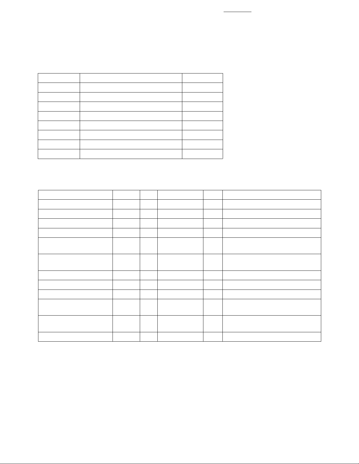
Pinout
Pin Description Symbol
1 Shutdown SD
2 No Connection
3 Supply Voltage V
4 Receiver Data Output RXD
5 Ground Gnd
6 Transmitter Data Input TXD
7 LED Cathode LEDC
8 LED Anode LEDA
Absolute Maximum Ratings
4
CC
Parameter Symbol Min. Max. Units Conditions
Storage Temperature T
Operating Temperature T
S
A
-20 85 °C
070°C
Lead Solder Temperature 260 °C For 10 s (1.6mm below seating plane)
Average LED Current I
Repetitive Pulsed LED I
(DC) 100 mA
LED
(RP) 500 mA ≤ 90 µs Pulse Width,
LED
Current ≤ 20% Duty Cycle
Peak LED Current I
(PK) 1.0 A ≤ 2 µs Pulse Width,
LED
≤ 10% Duty Cycle
LED Anode Voltage V
LED Cathode Voltage V
Supply Voltage V
Transmitter Data Input V
LEDA
LEDC
CC
TXD
-0.5 7.0 V
-0.5 V
LEDA
0 7.0 V
-0.5 VCC, 5.5 V
V
Voltage
Receiver Data Output V
RXD
-0.5 (VCC + 0.5), 5.5 V
Voltage
Shutdown V
SD
-0.5 VCC, 5.5 V
Page 5
5
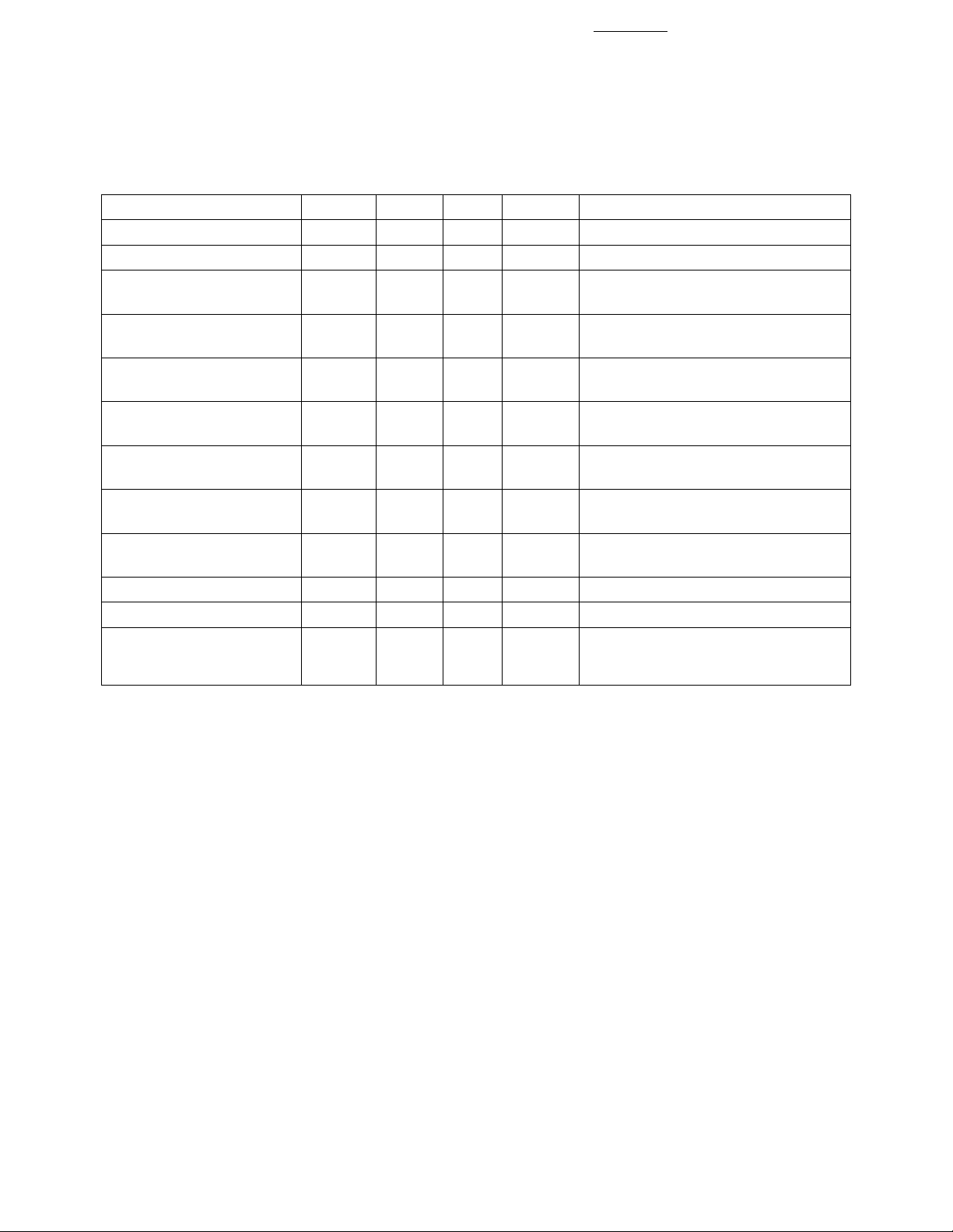
Recommended Operating Conditions
Parameter Symbol Min. Max. Units Conditions
Operating Temperature T
Supply Voltage V
A
CC
Logic High Transmitter VIH(TXD) 2.5 V
Input Voltage
Logic Low Transmitter VIL (TXD) 0.0 0.8 V
Input Voltage
Logic Low Shutdown VIL(SD) 0.0 0.8 V
Input Voltage
Logic High Shutdown VIH(SD) 2.5 V
Input Voltage
Logic High Receiver EI
IH
Input Irradiance
Logic Low Receiver EI
IL
Input Irradiance
LED (Logic High) Current I
LEDA
Pulse Amplitude
Receiver Set-up Time 200 µs For full sensitivity after transmitting
Signal Rate RXD 2.4 115 Kp/s
Ambient Light See IrDA Serial Infrared Physical
070°C
2.7 5.5 V
CC
CC
V
V
0.0036 500 mW/cm2For in-band signals*
0.3 µW/cm2For in-band signals*
240 mA For one metre links with daylight filters
Layer Link Specification, Appendix A
for ambient levels.
*Note: An in-band optical signal is a pulse/sequence where the peak wavelength, λp, is defined as 850 nm ≤ λp ≤ 900 nm, the pulse
repetition rate, PRR, is defined as 2.4 Kp/s ≤ PRR ≤ 115.2 Kp/s and the pulse width, PW, is defined as 1.6 µs ≤ PW ≤ (3/16)/PRR.
Page 6
6
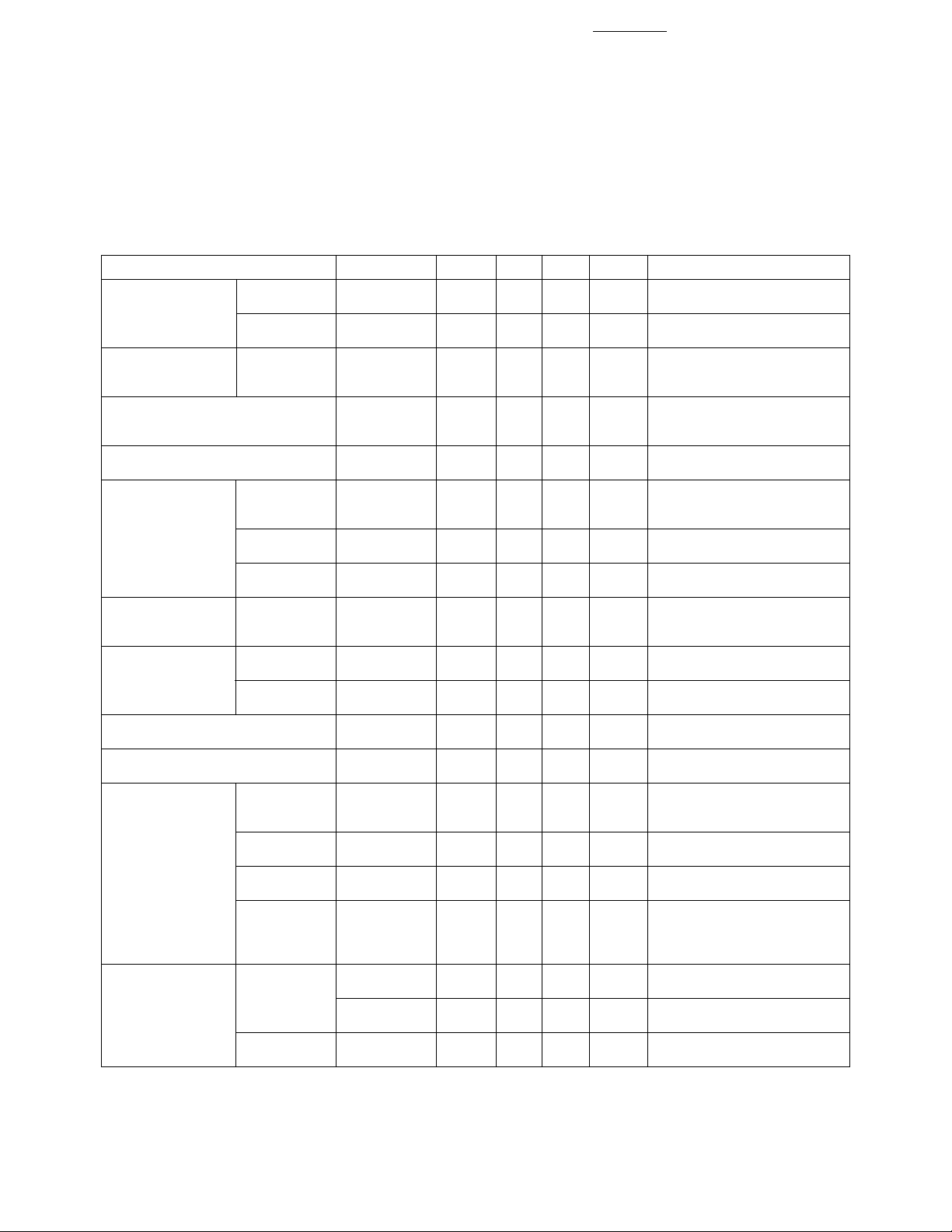
Electrical & Optical Specifications
Specifications hold over 3.0 V ≤ VCC ≤ 5.5 V and 0°C ≤ TA ≤ 70°C and all typicals are at VCC = 5.0 V and
TA = 25°C unless otherwise specified. Listed conditions represent worst case values for the parameters
under test. Unspecified test conditions can be anywhere in their recommended operating range.
Parameter Symbol Min. Typ. Max. Unit Conditions
Receiver Data Logic Low
[2]
VOL(RXD)
Output Voltage W/cm2, ϕ1/2 ≤ 15°
Logic High VOH(RXD) VCC-0.6 V Iο = -20 µA, for in-band EI
Receiver Field Twice Half- 2ϕ1/
of View Angle angle where receiver
Receiver Peak λp(EI) 880 nm
Sensitivity
Wavelength
Effective Detector 0.16 cm
Area
Transmitter Logic High IEH I
Radiant Intensity Intensity 55 mW/SR TA = 25°C
Peak λp(IE) 875 nm
Wavelength
Spectral Line ∆λ1/
Half Width
Transmitter Field Twice Half- 2θ1/
of Emission Angle where radiant intensity =
Transmitter Data Logic Low IIL(TXD) -1.0 5.0 µA0 ≤ VI ≤ 0.8 V
Input Current
Logic High IIH(TXD) 40 100 µAVI = 2.5 V
LED Anode On VON(LEDA) 2.1 2.50 V I
State Voltage Tj = 25°C
LED Anode Off ILK(LEDA) <0.2 10 µAV
State Leakage VI = 0.3 V
Supply Current Idle I
Active I
Receiver EI = EIIH, VI(TXD) = V
Active I
Transmitter EI = EIIL, VI(TXD) = V
Shutdown ICC(SD) 3 14 µAVCC = 3.6 V
Shutdown Logic High IIH(SD) 2.5 10 µAVCC = 5.5 volts
Input Current VSD = 5.5 volts
Logic Low IIL(SD) -1.0 1 µA 3.0 V ≤ VCC ≤ 5.5 V
2
[1,2]
30 ° Half-angle, ϕ1/2, is the
0.4 V For in-band EI ≥ 3.6 µ
≤ 0.3 µW/cm
2
sensitivity = 3.6 µW/cm2.
2
= 240 mA, VI = 2.5 V
LEDA
44 109 250 mW/SR 0°C ≤ TA ≤ 70°C
2
2
30 60 ° Half-angle, θ1/2, is the angle
35 nm
44 mW/SR.
125 250 µAVI = 5.0 V
= 240 mA,
LEDA
= VCC = 5.5 V,
LEDA
CC1
190 260 µAVCC = 3.6 V
210 290 µAVCC = 5.5 V,
EI = EIIL, VI (TXD) = V
CC2
CC3
0.22 25 mA VCC = 5.5 V,
10 mA VCC = 5.5 V,
520µAVCC = 5.5 V,
EI = EIIL, VI(TXD) = VIL,
VSD = V
IH
IIH(SD) 2 8 µAVCC = 3.6 volts
VSD = 3.6 volts
0 V ≤ VSD ≤ 0.8 V
IL
IL
IH
Notes:
1. Pulsed Response — Logic Low is a pulsed response. A receiver output low state VOL(RXD) is not indefinitely maintained but is instead
a pulsed response. The output low state is maintained for a duration dependent on the incident bit pattern and incident intensity (EI).
2. The EI ≥ 3.6 µW/cm2 condition guarantees the IrDA minimum receiver sensitivity of 4.0 µW/cm2 while allowing for 10% light loss
through a cosmetic window placed in front of the HSDL-1001.
Page 7
7
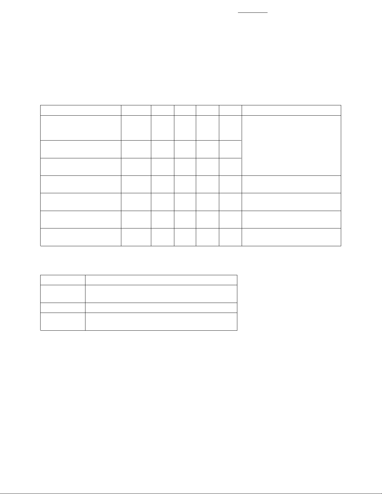
Switching Specifications
Specifications hold over 3.0 V ≤ VCC ≤ 5.5 V and 0 ≤ TA ≤ 70°C and all typicals are at VCC = 5.0 V and T
= 25°C unless otherwise specified. Listed conditions represent worst case values for the parameters under
test. Unspecified test conditions can be anywhere in their recommended operating range.
Parameter Symbol Min. Typ. Max. Units Conditions
Transmitter Optical tpw(SD) 1.45 1.7 2.15 µsR
Pulse Width 2.5 V ≤ VIH(TXD) ≤ V
Transmitter Optical tr(SD) 0.05 0.6 µs
Rise Time
Transmitter Optical tf(SD) 0.1 0.6 µs
Fall Time
Receiver Pulse tpw(RXD) 0.5 8.2 µs For in-band EI ≤ 115.2 Kb/s
Width
Receiver Latency tL(RXD) 100 200 µs
Time
Receiver Wake-Up twu(RXD) 40 100 µs
Time
Receiver Shutdown tsd(RXD) 10 100 µs
Time
= Recommended Value
LED
tpw(TXD) = 1.6 µs
CC
A
Application Circuit
Component Recommended Value
R
LED
CX3 0.10 µF ± 22%. XR7 Ceramic, Lead Length ≤ 5 mm.
CX4 4.7 µF minimum. Larger values recommended for
9.1 Ω, ± 5%, 0.5 W, for 4.5 V ≤ VCC ≤ 5.5 V
3.3 Ω, ± 5%, 0.5 W, for 3.0 V ≤ VCC ≤ 3.6 V
noisy supplies or environments.
Page 8

Appendix A. Test
Methods
A.1. Background Light and
Electromagnetic Field
There are four ambient
interference conditions in which
the receiver is to operate correctly.
The conditions are to be applied
separately:
1. Electromagnetic field: 3 V/m
maximum (refer to IEC 801-3.
severity level 3 for details)
2. Sunlight: 10 kilolux maximum
at the optical port
This is simulated with an IR
source having a peak wavelength
within the range 850 nm to
900 nm and a spectral width less
than 50 nm biased to provide
490 µW/cm2 (with no modulation) at the optical port. The light
source faces the optical port.
This simulates sunlight within the
IrDA spectral range. The effect
of longer wavelength radiation is
covered by the incandescent
condition.
3. Incandescent Lighting:
1000 lux maximum
This is produced with general
service, tungsten-filament, gasfilled, inside-frosted lamps in the
60 Watt to 150 Watt range to
generate 1000 lux over the
horizontal surface on which the
equipment under test rests. The
light sources are above the test
area. The source is expected to
have a filament temperature in
the 2700 to 3050 degrees Kelvin
range and a spectral peak in the
850 nm to 1050 nm range.
4. Fluorescent Lighting: 1000 lux
maximum
This is simulated with an IR
source having a peak wavelength
within the range 850 nm to
900 nm and a spectral width of
less than 50 nm biased and
modulated to provide an optical
square wave signal (0 µW/cm
2
minimum and 0.3 µW/cm2 peak
amplitude with 10% to 90% rise
and fall times less than or equal
to 100 ns) over the horizontal
surface on which the equipment
under test rests. The light sources
are above the test area. The
frequency of the optical signal is
swept over the frequency range
from 20 kHz to 200 kHz.
Due to the variety of fluorescent
lamps and the range of IR
emissions, this condition is not
expected to cover all circumstances. It will provide a common
floor for IrDA operation.
www.semiconductor.agilent.com
Data subject to change.
Copyright © 1999 Agilent Technologies Inc.
5965-5363E (11/99)
 Loading...