

Page 1
1.5 – 2.5 GHz Upconverter/
Downconverter
Technical Data
HPMX-5001
Features
• 2.7 V Single Supply Voltage
• Low Power Consumption
(60␣ mA in Transmit Mode,
39 mA in Receive Mode
Typical)
• 2 dBm Typical Transmit
Power at 1900 MHz
• Half-Frequency VCO with
Frequency Doubler
• 32/33 Dual-Modulus
Prescaler
• Flexible Chip Biasing,
Including Standby Mode
• TQFP-32 Surface Mount
Package
• Operation to 2.5 GHz
• Use with Companion
HPMX-5002 IF chip
Applications
• DECT, UPCS and ISM Band
Handsets and Basestations
Functional Block Diagram
RX IF OUT
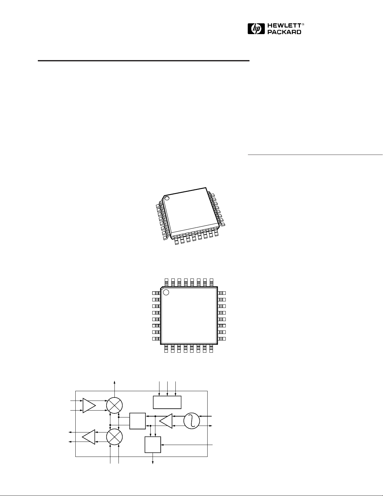
Plastic TQFP-32 Package
General Description
The HPMX-5001 Upconverter/
Downconverter provides RF
H
HPMX-5001
YYWW
XXXX ZZZ
system designers with all of the
necessary features to perform an
RF-to-IF downconversion for a
receive path, as well as an IF-toRF upconversion for transmit
mode.
Designed to meet the unique
needs of portable applications,
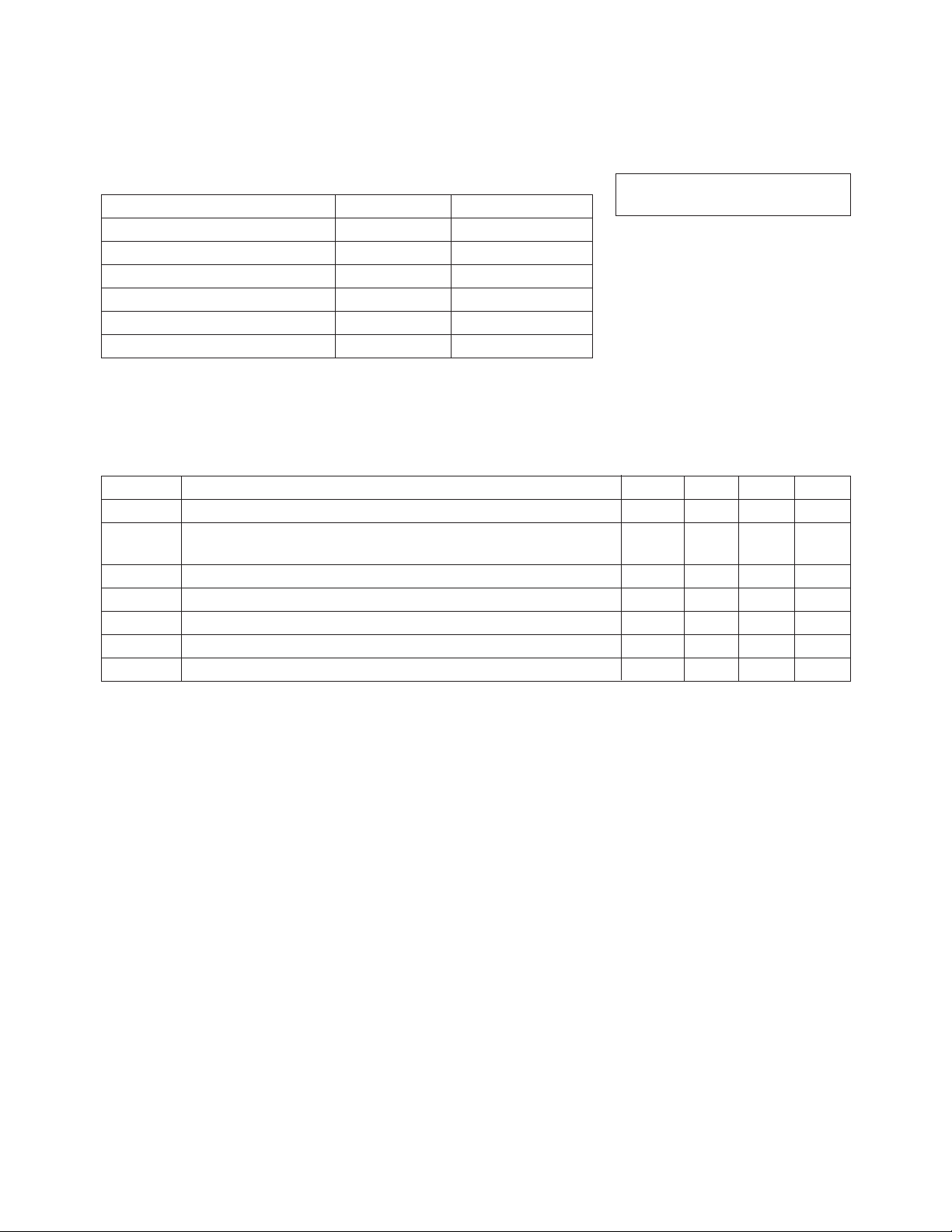
Pin Configuration
the HPMX-5001 combines the
qualities of flexible chip biasing,
32
1
H
HPMX-5001
YYWW
XXXX ZZZ
817
916
25
24
low power consumption, and true
2.7 V minimum supply voltage
operation to provide superior
performance and battery life. By
incorporating the active elements
of the VCO on-chip, as well as a
32/33 dual-modulus prescaler,
overall system component count
and costs are decreased. The
32-TQFP package insures that
this high level of integration
occupies a small amount of
POWER DOWN
CONTROL
printed circuit board space.
RX RF IN
TX RF OUT
5965-9105E
X2
32/33
TX IF IN PRESCALER
OUT
7-90
EXT.
VCO
TANK
RATIO
SELECT
The HPMX-5001 can be used in
either dual-conversion systems
(with the HPMX-5002 IF
Demodulator/Modulator) or
single-conversion systems. The
HPMX-5001 is manufactured
using Hewlett-Packard’s HP-25
Silicon Bipolar Process with
25␣ GHz fT and 30 GHz f
Max
.
Page 2
HPMX-5001 Absolute Maximum Ratings
[1]
Parameter Min. Max.
VCC Supply Voltage -0.2 V 8 V
Voltage at Any Pin
Power Dissipation
[4]
[2,3]
-0.2 V VCC + 0.2 V
RF Input Power 15 dBm
Junction Temperature +150°C
Storage Temperature -55°C +125°C
600 mW
Thermal Resistance
θjc = 100°C/W
Notes:
1. Operation of this device in excess of
any of these parameters may cause
permanent damage.
2. T
= 25°C.
CASE
3. Derate at 10 mW/°C for T
4. Except CMOS logic inputs–see
Summary Characterization Information
table.
[2]
CASE
:
>90°C.
HPMX-5001 Guaranteed Electrical Specifications
Unless otherwise noted, all parameters are guaranteed under the following conditions: VCC = 3.0 V. Test
results are based upon use of networks shown in test board schematic diagram (see Figure 28). Typical
values are for VCC = 3.0 V, TA = 25°C.
Symbol Parameters and Test Conditions Units Min. Typ. Max.
G
P
out
I
CC
V
DIV
Notes:
1. 50 Ω RF source, 100 MHz < IF < 300 MHz, 1.89 GHz RF. There is a 750 Ω resistor on chip between RXIF and RXIFB (pins 3 and 4). A
matching network from 750 Ω to 50 Ω is used for this measurement. Insertion loss of the matching network is included in the net
conversion gain figure. See Figure 28.
2. Signal injected into P3 in Figure 28 is -12.5 dBm.
3. DIV output AC coupled into a 2 kΩ || 10 pF load. See test board schematic diagram, Figure 28.
Receive Conversion Gain
C
Transmitter Power Output Input
Device Supply Current Transmit Mode mA 64 80
DIV Single-Ended Swing
[1]
[2]
d B 12 14
2:1 output VSWR dBm 0 2
Receive Mode mA 43 54
Synth Mode mA 15 19
Standby Mode (with DIVMC Set High) µA150
[3]
V
PP
0.7 1
7-91
Page 3

HPMX-5001 Summary Characterization Information
Typical values measured on test board shown in Figure 28 at VCC = 3.0 V, TA = 25°C, RXIF = 110.592 MHz,
TXRF = 1.89 GHz, unless otherwise noted.
Symbol Parameters and Test Conditions Units Typical
V
IH
V
IL
I
IH
IILCMOS Input Low Current µA > -300
t
s
t
h
t
pd
Receive Mode 1.89 GHz 2.45 GHz
Gc Receive Conversion Gain
NF Noise Figure
I
IP3
I
P1dB
VSWR
in
Transmit Mode
PIM
3
O
P1dB
VSWR
out
F
IF IF 3 dB Bandwidth MHz 500 500
3dB
Synth Mode
CMOS Input High Voltage (Can Be Pulled V ≥ V
up as High as VCC + 7 V)
[1]
CMOS Input Low Voltage V ≤ V
CC
CC
- 0.8
- 1.9
CMOS Input High Current µA< 10
[4]
[2,8]
[2,8]
[3]
[2,8]
[9]
ns 4
ns 0
ns < 7
µs< 1
dB 14 13.5
dB 10 10
DIVMC Setup Time
DIVMC Hold Time
DIV Propagation Delay
Mode Switching Time
Input Third Order Intercept Point dBm -8 -9
Input 1 dB Gain Compression Point dBm -18 -18
LO Leakage (2 x f
Input VSWR
[6]
[5]
Power Output Level for >35 dB IM3 Suppression
) at IF Port dBm -57 —
VCO
1.3:1 1.3:1
[10]
dBm — -5
Output 1 dB Gain Compression Point dBm 0 0
Output VSWR 1.8:1 1.8:1
LO Suppression (2 x f
Transmitter C/N @ 2 x f
1LO Frequency Range
) d B c 25 30
VCO
VCO
[7]
+ 4 MHz
[11]
dBc/Hz +137 +134
MH z 750-1200
Notes:
1. All CMOS logic inputs are internally pulled up to logic high level.
2. See Figure 2 for detailed timing diagram.
3. Between any two different biasing modes. This switching time does not include PLL lock-up time.
4. Single sideband noise figure.
5. In modes other than receive, the VSWR may be as high as 10:1.
6. Single-ended 50 Ω RF load, 300 Ω series IF terminations (600 Ω differential), 100 MHz < IF < 300 MHz, 1.89 GHz RF.
7. The LO is followed by a frequency doubler which raises the LO range to 1500-2400 MHz.
8. DIV output AC coupled into a 2 kΩ || 10 pF load. See test diagram, Figure 28.
9. 50 Ω RF source, 110 MHz < IF < 300 MHz, 1.89 GHz or 2.45 GHz RF. There is a 750 Ω resistor on chip between RXIF and RXIFB
(pins 3 and 4). A matching network from 750 Ω to 50␣ Ω is used for this measurement. Insertion loss of the matching network is
included in the net conversion gain figure.
10. PIM3 is the maximum SSB output power for at least 35 dB IM3 spur suppression.
11. Measured at saturated output power for 1.89 GHz. Measured at -5 dBm SSB output power for 2.45␣ GHz.
7-92
Page 4
Table 1 - HPMX-5001 Pin Description
No. Mnemonic I/O Type Description
1 TXCTRL CMOS I/P Controls biasing of transmit mixer, amplifiers, and doubler
3 RXIFB Analog O/P Inverted single-ended downconverted receiver output,
normally tied to VCC (internal 750 Ω resistor connects to RXIF)
4 RXIF Analog O/P Single-ended downconverted receiver output, drives SAW
filter (internal 750 Ω resistor connects to RXIFB)
5 TXIF Analog I/P Transmit non-inverting IF input
6 TXIFB Analog I/P Transmit inverting IF input
7 LNAREF Analog DC I/P Reference input for receive input amplifier
8 RXRF Analog I/P Receive RF input
10 TXRXVCC DC Supply Supply voltage for transmit path, receive front-end and mixer
11, 15 TXRXGND Ground Ground for transmit path, receive front-end and mixer
12 TXRFB Analog O/P Inverting output of transmit path (see test diagram for
matching network)
14 TXRF Analog O/P Non-inverting output of transmit path (see test diagram for
matching network)
16 DBLVCC DC Supply Supply voltage for LO frequency doubler
17 DBLGND Ground Ground for LO frequency doubler
20 VCOTNKS Analog I/P Sense line from external tank circuit to on-chip VCO amplifier
21 VCOTNKF Analog O/P Force line from on-chip VCO amplifier to external tank circuit
22 VCOVCC DC Supply Supply voltage for on-chip VCO amplifier
23 VCOGND Ground Ground for on-chip VCO amplifier
26 DIVVCC DC Supply Supply voltage for 32/33 dual-modulus prescaler
27 DIVGND Ground Ground for 32/33 dual-modulus prescaler
28 DIV Analog O/P Output from 32/33 dual-modulus prescaler
30 DIVMC CMOS I/P Modulus control signal for 32/33 dual-modulus prescaler
31 LOCTRL CMOS I/P Controls biasing for VCO and 32/33 dual modulus prescaler
32 RXCTRL CMOS I/P Controls biasing for receive mixer, amplifiers, and doubler
2, 9, 13, VSUB Ground Substrate bias voltage
18, 19, 24,
25, 29
Table 2 - HPMX-5001 Mode Control
(CMOS Logic Levels - all pins internally pulled up to high level)
Mode TXCTRL RXCTRL LOCTRL
Transmit 0 1 0
Receive 1 0 0
Synth 1 1 0
Standby 1 1 1
7-93
Page 5
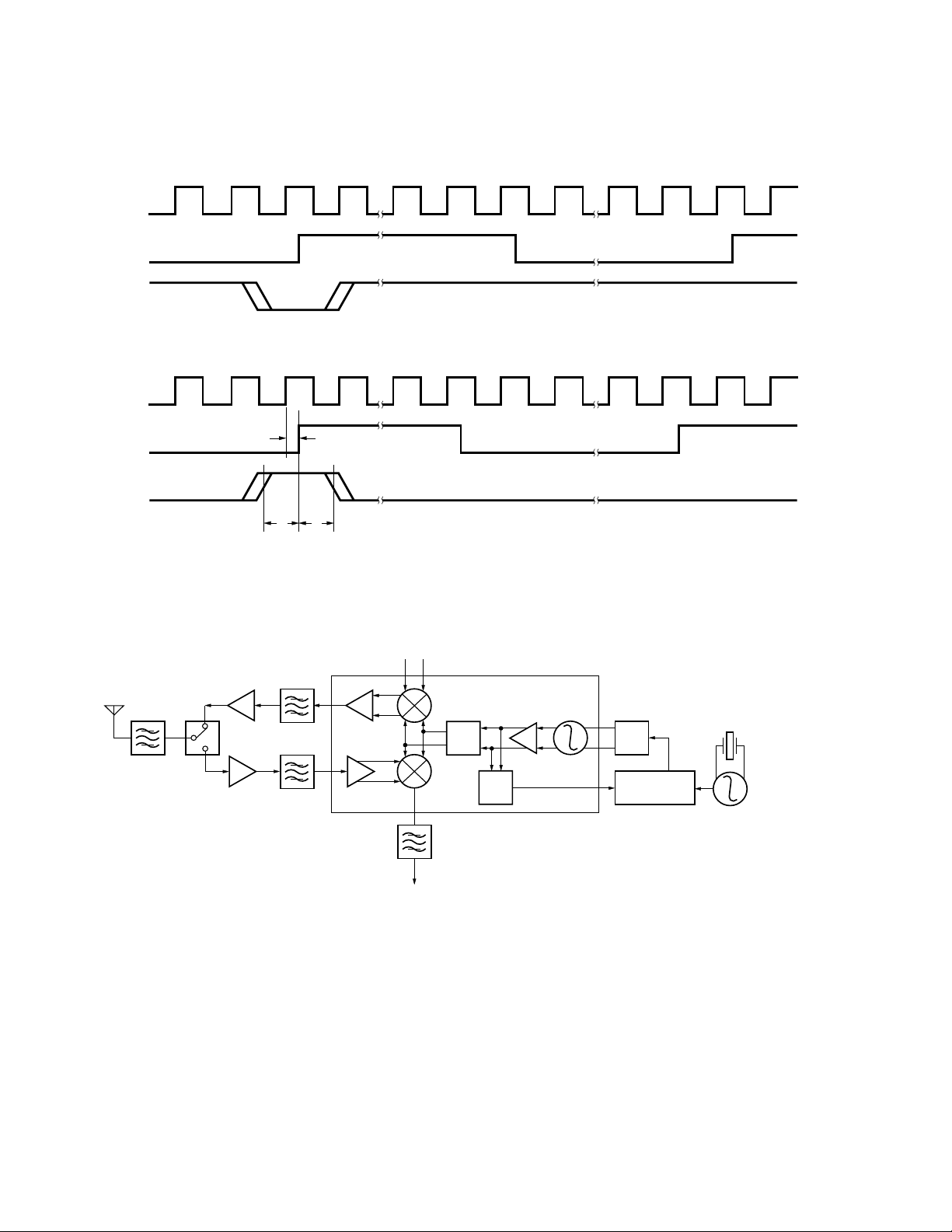
VCO
DIV
31 32 1 2 16 17 18 19 32 33 1 2
DIVMC
31 33 1 2 16 17 18 19 32 1 2 3
VCO
DIV
DIVMC
tpd
ts th
Figure 2. HPMX-5001 Prescaler Timing Diagram.
TX IF INPUT
TX PA
T/R
CERAMIC
TX
FILTER
DIVIDE BY 33 (DIVMC = 0)
DIVIDE BY 32 (DIVMC = 1)
X2
LO1 REFERENCE
TANK
OSCILLATOR
FRONT-END
RF FILTER
RX LNA
CERAMIC
IMAGE
FILTER
HPMX-5001
RX IF FILTER
RX IF OUTPUT
Figure 3. HPMX-5001 Block Diagram/Typical Application.
7-94
32/33
30 MHz
˜
SYNTHESIZER
Page 6

FRONT-END
RF FILTER
TX PA
T/R
RX LNA
CERAMIC
TX.
FILTER
CERAMIC
IMAGE
FILTER
HPMX-5001
IF1 = 110.592 MHz
SAW CHANNEL FILTER
X2
32/33
IF2 = 6.912 MHz
LC FILTER
LC FILTER
CHARGE
PUMP
DATA
FILTER
LO1 ˜ 900 MHz
TANK
30 MHz
˜
SYNTHESIZER
10.368 MHz
REFERENCE
OSCILLATOR
TANK
LO2 = 103.68 MHz
90/216
CHARGE
PUMP
ø FREQ.
DET.
RC FILTER
LC FILTER
RSSI
LOCK
DET.
DATA
SLICER
9/12/16
TX DATA
RX DATA
Figure 4. Typical HPMX-5001 Application with HPMX-5002 IF Chip. All Other Connections Go to Burst Mode Controller,
Power Source, or Ground.
12
10
V
= 5.5 V
CC
8
6
= 3.0 V
V
CC
4
STANDBY MODE (µA)
CC
2
I
V
= 2.7 V
CC
0
-35 -15 25 45
-55 85
5
TEMPERATURE (°C)
48
46
44
VCC = 3.0 V
VCC = 5.5 V
42
40
VCC = 2.7 V
RECEIVE MODE (mA)
CC
38
I
36
-35 -15 25 45
65
-55 85
5
65
TEMPERATURE (°C)
17
16
15
VCC = 5.5 V
VCC = 3.0 V
VCC = 2.7 V
14
SYNTHESIZER MODE (mA)
CC
I
13
-55 85
-35 -15 25 45
5
TEMPERATURE (°C)
65
Figure 5. ICC in Standby Mode vs.
Temperature and VCC.
Figure 6. ICC in Receive Mode vs.
Temperature and VCC.
7-95
Figure 7. ICC in Synthesizer Mode vs.
Temperature and VCC.
Page 7

70
2.0
2.0
VCC = 5.5 V
65
60
TRANSMIT MODE (mA)
CC
I
55
VCC = 3.0 V
VCC = 2.7 V
-55 85
-35 -15 25 45
5
TEMPERATURE (°C)
65
Figure 8. ICC in Transmit Mode vs.
Temperature and VCC.
12
10
8
6
4
2
VCC = 5.5 V
VCC = 2.7 V
1.8
1.6
1.4
5
VCC = 2.7 V
VCC = 5.5 V
65
RXRF VSWR (INPUT)
1.2
1.0
-55 85
-35 -15 25 45
TEMPERATURE (°C)
Figure 9. Receive Downconverter
Input VSWR vs. Temperature and VCC.
0
-5
INPUT IP3
-10
-15
-20
RECEIVE MIXER (dBm)
P1dB
VCC = 2.7 V
VCC = 5.5 V
1.8
1.6
1.4
5
VCC = 2.7 V
VCC = 5.5 V
65
1.2
RXRF VSWR (OUTPUT)
1.0
-35 -15 25 45
-55 85
TEMPERATURE (°C)
Figure 10. Receive Downconverter
Output VSWR vs. Temperature and
VCC.
15.0
14.5
14.0
13.5
13.0
12.5
VCC = 5.5 V
VCC = 2.7 V
0
-35 -15 25 45
-55 85
RECEIVE MIXER SSB NOISE FIGURE (dB)
5
TEMPERATURE (°C)
65
Figure 11. Receive Downconverter
SSB Noise Figure vs. Temperature
and VCC.
0
-10
-20
-30
-40
LEAKAGE (dBm)
LO
-50
2 x f
-60
-70
-55 85
-35 -15 25 45
TEMPERATURE (°C)
VCC = 5.5 V
VCC = 2.7 V
5
65
Figure 14. 2 x fLO Leakage at Receive
Downconverter Output vs.
Temperature and VCC.
-25
-35 -15 25 45
-55 85
5
TEMPERATURE (°C)
65
Figure 12. Receive Downconverter
Input Third Order Intercept Point
and Output 1 dB Compression Point
vs. Temperature and VCC.
40
35
30
25
20
SUPPRESSION (dBc)
LO
15
10
5
0
TRANSMIT 2 x f
VCC = 2.7 V
VCC = 5.5 V
-35 -15 25 45
-55 85
5
TEMPERATURE (°C)
65
Figure 15. 2 x fLO Suppression at
Transmit Upconverter Output vs.
Temperature and VCC.
12.0
-35 -15 25 45
-55 85
RECEIVE MIXER CONVERSION GAIN (dB)
5
TEMPERATURE (°C)
65
Figure 13. Receive Downconverter
Conversion Gain vs. Temperature and
VCC.
3.0
2.6
2.2
1.8
1.4
TXRF VSWR (OUTPUT)
1.0
-35 -15 25 45
-55 85
TEMPERATURE (°C)
VCC = 2.7 V
5
VCC = 5.5 V
65
Figure 16. Transmit Upconverter
Output VSWR vs. Temperature and
VCC.
7-96
Page 8

138.0
137.5
137.0
136.5
136.0
135.5
VCC = 2.7 V
VCC = 5.5 V
3.0
2.0
P
OUT
1.0
0
P1dB
-1.0
TRANSMIT MIXER (dBm)
-2.0
VCC = 2.7 V
VCC = 5.5 V
1.05
1.00
)
p-p
0.95
DIV OUTPUT (V
0.90
VCC = 3.0 V
VCC = 5.5 V
VCC = 2.7 V
135.0
-55 85
TRANSMIT CARRIER TO NOISE RATIO (dB)
-35 -15 25 45
5
TEMPERATURE (°C)
65
Figure 17. Carrier to Noise Ratio at
Transmit Upconverter Output vs.
Temperature and VCC.
DIVV
CC
PIN 26
PIN 28
PIN 27
DIV o/p
DIVGND
-3.0
-55 85
-35 -15 25 45
TEMPERATURE (°C)
Figure 18. Transmit Upconverter
Power Output and Output 1 dB
Compression Point vs. Temperature
and VCC.
RECOMMENDED
OUTPUT CIRCUIT
C = 2.2 nF, R = 51
CR
MAX. LOAD
C = 10 pf, R = 2k
0.85
-35 -15 25 45
5
65
-55 85
5
TEMPERATURE (°C)
65
Figure 19. Prescaler Output Voltage
vs. Temperature and VCC.
Figure 20. Equivalent Circuit and Recommended Output and Load Circuits for
the HPMX-5001 Prescaler Output.
7-97
Page 9

DIVV
PIN 26
CC
DIVMC i/p
LOW = 1/33
OPEN OR V
CC
= 1/32
PIN 30
PIN 27
DIVGND
Figure 21. Equivalent Circuit for the Divider Modulus Control.
VCOV
, PIN 22
CC
TO USE WITH INJECTED LO SIGNAL,
DRIVE PIN 20 (VCOTNKS) WITH
630 m V
LEAVE PIN 21 (VCOTNKF) FLOATING
AS SHOWN BELOW.
C = 22 p MAX. FOR MINIMAL
TURN ON DELAYS.
OPTIONAL
FOR SWR
p-p
.
PIN 20
20
PIN 21
21
7 k
VCOGND, PIN 23
Figure 22. Equivalent Circuit for VCO Tank Connection and Recommended
Tank Circuit.
V
CC
ALL LOGIC CONTROL
PINS ARE ACTIVE LOW.
OPEN OR V
NOT ACTIVE.
TXCTRL, PIN 1
LOCTRL, PIN 31
RXCTRL, PIN 32
CC
=
GND
Figure 23. Equivalent Circuit for Logic Control Pin 1, 31, and 32.
7-98
Page 10

RXRF
50 Ω i/p
TXRX V
2.7 pF
LNAREF
CC
10
BIAS
TO MIXER
8
7
BIAS
3.3 pF
PCB GND
11
15
ARE FOR TYPICAL i/p SWR
LNA STAGE
TXRX GND
Figure 24. Equivalent Circuit for RXRF Input.
TXRX V
CC
TXIF 5
TXIFB 6
11/15
10
10 k 10 k
TX i/p STAGE
RECOMMENDED DRIVE
LEVEL IS 300 mV pk-pk.
TXIF IN
USE d.c. BLOCKING Cs TO
AVOID CHANGING d.c. BIAS
CONDITIONS. 22 pF MAX. FOR
QUICK TURN ON.
TXRX GND
Figure 25. Equivalent Circuit for TXIF Input.
EXTERNAL COMPONENTS
OF 1.3:1 OVER 1.85
TO 2.55 GHz
V
CC
LO
RF
750
3 RXIFB
120 nH
4 RXIF
EXTERNAL COMPONENTS
SHOWN ARE FOR 110.592 MHz
I.F. AND TYPICAL 50 Ω o/p
SWR OF 1.3:1
11/15
TXRX GND
6.8 pF
8.2 pF
50 Ω o/p
Figure 26. Equivalent Circuit for the RXIF Output and Recommended Matching
Circuit for 110.592 MHz IF.
7-99
Page 11

S
V
CC
3.3 nH 50
12
TX o/p STAGE
TXRFB
14
TXRF
11/15
TXRX GND
300
EXAMPLE o/p NETWORK FOR
OTHER SYMMETRIC NETWORKS
WILL ENABLE OPERATION
3.3 nH
50 Ω o/p
22 pF
1.88–1.90 GHz.
UP TO 2.50 GHz.
Figure 27. Equivalent Circuit for TXRF Output and Matching Network for
DECT Phone Operation.
P9
P8
P7
RXIF
TXIF
P1
C2
R8
R9
P10
R10
C13
C1
T1
RXRF
L1
C3
C4
C6
V
CC
C12
1
R1
C5
8
C11
32
9
R7
C10
C9
R5
+ 32/33
X2
25
24
R4
R6
C8
17
16
VCOTNK
Ground
R2
X3
L3L2
C7
TXRF
Figure 28. Test Board Schematic Diagram. All I/O Labels Correspond to Those on the Test board. See Table 3 for
Component Values.
7-100
Page 12

Table 3. Test Board Components Shown in Figure 28.
Note: Required VCC decoupling capacitors are not shown on the
schematic. Detailed schematic and board layout are available in
Application Note 1081.
Component Label Value (Size)
R1 270 (0805)
R2, R4, R5 51.1 (0805)
X3 R = 300 (0805) for 1.89 GHz,
L = 3.3 nH for 2.45 GHz
R6 20 (0805)
R7, R8, R9, R10 1100 (0805)
C1 see Table 4
C2 see Table 4
C3, C4, C10, C11, C12, C13 1 nF (0805 or 0504)
C5 3.3 pF (0504 or 0603)
C6 2.7 pF (0805)
C7 22 pF (0805) for 1.89 GHz,
3.3 pF for 2.45 GHz
C8 12 pF (0805 or 0504)
C9 2.2 nF (0805)
L1 see Table 4
L2, L3 3.3 nH (0805)
T1 1:4 Balun T4-1-X65
Table 4. Component changes for dfferent IF frequencies.
Functional Description
A typical DECT application of the
HPMX-5001 in a dual-conversion
superheterodyne radio transceiver is shown in Figure 3. The
HPMX-5001 is designed to
provide four different modes of
operation:
• Transmit, where the VCO,
doubler, upconverting mixer,
associated buffers, and
prescaler are enabled
• Receive, where the VCO,
doubler, downconverting
mixer, associated buffers, and
prescaler are enabled
• Synthesizer, where only the
VCO and prescaler are active
• Standby, where all circuits are
disabled
These four modes are controlled
via a three wire interface,
TXCTRL, RXCTRL, and LOCTRL.
Figure 1 shows the programming
logic states for all four modes.
The detailed description of the
three active modes is given
below.
IF Frequency C1, pF C2, pF L1, nH VSWR
110 MHz 6.8 8.2 120 1.3:1
200 MHz 1.0 3.9 100 1.3:1
250 MHz 1.2 3.9 56 1.3:1
300 MHz 1.2 3.9 39 1.3:1
350 MHz 2.7 2.7 27 1.3:1
7-101
Page 13

Transmit Mode
For transmit upconversion, a
differential narrow-band
modulated signal is AC-coupled
into the TXIF and TXIFB inputs.
The differential signal may be
generated by the HPMX-5002 IF
Demodulator/Modulator. Once
on-chip, the signal is buffered and
applied to a double-balanced
Gilbert cell mixer. The
upconverted RF signal is then
amplified to generate a -0.6 dBm
single-ended, single-sideband
power signal at the 1 dB
compression point. The RF
outputs, TXRF and TXRFB, are
open-collector outputs (see test
diagram Figure 28 for recommended matching network). The
TXRF output is AC-coupled into a
50 Ω transmit filter. This signal is
then filtered and amplified offchip by an external power amplifier before it is switched into the
antenna. The HPMX-5001 may
also be used in DECT systems
which utilize direct modulation of
the 1LO for data transmission. In
this case, either the TXIF or
TXIFB input, but not both, must
be tied to VCC to cause the
upconverting mixer to act as a
buffer stage.
Receive Mode
In receive mode, a preamplified
RF signal is passed through an
image filter and applied as a
single-ended signal to the 50 Ω
RXRF input. Use of a 2.7 pF
blocking capacitor is recommended. RXRF is the noninverting input of the RF input
amplifier. The inverting input of
this amplifier, LNAREF, is selfbiased and requires only an
external capacitor (recommended
value of 3.3 pF) to ground. The
receive downconversion mixer
also employs a double-balanced
Gilbert cell configuration. The
production version of the
HPMX-5001 will have two
equivalent open collector outputs.
The HPMX-5001 can operate at IF
frequencies up to 300 MHz (see
Figure 28 for recommended
matching network).
Synthesizer Mode
The on-chip 32/33 dual-modulus
prescaler, in conjunction with the
VCO, external tank circuit, and
CMOS synthesizer, form a phaselocked loop (PLL). The prescaler
divider output and modulus
control input are designed to be
compatible with positive-edge
triggered CMOS synthesizers
from a variety of vendors. The
timing requirements for the
prescaler are shown in Figure 2.
It is important to note that the
prescaler divides the VCO signal,
and not the frequency doubler
output. Local oscillator (LO)
signal generation on the
HPMX-5001 is accomplished
through the combination of a
VCO and frequency doubler. The
VCO is a simple Clapp oscillator
for the best possible noise
performance. The VCO force and
sense pins (VCOTNKF,
VCOTNKS) are self-biased, so
that the connections to the tank
(minimum Q of 20) are through
AC-coupling capacitors.
VCOTNKS can also be used with
an injected LO. VCOTNKF would
then be left floating. The doubler
circuit multiplies the VCO
frequency by two. This enables
the VCO to have lower sensitivity
to both package parasitics and LO
re-radiation. Separate bias pins
and buffering are utilized to
minimize pulling of the VCO
when the chip is switched from
synthesizer to transmit or receive
mode.
7-102
Page 14

Part Number Ordering Information
Part Number No. of Devices Container
HPMX-5001-STR 10 Strip
HPMX-5001-TR1 1000 Tape and Reel
HPMX-5001-TY1 250 Tray
Package Dimensions 32 Pin Thin Quad Flat Package
All dimensions shown in mm.
9.0 ± 0.25
7.0 ± 0.1
9.0 ± 0.25
HPMX-5001
YYWW
XXXX ZZZ
7.0 ± 0.1
0.6
0.35
TYP.
+ 0.15
- 0.10
0.8
1.4 ± 0.05
0.05 MIN., 0.1 MAX.
7-103
Page 15

Tape Dimensions and Product Orientation for Outline TQFP-32
REEL
CARRIER
TAPE
USER
FEED
DIRECTION
COVER TAPE
0.30 ± 0.05
2.0 (See Note 7)
4.0 (See Note 2)
1.5+0.1/-0.0 DIA
1.75
R 0.5 (2)
5.0
1.6 (2)
B
O
K
1
K
O
6.4 (2)
A
O
12.0
HPMX-5001
7.5 (See Note 7)
1.5 Min.
Cover tape width = 13.3 ± 0.1 mm
Cover tape thickness = 0.051 mm (0.002 inch)
NOTES:
AO = 9.3 mm
B
= 9.3 mm
O
K
= 2.2 mm
O
K
= 1.6 mm
1
1. Dimensions are in millimeters
2. 10 sprocket hole pitch cumulative tolerance ±0.2
3. Chamber not to exceed 1 mm in 100 mm
4. Material: black conductive Advantek™ polystyrene
5. A
and BO measured on a plane 0.3 mm above the bottom of the pocket.
O
6. K
measured from a plane on the inside bottom of the pocket to the top surface of the carrier.
O
7. Pocket position relative to sprocket hole measured as true position of pocket, not pocket hole.
16.0 ± 0.3
7-104
 Loading...