

Page 1
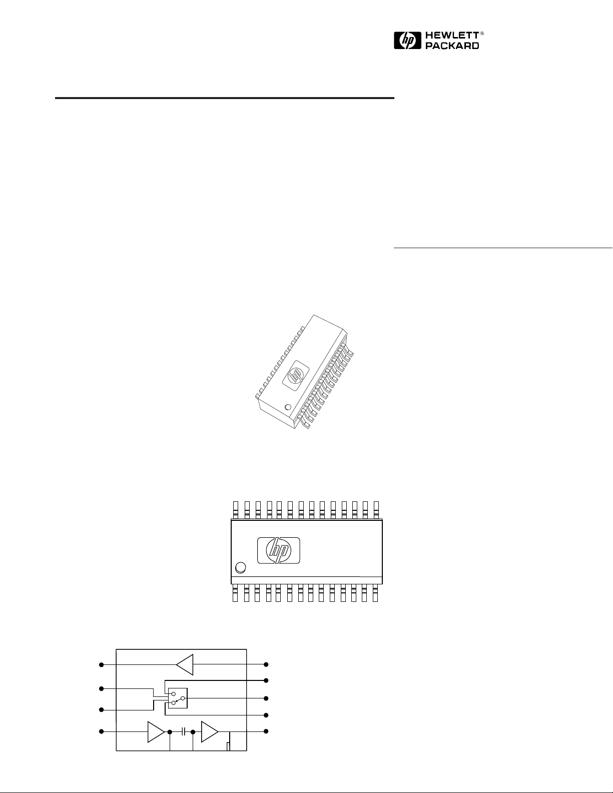
1.5 – 2.5 GHz LNA Switch PA
Technical Data
HPMX-3003
Features
• GaAs MMIC LNA-SwitchPower Amp for 1.5 – 2.5 GHz
Transceiver Use
• LNA: 2.2 dB NF, 13 dB Ga @
1.9 GHz
• Switch: 55 dBm OIP @
1.9␣ GHz
• Power Amp: +4 dBm in,
+27.5 dBm out, 23.5 dB Gain,
35% η
@ 1.9 GHz
add
• 3 or 5 V Operation
• JEDEC Standard SSOP-28
Surface Mount Package
Applications
• Personal Communications
Systems (PCS)
• Cordless Telephone Systems
• 2400 MHz Wireless LANs
and ISM Band Spread
Spectrum Applications
Functional Block Diagram
LNA out
C1
C2
(VG1)
Plastic SSOP-28
HPMX
3003
Package Pin Configuration
25 PA out
24 Gnd
23 Gnd
22 PA out
Gnd 6
VD1 7
21 PA out
LNA out 8
VD2VD1 VG2
28 Gn
Gnd 1
27 VG2
26 Gnd
Gnd 2
Gnd 3
Gnd 5
PA in 4
LNA in
SW1
Antenna
SW2
PA outPA in
YYWW
20 Gnd
19 Gnd
18 SW2
HPMX
3003
YYWW
Gnd 9
Gnd 10
LNA in 11
17 Gnd
16 C2
Gnd 12
SW1 13
Description
Hewlett-Packard’s HPMX-3003
combines a Low Noise Amplifier,
GaAs MMIC switch, and 27.5 dBm
power amp in a single miniature
28 lead surface mount plastic
package. This RFIC would
typically serve as the “front end”
and power stage of a battery
operated wireless transceiver for
PCS or ISM band use. Each
section of the RFIC can also be
used independently.
The single-supply LNA makes use
of the low noise characteristics of
15 Antenna
GaAs to create a matched, broadband amplifier with target performance of 13 dB gain and 2.2 dB
noise figure. The switch provides
+55 dBm IP3 for linear operation.
The power amplifier produces up
to 820␣ mW with 35% power added
efficiency.
The HPMX-3003 is fabricated with
Hewlett-Packard’s GaAs MMIC
C1 14
process, and features a nominal
0.5 micron recessed Schottkybarrier-gate, gold metallization,
and silicon nitride passivation to
produce MMICs with superior
performance, uniformity and
reliability.
5965-1403E
7-82
Page 2
HPMX-3003 Absolute Maximum Ratings
[1]
Absolute Absolute Absolute
Symbol Parameter Units Maximum
LNA Switch Power Amp
P
diss
P
in
V
d
V
cont
T
ch
T
STG
Notes:
1. Operation of this device above any of these limits may cause permanent
damage.
case
= 25°C
2. T
3. Derate at 18.2 mW/° C for T
Power Dissipation
CW RF Input Power dBm +20 +33 +20
Device Voltage V 8 — 8
Control Voltage V — -6 —
Channel Temperature °C 175 175 175
Storage Temperature °C -65 to 150 -65 to 150 -65 to 150
> 78°C
C
[2,3]
mW 250
[2,3]
[1]
Maximum
[1]
Thermal Resistance
θjc = 55°C/W
Maximum
[2,3]
1500
[2]
[1]
:
Recommended operating range of Vcc = 2.7 to 5.5 V, T
= -40 to + 85 ° C
a
HPMX-3003 Standard Test Conditions
Unless otherwise stated, all test data was taken on packaged parts
under the following conditions:
T
= 25 ° C, Zo = 50 Ω
a
Vcc = +3.0 V DC, V
= -3.0 V DC, VD1 = +3.6 V DC
control
LNA Pin = -20 dBm, PA Pin = +4 dBm, frequency = 1.9 GHz
Perfomance cited is performance in test circuit shown in Figure 17.
HPMX-3003 Guaranteed Electrical Specifications
Standard test conditions apply unless otherwise noted.
Symbol Parameters and Test Conditions Units Min. Typ. Max.
G
test
P
out
Id LNA LNA bias current mA 6.5 9.5
LNA gain through switch dB 9.0 11
Output power through switch dBm 24.0 25.5
7-83
Page 3
HPMX-3003 Summary Characterization Information
Standard test conditions apply unless otherwise noted. All information tested in 1900 MHz
Test Circuit, and reflects performance of test circuit at 1900 MHz.
Symbol Parameters and Test Conditions Units Typ
LNA
NF Noise Figure dB 2.2
2
|S21|
IRL Input Return Loss dB 15
ORL Output Return Loss 12
IIP
Switch
P
1dB
where insertion loss is increased by 1 dB
P
1dB
where insertion loss is increased by 1 dB
IP
3
S21 on Insertion Loss, on channel dB 0.8
S21 off Isolation, off channel dB 15
IRL
IRL
off
Power amp (Vg = -.8 V required)
GP Gain VD1 = 3.6 V, Pin = + 4 d Bm d B 23.5
η
PA
add
P
out
Id PA Transmit Current VD1 = 3.6 V, Pin = +4 dBm mA 450
Note:
1. The P
C2 from the normal 3 V (+23 dB P
50 Ω Gain dB 13
Input Third Order Intercept dBm -1
3
Output Power ∆C1 to C2 = 3 V dBm +23
Output Power ∆C1 to C2 = 5 V dBm +29
[1]
Third Order Intercept dBm +55
on
Return Loss, on channel dB 26
Return Loss, off channel dB 0.5
Power Added Efficiency VD1 = 3.6 V % 35
Output Power VD1 = 3.6 V, Pin = + 4 d B m dB m +27.5
of the switch can be improved by increasing the difference between the values of C1 and
1dB
) to 5 V (+29 dB P
1dB
1dB
).
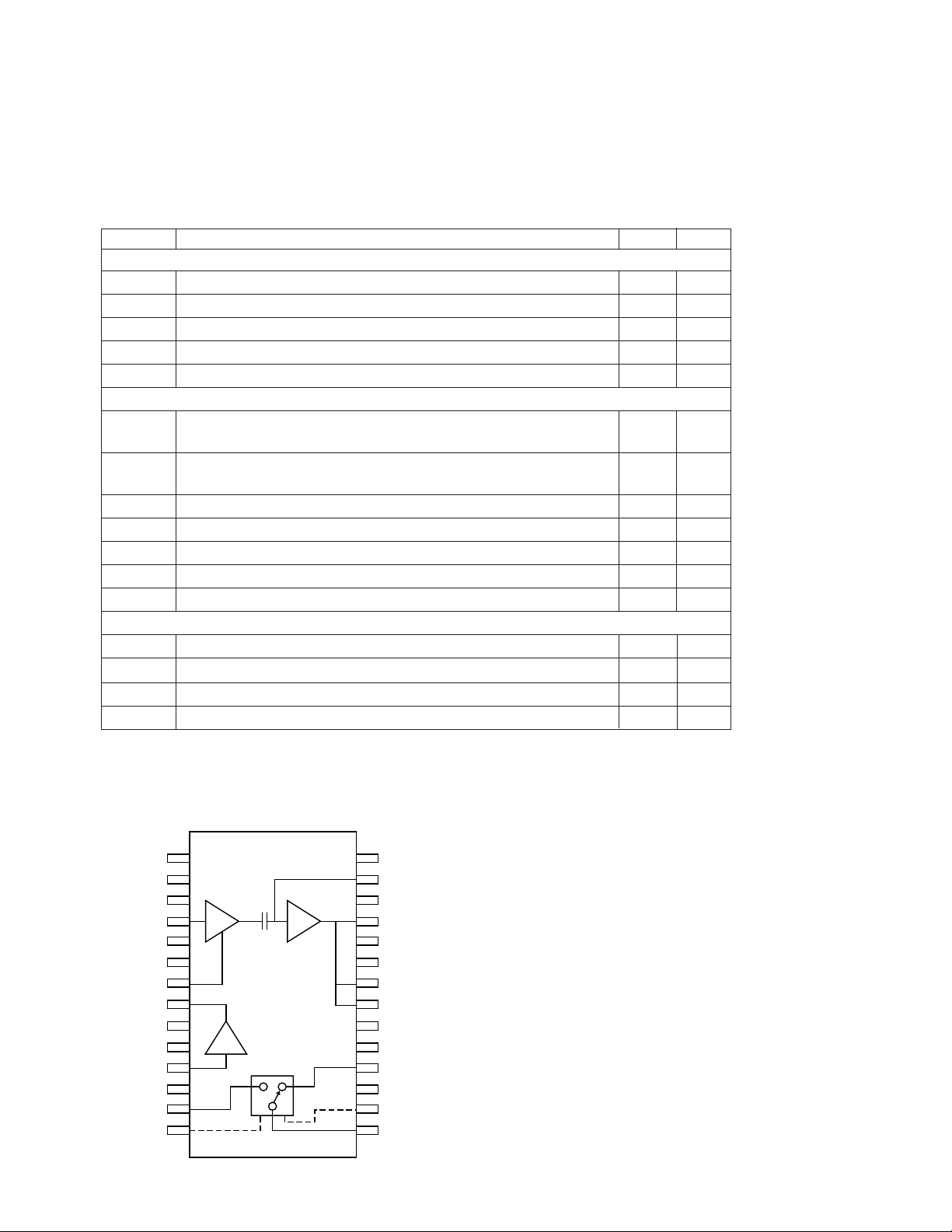
HPMX-3003 Pin Description
Gnd 1
Gnd 2
Gnd 3
PA in 4
Gnd 5
Gnd 6
VD1 7
LNA out 8
Gnd 9
Gnd 10
LNA in 11
Gnd 12
SW1 13
C1 14
Figure 1. HPMX-3003 Pin Outs and Schematic.
28 Gn
27 VG2
26 Gnd
25 PA out
24 Gnd
23 Gnd
22 PA out
21 PA out
20 Gnd
19 Gnd
18 SW2
17 Gnd
16 C2
15 Antenna
7-84
Page 4

HPMX-3003 Pin Description Table
No. Mnemonic Description Typical Signal Description
1 Gnd ground 0 V Short path with minimal parasitics. Ground pins are
2 Gnd ground 0 V also the primary thermal path for heatsinking the device.
3 Gnd ground 0 V
4PA
5 Gnd ground 0 V Short path with minimal parasitics. Ground pins are also
6 Gnd ground 0 V the primary thermal path for heatsinking the device.
7 VD1 Drain bias +3 V, 100 mA Set drain bias to 3 V (can be tied to same rail as PA out).
8 LNA out output of LNA DC: +3 V, 5 mA Bias through 5 nH choke (printed on PC board) and 100 pF
9 Gnd ground 0 V Short path with minimal parasitics. Ground pins are also
10 Gnd ground 0 V the primary thermal path for heatsinking the device.
11 LNA in input of LNA DC: 0 V 50 Ω transmission line from switch. Input blocking capacitor
12 Gnd ground 0 V Short path with minimal parasitics. Ground pins are also
13 SW1 switch DC: 0 V Switch input or output. Symmetrical with SW2. 50 Ω
14 C1 switch control 1 closed: 0 V High impedance line to control switch, used in conjunction
15 Antenna switch center DC: 0 V 50 Ω transmisson line to/from antenna. Line should not
16 C2 switch control 2 closed: 0 V High impedance line to control switch, used in conjunction
17 Gnd ground 0 V Short path with minimal parasitics. Ground pins are also the
18 SW2 switch DC: 0 V Switch input or output. Symmetrical with SW1. 50 Ω
19 Gnd ground 0 V Short path with minimal parasitics. Ground pins are also
20 Gnd ground 0 V the primary thermal path for heatsinking the device.
21 PA out output of PA DC: 3 V, 350 mA 2.7 pF chip capacitor to ground provides 1.9 GHz output
22 PA out output of PA RF: +27 dBm match for PA. 50 Ω transmission line to switch. LC choke
23 Gnd ground 0 V Short path with minimal parasitics. Ground pins are also
24 Gnd ground 0 V the primary thermal path for heatsinking the device.
25 PA out output of PA DC: 3 V, 350 mA Leave unconnected; use pins 21 & 22 for PA out.
26 Gnd ground 0 V Short path with minimal parasitics. Ground pins are also
27 VG2 Gate bias on -0.75 V Provide bias through 10 Ω resistor. Bypass to ground at pin
28 Gnd ground 0V Short path with minimal parasitics. Ground pins are also the
input to Power DC: -0.75 V Bias through 500 Ω resistor and 100 pF capacitor. 50 Ω trans-
in
Amplifier RF: +4 dBm mission line with DC blocking capacitor (>24 pF) to input.
Shunt 2.7 pF used on test board to match input at 1.9 GHz.
of PA stage 1 Bypass with 100 pF capacitor at pin.
RF: -7 dBm bypass capacitor to 10 Ω resistor and 1000 pF bypass
capacitor. Can be operated from 3 to 5 V supply line. 50 Ω
transmission line with DC block (>24 pF) to receiver.
RF: -20 dBm (24 pF) and shunt 5 nH inductor to ground (noise match at
1.9 GHz) required. Typically a filter is employed between the
LNA input and the switch.
the primary thermal path for heatsinking the device.
terminal 1 RF: -20 dBm transmission line to LNA (or PA). Line should not carry
DC voltage.
open: -3 to -5 V with C2. C2 should be open when C1 is closed.
pole RF: +26 dBm carry DC voltage.
open: -3 to -5 V with C1. C1 should be open when C2 is closed.
primary thermal path for heatsinking the device.
terminal 2 RF: +4 dBm transmission line to PA (or LNA). Line should not carry
DC voltage.
and blocking C used. Typically a filter is employed between
the PA output and the switch input.
RF: +27 dBm
the primary thermal path for heatsinking the device.
PA stage 2 with 10 pF capacitor, and on power supply side of resistor
with 1000␣ pF capacitor.
primary thermal path for heatsinking the device.
7-85
Page 5

HPMX-3003 Typical Performance
Standard test conditions apply unless otherwise noted. 2.4 GHz performance is performance in test circuit
shown in Figure 18. Some aspects of performance are determined by the test circuit impedances.
10
9
8
7
6
(mA)
5
4
CURRENT
3
2
1
0
2.5 4 4.5 53 3.5 5.5 6 2.5 4 4.5 53 3.5 5.5 6
VOLTAGE (V)
Figure 2. LNA Current vs. Device
Voltage at 1900 MHz.
20
15
(dB)
10
GAIN
5
0
VOLTAGE (V)
2400 MHz
1900 MHz
Figure 3. LNA Gain vs. Device Voltage
and Frequency.
5
4
(dB)
3
2
NOISE FIGURE
1
0
2.5 4 4.5 53 3.5 5.5 6
VOLTAGE (V)
2400 MHz
1900 MHz
Figure 4. LNA Noise Figure vs. Device
Voltage and Frequency.
8
7
6
5
(mA)
4
3
CURRENT
2
1
0
-60 0 20 40-40 -20 60 80 100
TEMPERATURE (°C)
Figure 5. LNA Current vs.
Temperature at 1900 MHz.
12
10
(mA)
8
6
CURRENT
4
2
2.5 4 4.5 53 3.5 5.5 6
VOLTAGE (V)
Figure 8. PA Current vs. Device
Voltage at 1900 MHz.
Stg 2
Stg 1
20
15
(dB)
10
GAIN
5
0
-60 0 20 40-40 -20 60 80 100
TEMPERATURE (°C)
Figure 6. LNA Gain vs. Temperature
at 1900 MHz.
35
30
25
20
(dBm)
15
Pout
10
5
0
2.5 4 4.5 53 3.5 5.5 6
VOLTAGE (V)
1900 MHz
2400 MHz
Figure 9. PA Output Power vs. Supply
Voltage and Frequency.
5
4
(dB)
3
2
NOISE FIGURE
1
0
-60 0 20 40-40 -20 60 80 100
TEMPERATURE (°C)
Figure 7. LNA Noise Figure vs.
Temperature at 1900 MHz.
50
40
1900 MHz
30
(%)
PAE
20
2400 MHz
10
0
2.5 4 4.5 53 3.5 5.5 6
VOLTAGE (V)
Figure 10. PA Power Added Efficiency
vs. Supply Voltage and Frequency.
7-86
Page 6

HPMX-3003 Typical Performance, continued
Standard test conditions apply unless otherwise noted. 2.4 GHz performance is performance in test circuit
shown in Figure 18. Some aspects of performance are determined by the test circuit impedances.
400
350
300
250
200
CURRENT (mA)
150
100
50
-60 0 20 40-40 -20 60 80 100
TEMPERATURE (°C)
Figure 11. PA Current vs.
Temperature at 1900 MHz and
VD1 = 3.6V.
Stg 2
Stg 1
35
30
25
20
15
POWER (dBm)
10
5
0
-60 0 20 40-40 -20 60 80 100
TEMPERATURE (°C)
Figure 12. PA Output Power vs.
Temperature at 1900 MHz and
VD1 = 3.6V.
50
40
30
PAE (%)
20
10
0
-60 0 20 40-40 -20 60 80 100
TEMPERATURE (°C)
Figure 13. PA Power Added Efficiency
vs. Temperature at 1900 MHz and
VD1 = 3.6V.
0
-10
-20
ISOLATION/R.L. (dB)
-30
-40
1.4 2.0 2.2 2.41.6 1.8 2.6
FREQUENCY (GHz)
Figure 14. Switch Isolation and “ON”
State Return Loss vs. Frequency.
0
-1
-2
R.L. (dB)
-3
-4
-5
1.4 2.0 2.2 2.41.6 1.8 2.6
FREQUENCY (GHZ)
Figure 15. Switch “OFF” State Return
Loss vs. Frequency.
0
-1
-2
I.L. (dB)
-3
-4
-5
1.4 2.0 2.2 2.41.6 1.8 2.6
FREQUENCY (GHZ)
Figure 16. Switch “ON” State
Insertion Loss vs. Frequency.
HPMX-3003 Typical Scattering Parameters for the LNA,
Common Source, Z
Frequency S
GHz Mag Ang Mag Ang Mag Ang Mag Ang
1.0 0.97 -27 2.00 158 0.035 -12 0.91 -22
1.2 0.96 -33 2.06 150 0.036 -17 0.91 -27
1.4 0.95 -40 2.13 142 0.037 -23 0.90 -31
1.6 0.94 -47 2.20 134 0.038 -30 0.88 -36
1.8 0.92 -54 2.28 125 0.038 -39 0.87 -41
2.0 0.90 -62 2.36 117 0.039 -49 0.86 -46
2.2 0.88 -70 2.45 109 0.039 -62 0.84 -50
2.4 0.85 -79 2.54 100 0.040 -77 0.83 -55
2.6 0.82 -89 2.63 90 0.042 -95 0.81 -60
2.8 0.78 -99 2.71 81 0.045 -115 0.79 -65
3.0 0.75 -110 2.79 71 0.050 -135 0.78 -71
= 50 Ω, V
O
= 3 V, ID = 5 mA
D
11
S
21
S
12
S
22
7-87
Page 7

PA in
100 pF
~
– 0.75V
VG1
VD1 = 3.6V
LNA out
3.0V
30 pF
2.7 pF
500
100 pF
30 pF
10
100 pF1000 pF
5 nH
10 pF
30 pF
10
SW2
1000 pF
18 nH2.7 pF
30 pF
VG2
~
– 0.75V
VD2 = 3.6V
PA out
LNA in
SW1
C1
Figure 17. HPMX-3003 Test Circuit (1900 MHz).
PA in
100 pF
~
– 0.75V
VG1
VD1 = 3.6V
LNA out
3.0V
LNA in
30 pF
1.5 pF
500
100 pF
30 pF
2.5 nH
10
100 pF1000 pF
2.5 nH
5 nH
10 pF
30 pF
C2
10
SW2
C2
Antenna
1000 pF
18 nH1.5 pF
30 pF
VG2
~
– 0.75V
VD2 = 3.6V
PA out
SW1
C1
Figure 18. HPMX-3003 Test Circuit (2400 MHz).
Antenna
7-88
Page 8

JEDEC Standard SSOP-28 Package Outline Drawing
8.255 (0.325)
6.000 (0.236)
3.850 (0.152)
10.000 (0.394)
1.400 (0.055)
TYPICAL DIMENSIONS ARE
IN MILLIMETERS (INCHES)
MEETS JEDEC
OUTLINE DIMENSIONS
0.635 (0.025)
0.185 (0.007)
0.250 (0.010)
Part Number Ordering Information
Part Number No. of Devices Container
HPMX-3003-TR1 1000 Tape and Reel
HPMX-3003-BLK 25 Tape
0.600 (0.024)
7-89
 Loading...