

Page 1
7-54
Silicon Bipolar RFIC 100 MHz
Vector Modulator
Technical Data
Features
• 25 - 250 MHz Output
Frequency
• -5 dBm Peak P
out
• Unbalanced 50 Ω Ouptut
Match
• Internal 90° Phase Shifter
• 5 V, 15 mA Bias
• SO-16 Surface Mount
Package
Applications
• Dual Conversion Cellular
Telephone and PCS
Handsets
• Dual Conversion ISM Band
Transmitters and LANs
• Direct Conversion Digital
Transmitters for 25- 250␣ MHz
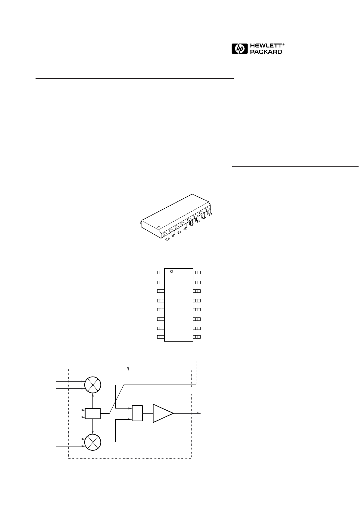
Functional Block Diagram
Plastic SO-16 Package
Pin Configuration
Description
Hewlett Packard’s HPMX-2005 is a
silicon RFIC vector modulator
housed in a SO-16 surface mount
plastic package. This IC can be
used for direct modulation at output frequencies from 25 to
250␣ MHz, or, in combination with
an up-converting mixer, for dual
or multiple conversion modulation to higher frequencies. The IC
contains two matched Gilbert cell
mixers, an RC phase shifter, a
summer, and an output amplifier.
This RFIC is well suited to portable and mobile cellular telephone applications such as North
American Digital Cellular, GSM,
and Japan Digital Cellular, and to
Personal Communications Systems such as DCS-1800 or
handyphones. It is also useful for
applications in 900 MHz, 2.4 GHz
and 5.7 GHz ISM (Industrial-Scientific-Medical) bands requiring digital modulation, such as Local Area
Networks (LANs).
The HPMX-2005 is fabricated with
Hewlett-Packard’s 25 GHz
ISOSAT-II process, which combines stepper lithography, selfalignment, ion-implantation
techniques, and gold metallization
to produce state of the art RFICs.
HPMX-2005
OUTPUT
AMPLIFIER
I
ref
Q MIXER
0°
V
CC
RF
out
50 Ω Z
o
(UNBALANCED)
I MIXER
I
mod
LO +
Q
mod
Q
ref
90°
LO –
φ ADJUST
(OPTIONAL CONNECTION FOR
OPERATION AT 140-250 MHz)
φ
SUMMER
Σ
PHASE
SHIFTER
16 V
CC
15 RF
out
14 GROUND
13 GROUND
12 I
ref
11 I
mod
10 GROUND
9 φ ADJUST
V
CC
1
V
CC
2
GROUND 3
GROUND 4
Q
mod
6
LO +
7
LO –
8
Q
ref
5
5965-9104E
Page 2
7-55
HPMX-2005 Guaranteed Electrical Specifications, T
A
= 25° C, ZO = 50 Ω
VCC = 5 V, LO = -12 dBm @ 100 MHz (Unbalanced Input), V
Iref
= V
Qref
= 2.5 V (unless otherwise noted).
Symbol Parameters and Test Conditions Units Min. Typ. Max.
I
d
Device Current mA 14 17
P
out
Output Power V
Imod
= V
Qmod
= 3.25 V dBm -7 -5
LO
leak
P
out
- LO at Output V
Imod
= V
Qmod
= 2.5 V dBc 30 36
ε
mod
Average % 2.5 5
Modulation
Error
HPMX-2005 Absolute Maximum Ratings, T
A
= 25° C
Absolute
Symbol Parameter Units Maximum
[1]
P
diss
Power Dissipation
[2,3]
mW 500
LO
in
LO Input Power dBm 15
V
CC
Supply Voltage V 10
[4]
∆V
Imod
, Swing of V
Imod
about V
Iref
or V
p-p
5
[4]
∆V
Qmod
V
Qmod
about V
Qref
V
Iref
, V
Qref
Reference Input Levels V 5
T
STG
Storage Temperature °C -65 to 150
T
j
Junction Temperature °C 150
Thermal Resistance
[2]
:
θjc = 125°C/W
Notes:
1. Operation of this device above any one
of these parameters may cause
permanent damage.
2. TC = 25°C (TC is defined to be the
temperature at the ends of pin 3 where
it contacts the circuit board).
3. Derate at 8 mW/°C for TC > 87°C.
4. This voltage must not exceed V
CC
by
more than 0.8 V.
HPMX-2005 Summary Characterization Information. T
A
= 25° C, ZO = 50 Ω
VCC = 5 V, LO = -12 dBm @ 100 MHz (Unbalanced Input), V
Iref
= V
Qref
= 2.5 V (unless otherwise noted).
Symbol Parameters and Test Conditions Units Typ.
R
in
Input Resistance (I
mod
to I
ref
or Q
mod
to Q
ref
) Ω 10 k
R
in-gnd
Input Resistance to Ground (Any I, Q Input to Ground) Ω 10 k
VSWR
LO
LO VSWR (50 Ω) 25 - 200 MHz Bandwidth 1.5:1
VSWR
O
Output VSWR (50 Ω) 25 - 200 MHz Bandwidth 2.5:1
- Output Noise Floor V
Imod
= V
Qmod
= 3.25 V dBm/Hz -134
IM
3
DSB Third Order Intermodulation Products dBc 33
A
i
RMS Amplitude Error dB 0.15
P
i
RMS Phase Error degrees 1.0
√(V
Imod
- 2.5)2 + (V
Qmod
- 2.5)2 = 0.75 V
Page 3
7-56
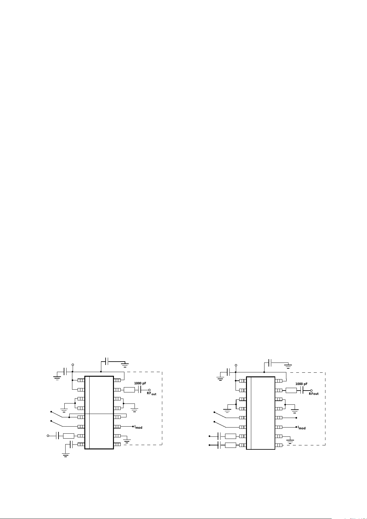
Figure 1. HPMX-2005 Connections Showing Unbalanced
LO and I/Q Inputs.
Figure 2. HPMX-2005 Connections Showing Differential
LO and I/Q Inputs.
HPMX-2005 Pin
Descriptions
VCC (pins 1, 2 & 16)
These three pins provide DC
power to the RFIC, and are connected together internal to the
package. They should be connected to a 5 V supply, with appropriate AC bypassing (1000 pF
typ.) used near the pins, as shown
in figures 1 and 2.The voltage on
these pins should always be
kept at least 0.8 V more posi-
tive than the DC level on any
of pins 5, 6, 11, or 12. Failure to
do so may result in the modulator
drawing sufficient current
through the data or reference inputs to damage the IC (see also
Figure 5).
Ground (pins 3, 4, 10, 13 & 14)
These pins should connect with
minimal inductance to a solid
ground plane (usually the backside of the PC board). Recommended assembly employs
multiple plated through via holes
where these leads contact the PC
board.
I
ref
(pin 12) and Q
ref
(pin 5)
I
mod
(pin 11) and Q
mod
(pin 6)
Inputs
The I and Q inputs are designed
for unbalanced operation but can
be driven differentially with similar performance. The recommended level of unbalanced I and
Q signals is 1.5 V
p-p
with an average level of 2.5 V above ground.
The reference pins should be DC
biased to this average data signal
level (VCC/2 or 2.5 V typ.). For
single ended drive, pins 5 and 12
can be tied together. For differential operation, 0.75 V
p-p
signals
may be applied across the I
mod/Iref
and the Q
mod/Qref
pairs. The average level of all four signals should
be about 2.5 V above ground. The
impedance between Iin or Qin and
ground is typically 10 kΩ and the
impedance between I
mod
and I
ref
or Q
mod
and Q
ref
is typically
10␣ k Ω. The input bandwidth typically exceeds 40 MHz. It is possible to reduce LO leakage
through the IC by applying slight
DC imbalances between I
mod
and
I
ref
and/or Q
mod
and Q
ref
(see page
9). All performance data shown
on this data sheet was taken with
unbalanced I/Q inputs.
LO Input (pins 7 and 8)
The LO input of the HPMX-2005 is
balanced (differential) and
matched to 50 Ω. For drive from a
unbalanced LO, pin 7 should be
AC coupled to the LO using a 50 Ω
transmission line and a blocking
capacitor (1000 pF typ.), and pin 8
should be AC grounded (1000 pF
capactitor typ.), as shown in figure 1. For drive from a differential
LO source, 50 Ω transmission
lines and blocking capacitors
(1000 pF typ.) are used on both
pins 7 and 8, as shown in figure 2.
The internal phase shifter allows
operation from 25 to 200 MHz (or
to 250 MHz by using pin 9 — see
below). The recommended LO
input level is -12 dBm. All performance data shown on this data
sheet was taken with unbalanced
LO operation.
Phase Adjust (pin 9)
Applying a DC bias to this pin alters the frequency range of the internal RC phase shifter. In normal
operation, this pin is not connected. (Do not ground this pin!)
For operation at LO frequencies
above 140 MHz, superior modulation error can be achieved by connecting pin 9 to VCC (5 V). The
resulting changes in performance
are shown in figures 13 through
18. Use of pin 9 extends the
operating range to beyond
250␣ MHz.
RF Output (pin 15)
The RF output of the HPMX-2005
is configured for unbalanced operation, and connects directly to
an emitter follower in the output
stage of the IC. The output impedance is appropriate for connection
without further impedance matching to transmission lines of
characteristic impedance between
50 Ω and 150 Ω. The reflection
coefficients are given in figure 11.
A DC blocking capacitor (1000 pF
typ.) is required on this pin.
OPTIONAL FOR
OPERATION TO 250 MHz
LO
in
1000 pF
1000 pF
VCC = +5 V
1000 pF
RF
out
1000 pF
Q
ref
Q
mod
I
mod
1 16
215
314
413
512
611
710
89
1000 pF
OPTIONAL FOR
OPERATION TO 250 MHz
1000 pF
1000 pF
VCC = +5 V
1000 pF
RFout
Q
ref
Q
mod
I
mod
LO
+
LO
–
1000 pF
1000 pF
I
ref
1 16
2
15
314
413
512
611
710
89
Page 4
7-57
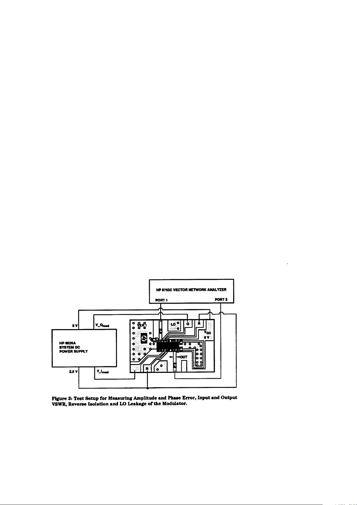
by applying 1.75 V to the I and/or
Q inputs.
Amplitude and phase are measured by setting the network analyzer for an S21 measurement at
the center frequency of choice.
Set the port 1 stimulus level to the
LO level you intend to use in your
circuit (-12 dBm for the data
sheet).
By adjusting the Vi and Vq settings
you can step around the I/Q vector circle, reading magnitude and
phase at each point. The relative
values of phase and gain (amplitude) at the various points will
indicate the accuracy of the
modulator. Note: you must use
very low ripple power supplies for
the reference, V
Imod
, and V
Qmod
supplies. Ripple or noise of only a
few millivolts will appear as wob-
bling phase readings on the network analyzer.
The same test setup shown below
is used to measure input and output VSWR, reverse isolation, and
power vs. frequency. V
Imod
and
V
Qmod
are set to 3.25 V and the
appropriate frequency ranges are
swept. S11 provides input VSWR
data, S22 provides output VSWR
data and S12 provides reverse
isolation data. S21 provides power
output (add the source power to
the S21 derived gain).
LO leakage data shown in figure
17 is generated by setting V
Imod
=
V
Qmod
= V
Iref
= V
Qref
= 2.5 volts then
performing an S21 sweep. Since
phase is not important for these
measurements, a scalar network
analyzer or a signal generator and
spectrum analyzer could be used.
HPMX-2005 Typical Data
Measurement
Direct measurement of the amplitude and phase error at the output
is the most accurate way to evaluate modulator performance. By
measuring the error directly, all
the harmonics, LO leakage, etc.
that show up in the output signal
are accounted for. Figure 3 below
shows the test setup that was
used to create the amplitude and
phase error plots (figures 19 and
21).
Amplitude and phase error are
measured by using the four channel power supply to simulate I and
Q input signals. Real 1.5 V
p-p
I and
Q signals would swing 0.75 volts
above and below an average 2.5 V
level, therefore, a logic “high”
level input is simulated by applying 3.25 V, and a logic “low” level
Page 5

7-58
HPMX-2005 Typical Performance
Figure 4. HPMX-2005 Device Current
vs. Temperature. VCC = 5 V, LO =
-12␣ dBm, V
Iref
= V
Qref
= 2.5 V, V
Imod
=
V
Qmod
= 3.25 V, T
A
= 25° C.
Figure 7. HPMX-2005 Power Output
vs. Frequency and Supply Voltage.
LO␣ = -12 dBm, V
Iref
= V
Qref
= 2.5 V, V
Imod
= V
Qmod
= 3.25 V, T
A
= 25° C.
Figure 10. HPMX-2005 LO VSWR vs.
Frequency. VCC = 5 V, LO = -12 dBm,
V
Iref
= V
Qref
= 2.5 V, T
A
= 25° C.
Figure 9. HPMX-2005 Power Output
vs. LO Drive Level at 100 MHz.
VCC=5␣ V, V
Iref
= V
Qref
= 2.5 V, V
Imod
=
V
Qmod
= 3.25 V, T
A
=25°C.
Figure 12. HPMX-2005 Output VSWR
vs. Frequency and Supply Voltage. LO
= -12 dBm, V
Iref
= V
Qref
= 2.5 V, TA =
25°C.
Figure 6. HPMX-2005 Power Output
vs. Frequency and Temperature. VCC =
5 V, LO = -12 dBm, V
Iref=VQref
= 2.5 V,
V
Imod
= V
Qmod
= 3.25 V.
Figure 11. HPMX-2005 Output
Reflection Coefficient vs. Frequency.
VCC = 5 V, LO = -12 dBm, V
Iref
= V
Qref
=
2.5 V, T
A
= 25° C.
Figure 5. HPMX-2005 Device Current
vs. Voltage. VCC = 5 V, LO = -12 dBm,
V
Iref
= V
Qref
= 2.5 V, V
Imod
= V
Qmod
=
3.25␣ V, T
A
= 25° C.
Figure 8. HPMX-2005 Power Output
vs. I/Q Drive Level at 100 MHz.
VCC= 5␣ V, LO = -12 dBm, V
Iref
= V
Qref
=
2.5 V, V
Imod
= V
Qmod
, T
A
= 25° C.
5
12
-55
TEMPERATURE (°C)
10
14
-35 -15
16
20
18
I
d
(mA)
25 45 65 85
6
5
0
V
CC
(VOLTS)
0
10
24
15
25
20
DEVICE CURRENT (mA)
810
I = Q = 2.5 V
CAUTION:
SEE NOTE ON V
CC
ON PAGE 3 FOR
OPERATION HERE.
150
-8
0
FREQUENCY (MHz)
-9
-7
50 100
-6
-4
-5
OUTPUT POWER (dBm)
200 250
+25°C
+85°C
–25°C
150
-8
0
FREQUENCY (MHz)
-9
-7
50 100
-6
-4
-5
OUTPUT POWER (dBm)
200 250
V
CC
5.5 V
5.0 V
4.5 V
4.02.5
I/Q DRIVE LEVEL (VOLTS DC)
-16
-12
3.0 3.5
-8
0
-4
PEAK OUTPUT POWER (dBm)
4.5
-10
-8
-25
LO DRIVE LEVEL (dBm)
-10
-6
-20 -15
-4
0
-2
OUTPUT POWER (dBm)
-5 0
1500
FREQUENCY (MHz)
1
1.5
50 100
2
3
2.5
INPUT VSWR (n:1)
200 250
1500
FREQUENCY (MHz)
0
0.4
50 100
0.6
1
0.8
MAG (Γ
OUT
)
200 250
0.2
ANG (Γ
OUT
) (DEGREES)
-90
0
90
180
-180
ANG
MAG
1500
FREQUENCY (MHz)
0
50 100
2
6
4
OUTPUT VSWR (n:1)
200 250
6 V
5 V
4 V
Page 6

7-59
Figure 15. HPMX-2005 RMS Modula-
tion Error vs. Frequency and Φ␣ Adjust.
VCC = 5 V, LO = -12 dBm, V
Iref
␣=␣ V
Qref
=
2.5 V, √(V
Imod
- 2.5)2 + (V
Qmod
- 2.5)2 =
0.75 V, T
A
= 25° C.
Figure 17. HPMX-2005 LO Leakage vs.
Frequency and Φ Adjust. V
CC
= 5 V,
LO␣ = -12 dBm, V
Iref
= V
Qref
= V
Imod
=
V
Qmod =
2.5 V, T
A
= 25° C.
Figure 16. HPMX-2005 Output Power
vs. Frequency and Φ Adjust. V
CC
= 5 V,
LO = -12 dBm, V
Iref
= V
Qref
= 2.5 V,
V
Imod
␣= V
Qmod
= 3.25 V, T
A
= 25° C.
HPMX-2005 Typical
Performance Using Phase
Adjust
The HPMX-2005 has an internal
phase shifter that in normal use
(pin 9 open circuited) operates
over a frequency range of 25 to
200 MHz. By applying 5 volts to
pin 9, this frequency range can be
raised to beyond 250 MHz. This
page shows HPMX-2005 modulator performance with pin 9 tied
to VCC = 5 V for higher frequency
operation. Using the Φ adjust has
minimal effect on the VSWRs at
the LO port.
Figure 13. HPMX-2005 RMS Amplitude
Error vs. Frequency and Φ Adjust.
VCC = 5 V, LO = -12 dBm, V
Iref
= V
Qref
=
2.5 V, √(V
Imod
- 2.5)2 + (V
Qmod
- 2.5)2 =
0.75 V, T
A
= 25° C.
Figure 14. HPMX-2005 RMS Phase
Error vs. Frequency and Φ Adjust.
VCC = 5 V, LO = -12 dBm, V
Iref
= V
Qref
=
2.5 V, √(V
Imod
- 2.5)2 + (V
Qmod
- 2.5)2 =
0.75 V, T
A
= 25° C.
Figure 18. Connection of Pin 9 for Operation of the
HPMX-2005 at Frequencies Between 140 MHz and
250 MHz.
0
FREQUENCY (MHz)
0
0.4
100
0.6
1
0.8
AMPLITUDE ERROR (dB)
200 300
0.2
Φ ADJ = NC
Φ ADJ = 5 V
0
FREQUENCY (MHz)
0
100
2
6
4
PHASE ERROR (DEGREES)
200 300
Φ ADJ = NC
Φ ADJ = 5 V
0
FREQUENCY (MHz)
0
6
100
9
15
12
RMS ERROR (%)
200 300
3
Φ ADJ = NC
Φ ADJ = 5 V
150
-8
0
FREQUENCY (MHz)
-10
-6
50 100
-4
0
-2
OUTPUT POWER (dBm)
200 250 300
Φ ADJ = NC
Φ ADJ = 5 V
0
FREQUENCY (MHz)
-60
100
-50
-30
-40
LO LEAKAGE (dBm)
200 300
Φ ADJ = NC
Φ ADJ = 5 V
1000 pF
1000 pF
VCC = +5 V
1000 pF
RF
out
Q
ref
Q
mod
I
mod
LO
+
LO
–
1000 pF
1000 pF
I
ref
116
2
15
314
413
512
611
710
89
Φ ADJ. CONNECTION FOR
140-250 MHz OPERATION
Page 7

7-60
HPMX-2005 Modulation Accuracy (Sample Part)
VCC = 5 V, LO = -12 dBm, V
Iref
= V
Qref
= 2.5 V, √(V
Imod
- 2.5)2 + (V
Qmod
- 2.5)2 = 0.75 V, TA = 25° C
(unless otherwise noted).
Figure 24. HPMX-2005 RMS
Modulation Error at 100 MHz vs.
Temperature.
Figure 23. HPMX-2005 RMS Modulation Error vs. Input Phase at 100 MHz. This
value is calculated from the values of amplitude and phase error.
Figure 20. HPMX-2005 RMS Amplitude
Error at 100 MHz vs. Temperature.
Figure 22. HPMX-2005 RMS Phase
Error at 100 MHz vs. Temperature.
Figure 21. HPMX-2005 Phase Error vs. Input Phase at 100 MHz.
Figure 19. HPMX-2005 RMS Amplitude Error vs. Input Phase at 100 MHz.
180
-0.2
0
INPUT PHASE (DEGREES)
-0.4
0
90
0.2
0.4
AMPLITUDE ERROR (dB)
270 360
-0.6
0.6
5
0.1
-55
TEMPERATURE (°C)
0
0.2
-35 -15
0.3
0.5
0.4
MAG ERROR (dB)
25 45 65 85
180
-2
0
INPUT PHASE (DEGREES)
-4
0
90
2
4
PHASE ERROR (DEGREES)
270 360
-6
6
5
1
-55
TEMPERATURE (°C)
0
2
-35 -15
3
5
4
PHASE ERROR (DEGREES)
25 45 65 85
180
1
0
INPUT PHASE (DEGREES)
0
2
90
3
4
RMS ERROR (%)
270 360
5
5
1
-55
TEMPERATURE (°C)
0
2
-35 -15
3
5
4
RMS ERROR (%)
25 45 65 85
Page 8

7-61
HPMX-2005 Single and
Double Sideband
Performance
Single sideband (SSB) and double
sideband (DSB) tests are sometimes used to evaluate modulator
performance. Typical SSB and
DSB output spectrum graphs for
the HPMX-2005 are shown in figures 25 and 26 below. Figure 27
shows the test equipment setup
used to generate this information.
For accurate measurements of
modulator performance and LO
suppression, the phase shift provided by the I and Q signal generators must be very close to 90
degrees and the amplitude of the
two signals must be matched to
within a few millivolts. The I,Q
signal generator must put out low
distortion signals or the spectrum
analyzer will show high harmonic
levels that reflect the performance
of the signal generator, not the
modulator.
HPMX-2005 Typical Sideband Performance Data
VCC = 5 V, LO = -12 dBm, V
Iref
= V
Qref
= 2.5 V, V
Imod
= V
Iref
+ 0.75 V sin(2πfnt), V
Qmod
= V
Qref
+ 0.75 V cos(2πfnt) for
SSB, V
Imod
= V
Qmod
= V
Qref
+ 0.75 V cos(2πfnt) for DSB, fn = 25 kHz, TA = 25°C
Symbol Parameters and Test Conditions Units SSB DSB
P
LSB
Lower Sideband Power Output dBc -8 -11
LO
leak
LO Suppression dBc 33 30
P
USB
Upper Sideband Power Output dBm -38 -11
IM
3
3rd Order Intermodulation Distortion Level dBc NA 33
Figure 25. Single Sideband Output Spectrum. Figure 26. Double Sideband Output Spectrum.
-40
99.9
-80
99.95
-20
0
100 100.05 100.1
-60
FREQUENCY (MHz)
OUTPUT POWER (dBm)
-40
99.9
-80
99.95
-20
0
100 100.05 100.1
-60
FREQUENCY (MHz)
OUTPUT POWER (dBm)
Page 9

7-62
HPMX-2005 Using Offsets
to Improve LO Leakage
It is possible to improve on the
excellent performance of the
HPMX-2005 for applications that
are particularly sensitive to LO
leakage. The amount and nature
of the improvement are best understood by examining figures 28
and 29, below.
LO leakage results when normal
variations in the wafer fabrication
process cause small shifts in the
values of the modulator IC’s internal components. These random
variations create an effect equivalent to slight DC imbalances at the
input of each (I and Q) mixer. The
DC imbalances at the mixer inputs are multiplied by ± 1 at the
LO frequency and show up at the
output of the IC as LO leakage.
It is possible to externally apply
small DC signals to the I and Q inputs and exactly cancel the internally generated DC offsets. This
will result in sharply decreased
LO leakage at precisely the frequency and temperature where
the offsets were applied (see figure 28).
This improvement is not very
useful if it doesn’t hold up over
frequency and temperature
changes. The lower curve in figure
28 shows how the offset-adjusted
LO leakage varies versus
frequency. Note that it remains
below -60␣ dBm over most of the
frequency range shown. In the
20␣ MHz range centered at
100␣ MHz, the level is closer to
-70␣ dBm.
Figure 29 shows the performance
of the offset adjusted LO leakage
over temperature. Note that the
adjusted curve is at a level near 70 dBm over the entire temperature range.
The net result of using externally applied offsets with the
HPMX-2005 is that an LO
leakage level below -50 dBm
can typically be achieved over
both frequency and
temperature.
The magnitude of the required external offset varies randomly from
part to part and between the I and
Q mixers on any given IC. Offsets
can range from -35 mV to +35 mV.
External offsets may be applied
either by varying the average level
of the I and Q modulating signals,
or by varying the voltages at the
I
ref
and Q
ref
pins of the modulator.
Figure 28. LO Leakage vs. Frequency
Without DC Offsets and LO Leakage
vs. Frequency with DC Offsets
Adjusted for Minimum LO Leakage at
100 MHz. VCC = 5 V, LO = -12 dBm,
V
Iref
␣= V
Qref
= 2.5 V, T
A
= 25° C.
Figure 29. LO Leakage with No DC
Offsets at 100 MHz vs. Temperature
(Upper Curve) and LO Leakage with
DC Offsets Adjusted for Minimum
Leakage at 25°C vs. Temperature
(Lower Curve). VCC=5V,
LO␣ =␣ -12␣ dBm, V
Iref
= V
Qref
= 2.5 V.
150
-80
0
FREQUENCY (MHz)
-60
50 100
-40
0
-20
LO LEAKAGE (dBm)
200
-100
NO OFFSETS
WITH OFFSETS
5
-80
-55
TEMPERATURE (°C)
-60
-35 -15
-40
0
-20
POWER (dBm)
25 45 65 85
PLO (OFFSET)
P
LO
P
OUT
Page 10

7-63
HPMX-2005 Modulation
Spectrum Diagrams
Figure 30, below, shows the test
set-up that was used to generate
the GSM, JDC and NADC modulation spectrum diagrams that appear on the following page. The
major differences between these
tests are summarized in the table
below.
The modulation spectra are created by setting the function generator to the appropriate bit-clock
frequency. The pattern generator
is set to produce a pseudorandom
serial bit stream (n = 20) that is
NRZ coded. The pseudorandom
bit stream which simulates the serial data in a digital phone is fed
to the base-band processor that
splits it into a two bit parallel
System Bit Clock Frequency Baseband Filter Channel (LO) Frequency
GSM 270 kHz 0.3 GMSK (HP-8657B) 900 MHz
JDC 42 kHz α = 0.5 π/4 DQPSK (HP-8657D) 950 MHz
NADC 48.6 kHz α = 0.35 π/4 DQPSK (HP-8657D) 835 MHz
stream (I and Q) and then filters
each according to the requirements of the digital telephone system being simulated. The I and Q
signals from the baseband filter
are then DC offset by 2.5 V using
the op-amp circuit. The output of
the modulator is monitored using
a spectrum analyzer.
Page 11

7-64
HPMX-2005 Cellular Telephone Modulation Spectrum Performance
TA = 25°C (unless otherwise noted)
Figure 37. HPMX-2005 NADC
Modulation Spectrum at -40°C.
Figure 38. HPMX-2005 NADC
Modulation Spectrum at 25°C.
Figure 39. HPMX-2005 NADC
Modulation Spectrum at 85°C.
Figure 31. HPMX-2005 GSM
Modulation Spectrum at -40°C.
Figure 32. HPMX-2005 GSM
Modulation Spectrum at 25°C.
Figure 33. HPMX-2005 GSM
Modulation Spectrum at 85°C.
Figure 34. HPMX-2005 JDC
Modulation Spectrum at -40°C.
Figure 35. HPMX-2005 JDC
Modulation Spectrum at 25°C.
Figure 36. HPMX-2005 JDC
Modulation Spectrum at 85°C.
99
FREQUENCY (MHz)
-110
-60
-10
RF OUTPUT POWER (dBm)
100 101
RES BW = 3 kHz
VBW = 30 Hz
SWP = 60.0 SEC.
99
FREQUENCY (MHz)
-110
-60
-10
RF OUTPUT POWER (dBm)
100 101
RES BW = 3 kHz
VBW = 30 Hz
SWP = 60.0 SEC.
99
FREQUENCY (MHz)
-110
-60
-10
RF OUTPUT POWER (dBm)
100 101
RES BW = 3 kHz
VBW = 30 Hz
SWP = 60.0 SEC.
99.875
FREQUENCY (MHz)
-110
-60
-10
RF OUTPUT POWER (dBm)
100 100.125
RES BW = 3 kHz
VBW = 30 Hz
SWP = 7.50 SEC.
99.850
FREQUENCY (MHz)
-110
-60
-10
RF OUTPUT POWER (dBm)
100 100.150
RES BW = 3 kHz
VBW = 30 Hz
SWP = 7.50 SEC.
99.850
FREQUENCY (MHz)
-110
-60
-10
RF OUTPUT POWER (dBm)
100 100.150
RES BW = 3 kHz
VBW = 30 Hz
SWP = 7.50 SEC.
99.875
FREQUENCY (MHz)
-110
-60
-10
RF OUTPUT POWER (dBm)
100 100.125
RES BW = 3 kHz
VBW = 30 Hz
SWP = 9.00 SEC.
99.875
FREQUENCY (MHz)
-110
-60
-10
RF OUTPUT POWER (dBm)
100 100.125
RES BW = 3 kHz
VBW = 30 Hz
SWP = 9.00 SEC.
99.850
FREQUENCY (MHz)
-110
-60
-10
RF OUTPUT POWER (dBm)
100 100.150
RES BW = 3 kHz
VBW = 30 Hz
SWP = 9.00 SEC.
Page 12

7-65
O
Part Number Ordering Information
Part Number Option No. of Devices Container
HPMX-2005 25 Min. Tube
HPMX-2005 T10 1000 7" Reel
Package Dimensions
SO-16 Package
HPMX-2005 Test Board Layout
Finished board size 1.5" x 1" x 1/32"
Material: 1/32" epoxy/fiberglass, 1 oz. copper, both sides,
fused tin/lead coating, both sides.
Note: white “+” marks indicate drilling locations for plated-through via
holes to the groundplane on the bottom side of the board.
4.60 (0.181)
5.20 (0.205)
1.35 (0.053)
1.75 (0.069)
0.15 (0.007)
0.254 (0.010)
0.64 (0.025)
0.77 (0.030)
8°
0°
0.10 (0.004)
0.20 (0.008)
0.45 (0.018)
0.56 (0.022)
0.35 (0.014)
0.45 (0.018)
1.27
(0.050)
TYP.
9.80 (0.385)
10.00 (0.394)
4.60 (0.181)
5.20 (0.205)
5.80 (0.228)
6.20 (0.244)
3.80 (0.150)
4.00 (0.158)
1611521431341251161079
8
PIN:
NOTE: DIMENSIONS ARE IN MILLIMETERS (INCHES).
OPTIONAL FOR
OPERATION TO 250 MHz
1000 pF
1000 pF
VCC = +5 V
1000 pF
RFout
Q
ref
Q
mod
I
mod
LO
+
LO
–
1000 pF
1000 pF
I
ref
1 16
2
15
314
413
512
611
710
89
 Loading...