Page 1

Four Character Smart
Alphanumeric Displays
Technical Data
H
HPDL-1414
HPDL-2416
Features
• Smart Alphanumeric Display
Built-in RAM, ASCII Decoder
and LED Drive Circuitry
• Wide Operating Temperature
Range
-40°C to +85°C
• Fast Access Time
160 ns
• Excellent ESD Protection
Built-in Input Protection Diodes
• CMOS IC for Low Power
Consumption
• Full TTL Compatibility Over
Operating Temperature
Range
VIL = 0.8 V
VIH = 2.0 V
• Wave Solderable
• Rugged Package
Construction
• End-Stackable
• Wide Viewing Angle
Typical Applications
• Portable Data Entry Devices
• Medical Equipment
• Process Control Equipment
• Test Equipment
• Industrial Instrumentation
• Computer Peripherals
• Telecommunication
Instrumentation
Description
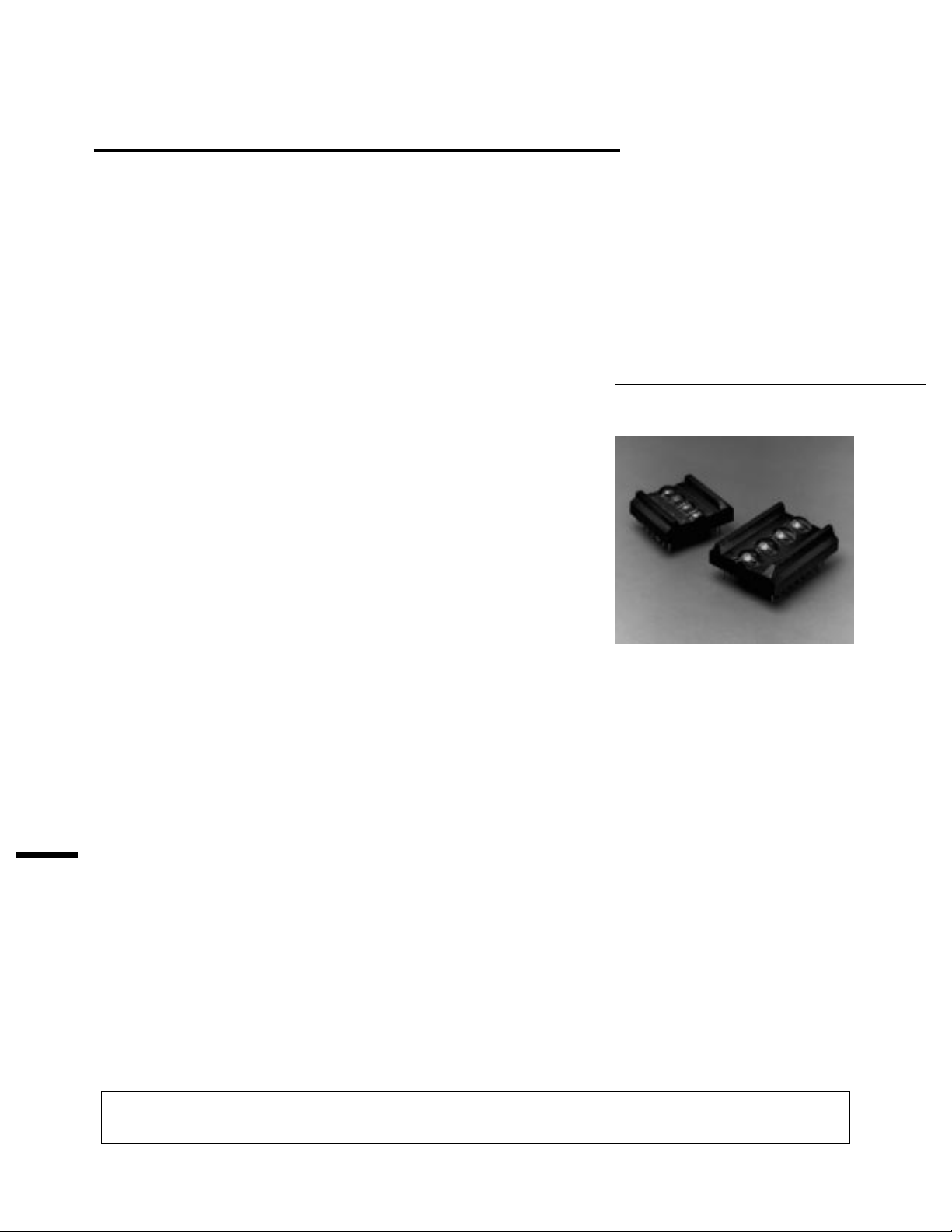
The HPDL-1414 and 2416 are
smart, four character, sixteensegment, red GaAsP displays. The
HPDL-1414 has a character
height of 2.85 mm (0.112"). The
HPDL-2416 has a character
height of 4.10 mm (0.160"). The
on-board CMOS IC contains
memory, ASCII decoder, multiplexing circuitry and drivers. The
monolithic LED characters are
magnified by an immersion lens
which increases both character
size and luminous intensity. The
encapsulated dual-in-line package
provides a rugged, environmentally sealed unit.
The HPDL-1414 and 2416
incorporate many improvements
over competitive products. They
have a wide operating temperature range, very fast IC access
time, and improved ESD protection. The displays are also fully
TTL compatible, wave solderable,
and highly reliable. These
displays are ideally suited for
industrial and commercial
applications where a goodlooking, easy-to-use alphanumeric
display is required.
ESD WARNING: STANDARD CMOS HANDLING PRECAUTIONS SHOULD BE OBSERVED
WITH THE HPDL-1414 AND HPDL-2416.
5964-6381E
3-175
Page 2

Absolute Maximum Ratings
Supply Voltage, VDD to Ground...................................... -0.5 V to 7.0 V
Input Voltage, Any Pin to Ground........................ -0.5 V to VDD + 0.5 V
Free Air Operating Temperature Range, T
[1]
............... -40°C to +85°C
A
Relative Humidity (non-condensing) at 65°C ................................. 90%
Storage Temperature, TS.............................................. -40°C to +85°C
Maximum Solder Temperature, 1.59 mm (0.063 in.)
below Seating Plane, t < 5 sec. ................................................ 260°C
ESD Protection @ 1.5 kΩ, 100 pF ...................... VZ = 2 kV (each Pin)
*All typicals at TA = 25°C.
Package Dimensions
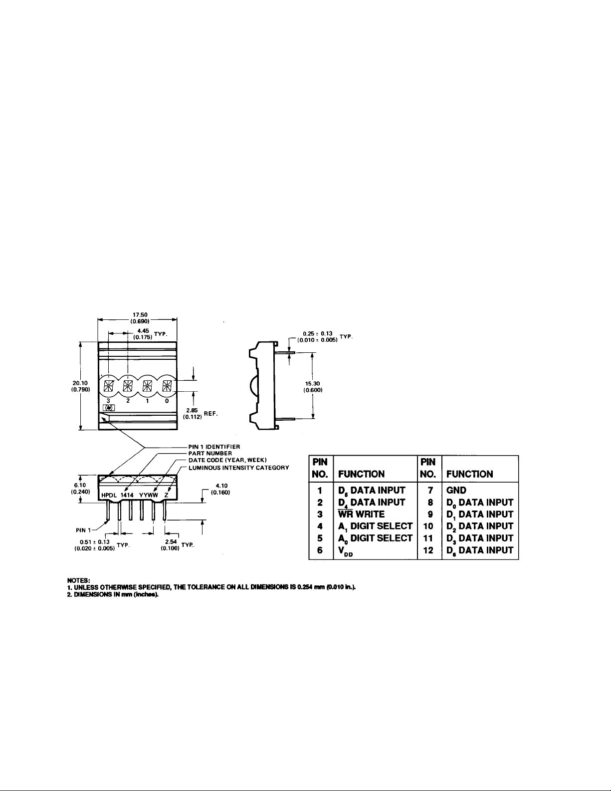
HPDL-1414
3-176
Page 3

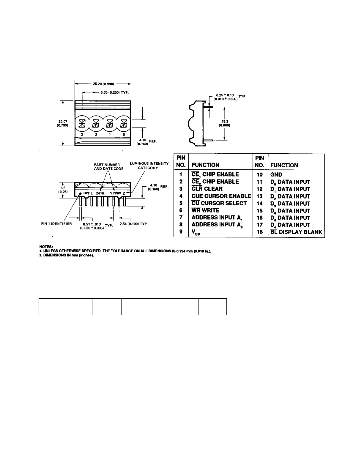
HPDL-2416
Recommended Operating Conditions
Parameter Sym. Min. Nom. Max. Units
Supply Voltage V
DD
4.5 5.0 5.5 V
3-177
Page 4

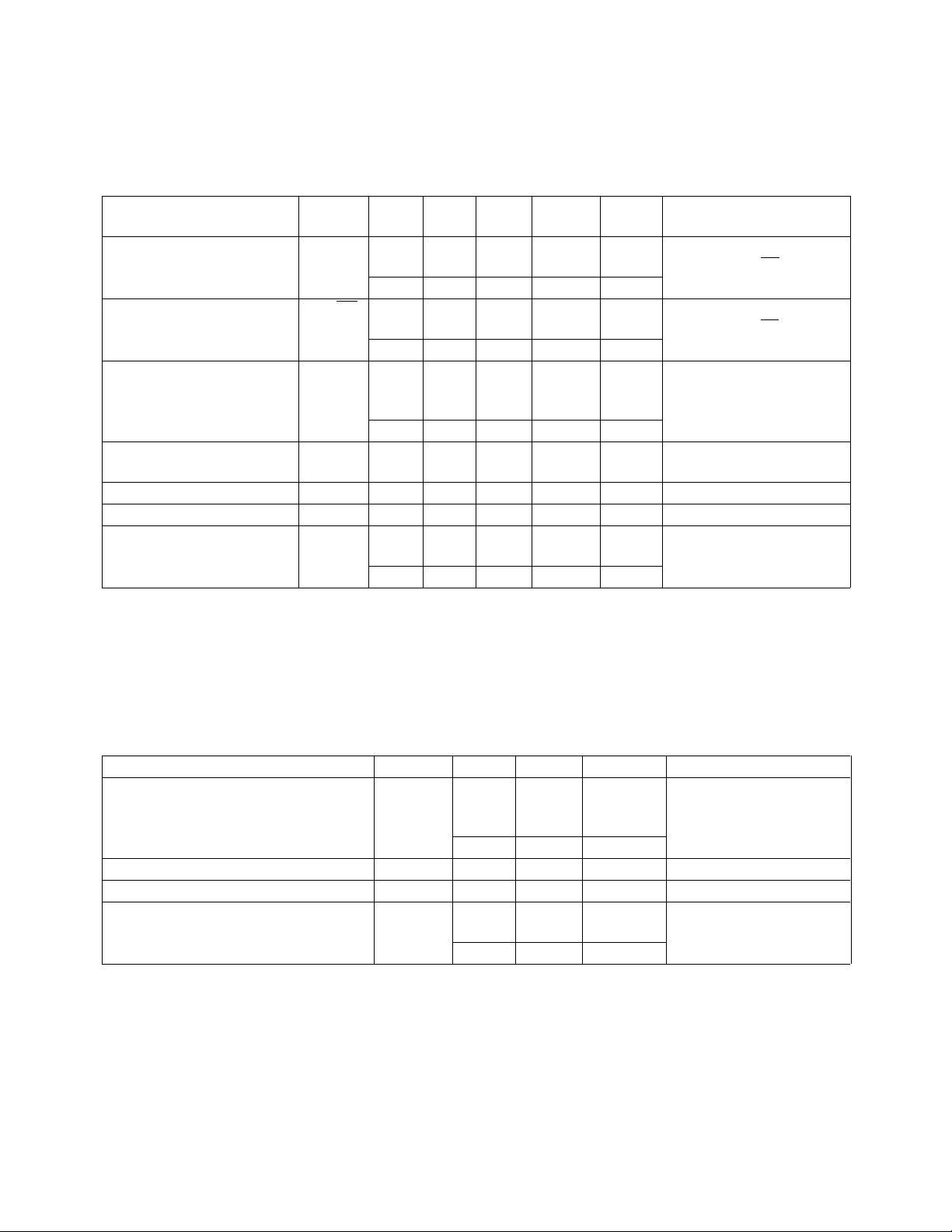
DC Electrical Characteristics over Operating Temperature Range
25°C25°C
Parameter Sym. Min. Typ. Max. Max.
Input Current I
IL
HPDL-1414 17 30 50 µAVDD = 5.0 V, BL = 0.8 V
HPDL-2416 17 30 40 µA
IDD Blank IDD (BL)
HPDL-1414 1.2 2.3 4.0 mA VDD = 5.0 V, BL = 0.8 V
HPDL-2416 1.5 3.5 8.0 mA
IDD 4 Digits ON
(10 Segments/digit)
[2,3]
I
DD
HPDL-1414 70 90 130 mA VDD = 5.0 V
HPDL-2416 85 115 170 mA
IDD 4 Digits ON Cursor
[4]
IDD(CU) 125 165 232 mA VDD = 5.0 V
HPDL-2416
Input Voltage High V
Input Voltage Low V
Power Dissipation
[5]
IH
IL
P
D
2.0 V
GND 0.8 V
HPDL-1414 350 450 715 mW VDD = 5.0 V
HPDL-2416 425 575 910 mW
Notes:
1. VDD = 5.5 V.
2. “%” illuminated in all four characters.
3. Measured at five seconds.
4. Cursor character is sixteen segments and DP ON.
5. Power Dissipation = (VDD)(IDD) for 10 segments ON.
[1]
Units Test Conditions
DD
V
Optical Characteristics at 25°C
[6]
Parameter Sym. Min. Typ. Units Test Conditions
Peak Luminous Intensity per Digit, IV Peak VDD = 5.0 V,
8 segments ON (character average) “*” illuminated in all
HPDL-1414 0.4 1.0 mcd 4 digits
HPDL-2416 0.5 1.25 mcd
Peak Wavelength λ
Dominant Wavelength λ
Peak
d
655 nm
640 nm
Off Axis Viewing Angle
HPDL-1414 ±40 degrees
HPDL-2416 ±50 degrees
3-178
Page 5

AC Timing Characteristics over Operating Temperature Range at VCC = 4.5 V
Parameter Symbol -20°C t
Address Setup Time t
Write Delay Time t
Write Time t
Data Setup Time t
Data Hold Time t
Address Hold Time t
Chip Enable Hold Time
Chip Enable Setup Time
Clear Time
[1]
[1]
[1]
t
CEH
t
CES
t
CLR
AS
WD
W
DS
DH
AH
MIN
90 115 150 ns
10 15 20 ns
80 100 130 ns
40 60 80 ns
40 45 50 ns
40 45 50 ns
40 45 50 ns
90 115 150 ns
2.4 3.5 4.0 ms
Access Time 130 160 200 ns
Refresh Rate 420-790 310-630 270-550 Hz
Note:
1. HPDL-2416 only.
25°C t
MIN
70°C t
MIN
Timing Diagram
Units
3-179
Page 6

Character Set
Magnified Character Font Description
HPDL-1414 HPDL-2416
Relative Luminous Intensity vs. Temperature
3-180
Page 7

Electrical Description
Display Internal Block Diagram HPDL-1414
Figure 1 shows the internal block
diagram of the HPDL-1414. It
consists of two parts: the display
LEDs and the CMOS IC. The
CMOS IC consists of a four-word
ASCII memory, a 64-word character generator, 17 segment drivers,
four digit drivers, and the
scanning circuitry necessary to
multiplex the four monolithic
LED characters. In normal
operation, the divide-by-four
counter sequentially accesses
each of the four RAM locations
and simultaneously enables the
appropriate display digit driver.
The output of the RAM is decoded
by the character generator which,
in turn, enables the appropriate
display segment drivers. Sevenbit ASCII data is stored in RAM.
Since the display uses a 64character decoder, half of the
possible 128 input combinations
are invalid. For each display
location where D5 = D6 in the
ASCII RAM, the display character
is blanked.
Data Entry HPDL-1414
Figure 2 shows a truth table for
the HPDL-1414. Data is loaded
into the display through the
DATA inputs (D6-D0), ADDRESS
inputs (A1-A0), and WRITE (WR).
After a character has been
written to memory, the IC
decodes the ASCII data, drives
the display and refreshes it
without any external hardware or
software.
Figure 1. HPDL-1414 Internal Block Diagram.
3-181
Page 8

Figure 2. HPDL-1414 Write Truth Table.
Display Internal Block Diagram HPDL-2416
Figure 3 shows the internal block
diagram for the HPDL-2416
display. The CMOS IC consists of
a four-word ASCII memory, a
four-word cursor memory, a
64-word character generator, 17
segment drivers, four digit
drivers, and the scanning circuitry
necessary to multiplex the four
monolithic LED characters. In
normal operation, the divide-byfour counter sequentially
accesses each of the four RAM
locations and simultaneously
enables the appropriate display
digit driver. The output of the
RAM is decoded by the character
generator which, in turn, enables
the appropriate display segment
drivers. For each display location,
the cursor enable (CUE) selects
whether the data from the ASCII
RAM (CUE = 0) or the stored
cursor (CUE = 1) is to be
displayed. The cursor character is
denoted by all sixteen segments
and the DP ON. Seven-bit ASCII
data is stored in RAM. Since the
display utilizes a 64-character
decoder, half of the possible 128
input combinations are invalid.
For each display location where
D5 = D6 in the ASCII RAM, the
display character is blanked. The
entire display is blanked when
BL = 0.
Data is loaded into the display
through the data inputs (D6 -D0),
address inputs (A1, A0), chip
enables (CE1, CE2), cursor select
(CU), and write (WR). The cursor
select (CU) determines whether
data is stored in the ASCII RAM
(CU = 1) or cursor memory
(CU = 0). When CE1 = CE2 =
WR = 0 and CU = 1, the information on the data inputs is stored
in the ASCII RAM at the location
specified by the address inputs
(A1, A0). When CE1 = CE2 = WR
= 0 and CU = 0, information on
the data input, D0, is stored in the
cursor at the location specified by
the address inputs (A1, A0). If D
0
= 1, a cursor character is stored
in the cursor memory. If D0 = 0,
a previously stored cursor
character will be removed from
the cursor memory.
If the clear input (CLR) equals
zero for one internal display cycle
(4 ms minimum), the data in the
ASCII RAM will be rewritten with
zeroes and the display will be
blanked. Note that the blanking
input (BL) must be equal to
logical one during this time.
Data Entry HPDL-2416
Figure 4 shows a truth table for
the HPDL-2416 display. Setting
the chip enables (CE1, CE2) to
their low state and the cursor
select (CU) to its high state will
enable data loading. The desired
data inputs (D6-D0) and address
inputs (A1, A0) as well as the chip
enables (CE1, CE2) and cursor
select (CU) must be held stable
during the write cycle to ensure
that the correct data is stored
into the display. Valid ASCII data
codes are shown in Figure 1. The
display accepts standard sevenbit ASCII data. Note that D6 ≠ D
for the codes shown in Figure 4.
If D6 = D5 during the write cycle,
then a blank will be stored in the
display. Data can be loaded into
the display in any order. Note
that when A1 = A0 = 0, data is
stored in the furthest right-hand
display location.
Cursor Entry HPDL-2416
As shown in Figure 4, setting the
chip enables (CE1, CE2) to their
low state and the cursor select
(CU) to its low state will enable
cursor loading. The cursor
character is indicated by the
display symbol having all 16
segments and the DP ON. The
least significant data input (D0),
the address inputs (A1, A0), the
chip enables (CE1, CE2), and the
cursor select (CU) must be held
stable during the write cycle to
5
3-182
Page 9

Figure 3. HPDL-2416 Internal Block Diagram.
3-183
Page 10

ensure that the correct data is
stored in the display. If D0 is in a
low state during the write cycle,
then a cursor character will be
removed at the indicated
location. If D0 is in a high state
during the write cycle, then a
cursor character will be stored at
the indicated location. The
presence or absence of a cursor
character does not affect the
ASCII data stored at that location.
Again, when A1 = A0 = 0, the
cursor character is stored in the
furthest right-hand display
location.
All stored cursor characters are
displayed if the cursor enable
(CUE) is high. Similarly, the
stored ASCII data words are
displayed, regardless of the
cursor characters, if the cursor
enable (CUE) is low. The cursor
enable (CUE) has no effect on the
storage or removal of the cursor
characters within the display. A
flashing cursor is displayed by
pulsing the cursor enable (CUE).
For applications not requiring a
cursor, the cursor enable (CUE)
can be connected to ground and
the cursor select (CU) can be
connected to VCC. This inhibits
the cursor function and allows
only ASCII data to be loaded into
the display.
Display Clear HPDL-2416
As shown in Figure 4, the ASCII
data stored in the display will be
cleared if the clear (CLR) is held
low and the blanking input (BL)
is held high for 4 ms minimum.
The cursor memory is not
affected by the clear (CLR) input.
Cursor characters can be stored
or removed even while the clear
(CLR) is low. Note that the
display will be cleared regardless
of the state of the chip enables
(CE1, CE2). However, to ensure
that all four display characters
are cleared, CLR should be held
low for 4 ms following the last
write cycle.
Function BL CLR CUE CU CE1CE2WR A1A0D6D5D4D3D2D1D0DIG3DIG2DIG1DIG
Write L X X H L L L L L a a aaaaaNCNCNC
Data -OR- L H b b bbbbbNCNC NC
Memory X H X H L L L H L c c cccccNC NCNC
Disable X X X H X X H X X X X XXXXX Previously Written
Data X X X H X H X Data
Memory X X X H H X X
Write
Write X X X L L L L L L X X XXXXHNCNCNC
Cursor L H X X XXXXHNCNC NC
Clear X X X L L L L L L X X XXXXLNCNCNC
Cursor L H X X XXXXLNCNC NC
Disable X X X L X X H X X X X XXXXX Previously Written
Cursor X X X L X H X Cursor
Memory X X X L H X X
L = LOGIC LOW INPUT “a” = ASCII CODE CORRESPODING TO SYMBOL “ ”
H = LOGIC HIGH INPUT NC = NO CHANGE
X = DON’T CARE = CURSOR CHARACTER (ALL SEGMENTS ON)
Figure 4a. Cursor/Data Memory Write Truth Table.
Function BL CLR CUE CU CE1CE2WR DIG3DIG2DIG1DIG
CUE HH LXXXX Display previously written data
HH HXXXX Display previously written cursor
Clear H L XXXXX Clear data memory, cursor memory
*NOTE: CLR should be held low for 4 ms
following the last WRITE cycle to ensure
all data is cleared.
Blanking L X XXXXX Blank display, data and cursor"
Figure 4b. Displayed Data Truth Table.
HHddddddd NCNCNC
HLXXXXXXHNC NCNC
HHXXXXXXH NCNCNC
HLXXXXXXLNC NCNC
HHXXXXXXL NCNCNC
0
*
unchanged
memories unchanged.
0
3-184
Page 11

Display Blank HPDL-2416
As shown in Figure 4, the display
will be blanked if the blanking
input (BL) is held low. Note that
the display will be blanked
regardless of the state of the chip
enables (CE1, CE2) or write (WR)
inputs. The ASCII data stored in
the display and the cursor
memory are not affected by the
blanking input. ASCII data and
cursor data can be stored even
while the blanking input (BL) is
low. Note that while the blanking
input (BL) is low, the clear (CLR)
function is inhibited. A flashing
display can be obtained by
applying a low frequency square
wave to the blanking input (BL).
Because the blanking input (BL)
also resets the internal display
multiplex counter, the frequency
applied to the blanking input
(BL) should be much slower than
the display multiplex rate. Finally,
dimming of the display through
the blanking input (BL) is not
recommended.
For further application information please consult Application
Note 1026.
Optical Considerations/ Contrast Enhancement
The HPDL-1414 and HPDL-2416
displays use a precision aspheric
immersion lens to provide
excellent readability and low offaxis distortion. For the HPDL1414, the aspheric lens produces
a magnified character height of
2.85 mm (0.112 in.) and a
viewing angle of ±40°. For the
HPDL-2416, the aspheric lens
produces a magnified character
height of 4.1 mm (0.160 in.) and
a viewing angle of ±50°. These
features provide excellent
readability at distances up to 1.5
metres (4 feet) for the HPDL-
1414 and 2 metres (6 feet) for
the HPDL-2416.
Each HPDL-1414/2416 display is
tested for luminous intensity and
marked with an intensity category
on the side of the display
package. To ensure intensity
matching for multiple package
applications, mixing intensity
categories for a given panel is not
recommended.
The HPDL-1414/2416 display is
designed to provide maximum
contrast when placed behind an
appropriate contrast enhancement filter. For further information on contrast enhancement,
see Hewlett-Packard Application
Note 1015.
Mechanical and Electrical Considerations
The HPDL-1414/2416 are dual inline packages that can be stacked
horizontally and vertically to
create arrays of any size. These
displays are designed to operate
continuously between -40°C to
+85°C with a maximum of 10
segments on per digit.
During continuous operation of
all four Cursors the operating
temperature should be limited to
-40°C to +55°C. At temperatures
above +55°C, the maximum
number of Cursors illuminated
continuously should be reduced
as follows: No Cursors illuminated at operating temperatures
above 75°C. One Cursor can be
illuminated continuously at
operating temperatures below
75°C. Two Cursors can be
illuminated continuously at
operating temperatures below
68°C. Three Cursors can be
illuminated continuously at
operating temperatures below
60°C.
The HPDL-1414/2416 are assembled by die attaching and wire
bonding the four GaAsP/GaAs
monolithic LED chips and the
CMOS IC to a high temperature
printed circuit board. An
immersion lens is formed by
placing the PC board assembly
into a nylon lens filled with
epoxy. A plastic cap creates an
air gap to protect the CMOS IC.
Backfill epoxy environmentally
seals the display package. This
package construction provides
the display with a high tolerance
to temperature cycling.
The inputs to the CMOS IC are
protected against static discharge
and input current latchup.
However, for best results
standard CMOS handling
precautions should be used. Prior
to use, the HPDL-1414/2416
should be stored in anti-static
tubes or conductive material.
During assembly a grounded
conductive work area should be
used, and assembly personnel
should wear conductive wrist
straps. Lab coats made of
synthetic material should be
avoided since they are prone to
static charge build-up. Input
current latchup is caused when
the CMOS inputs are subjected
either to a voltage below ground
(VIN < ground) or to a voltage
higher than VDD (VIN > VDD) and
when a high current is forced into
the input. To prevent input
current latchup and ESD damage,
unused inputs should be
connected either to ground or to
VDD. Voltages should not be
applied to the inputs until V
has been applied to the display.
Transient input voltages should
be eliminated.
DD
3-185
Page 12

Soldering and Post Solder Cleaning Instructions
The HPDL-1414/2416 may be
hand soldered or wave soldered
with SN63 solder. Hand soldering
may be safely performed only
with an electronically
temperature-controlled and
securely grounded soldering iron.
For best results, the iron tip
temperature should be set at
315°C (600°F). For wave
soldering, a rosin-based RMA flux
can be used. The solder wave
temperature should be
245°C ± 5°C (473°F ± 9°F),
and the dwell in the wave should
be set at 11/2 to 3 seconds for
optimum soldering. Preheat
temperature should not exceed
93°C (200°F) as measured on the
solder side of the PC board.
For further information on
soldering and post solder
cleaning, see Application Note
1027, Soldering LED
Components.
3-186
 Loading...