

Page 1
HN58X2402SI/HN58X2404SI
Two-wire serial interface
2k EEPROM (256-word × 8-bit)
4k EEPROM (512-word × 8-bit)
ADE-203-1105A (Z)
Rev. 1.0
Nov. 30, 2000
Description
HN58X24xxSI series are two-wire serial interface EEPROM (Electrically Erasable and Programmable
ROM). They realize high speed, low power consumption and a high level of reliability by employing
advanced MNOS memory technology and CMOS process and low voltage circuitry technology. They also
have a 8-byte page programming function to make their write operation faster.
Note: Hitachi’s serial EEPROM are authorized for using consumer applications such as cellular phone,
camcorders, audio equipment. Therefore, please contact Hitachi’s sales office before using
industrial applications such as automotive systems, embedded controllers, and meters.
Features
• Single supply: 1.8 V to 5.5 V
• Two-wire serial interface (I2CTM serial bus*1)
• Clock frequency: 400 kHz
• Power dissipation:
Standby: 3 µA (max)
Active (Read): 1 mA (max)
Active (Write): 3 mA (max)
• Automatic page write: 8-byte/page
• Write cycle time: 10 ms (2.7 V to 5.5 V)/15ms (1.8 V to 2.7 V)
• Endurance: 105 Cycles (Page write mode)
• Data retention: 10 Years
Page 2
HN58X2402SI/HN58X2404SI
• Small size packages: TSSOP 8-pin and SOP 8-pin
• Shipping tape and reel
TSSOP 8-pin: 3,000 IC/reel
SOP 8-pin: 2,500 IC/reel
Note: 1. I2C is a trademark of Philips Corporation.
Ordering Information
Type No. Internal organization Operating voltage Frequency Package
HN58X2402SFPI 2k bit (256 × 8-bit) 1.8 V to 5.5 V 400 kHz 150 mil 8-pin plastic SOP
(FP-8DB)
HN58X2404SFPI 4k bit (512 × 8-bit)
HN58X2402STI 2k bit (256 × 8-bit) 1.8 V to 5.5 V 400 kHz 8-pin plastic TSSOP
(TTP-8DA)
HN58X2404STI 4k bit (512 × 8-bit)
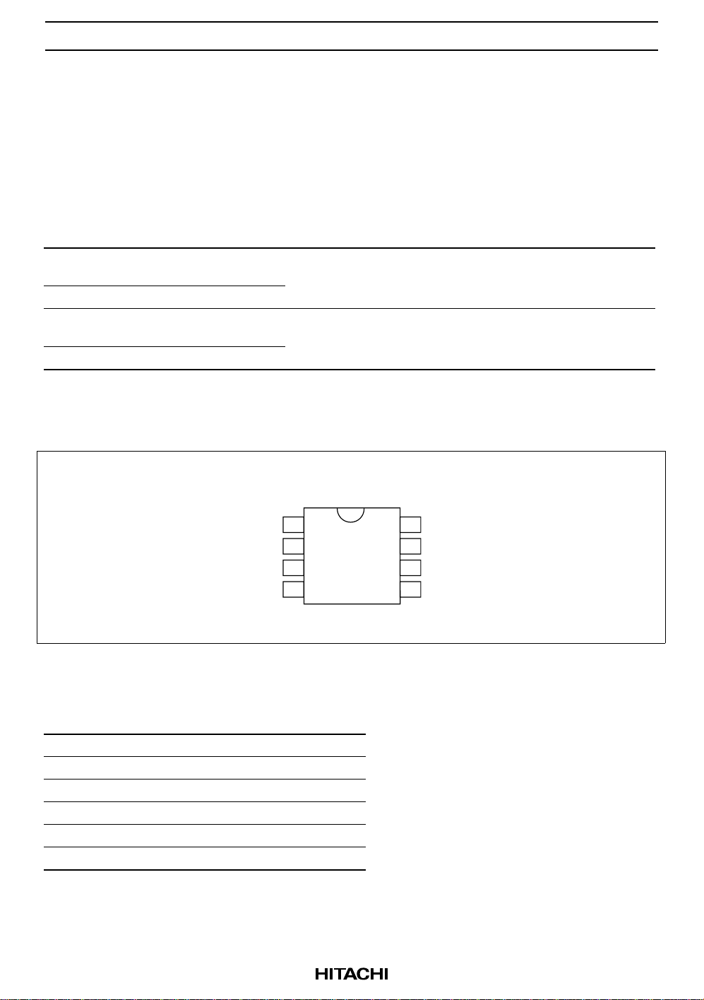
Pin Arrangement
A0
A1
A2
V
SS
Pin Description
Pin name Function
A0 to A2 Device address
SCL Serial clock input
SDA Serial data input/output
WP Write protect
V
CC
V
SS
Power supply
Ground
8-pin TSSOP
8-pin SOP
1
2
3
4
(Top view)
8
7
6
5
V
CC
WP
SCL
SDA
2
Page 3
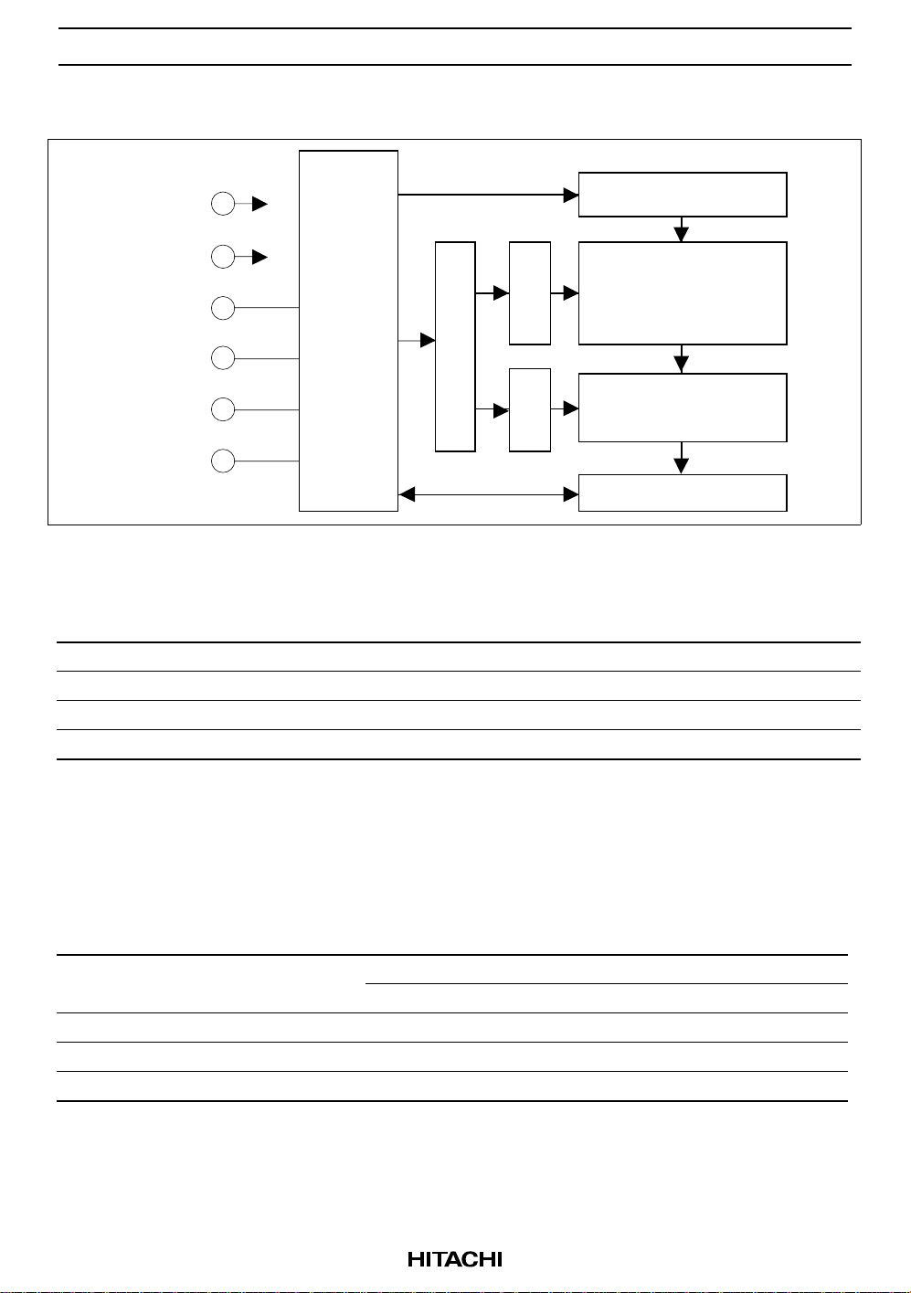
Block Diagram
HN58X2402SI/HN58X2404SI
V
CC
V
SS
High voltage generator
Memory array
WP
Control
logic
X decoderY decoder
A0, A1, A2
SCL
Address generator
Y-serect & Sense amp.
SDA
Serial-parallel converter
Absolute Maximum Ratings
Parameter Symbol Value Unit
Supply voltage relative to V
Input voltage relative to V
SS
SS
Operating temperature range*
1
V
CC
Vin –0.5*2 to +7.0*
Topr –40 to +85 ˚C
Storage temperature range Tstg –65 to +125 ˚C
Notes: 1. Including electrical characteristics and data retention.
2. Vin (min): –3.0 V for pulse width 50 ns.
3. Should not exceed V
+ 1.0 V.
CC
–0.6 to +7.0 V
3
V
DC Operating Conditions
Parameter Symbol Min Typ Max Unit
Supply voltage V
Input high voltage V
Input low voltage V
CC
V
SS
IH
IL
Operating temperature Topr –40 — 85 ˚C
Note: 1. VIL (min): –1.0 V for pulse width 50 ns.
1.8 — 5.5 V
000V
VCC × 0.7 — VCC + 1.0 V
1
–0.3*
—V
× 0.3 V
CC
3
Page 4
HN58X2402SI/HN58X2404SI
DC Characteristics (Ta = –40 to +85˚C, VCC = 1.8 V to 5.5 V)
Parameter Symbol Min Typ Max Unit Test conditions
Input leakage current I
Output leakage current I
Standby VCC current I
Read VCC current I
Write VCC current I
Output low voltage V
LI
LO
SB
CC1
CC2
OL2
V
OL1
Capacitance (Ta = 25˚C, f = 1 MHz)
Parameter Symbol Min Typ Max Unit
Input capacitance (A0 to A2, SCL, WP) Cin*
Output capacitance (SDA) C
Note: 1. This parameter is sampled and not 100% tested.
— — 2.0 µA VCC = 5.5 V, Vin = 0 to 5.5 V (SCL, SDA)
——20µAVCC = 5.5 V, Vin = 0 to 5.5 V (A0 to A2, WP)
— — 2.0 µA VCC = 5.5 V, Vout = 0 to 5.5 V
— 1.0 3.0 µA Vin = VSS or V
CC
— — 1.0 mA VCC = 5.5 V, Read at 400 kHz
— — 3.0 mA VCC = 5.5 V, Write at 400 kHz
— — 0.4 V VCC = 4.5 to 5.5 V, IOL = 1.6 mA
V
= 2.7 to 4.5 V, IOL = 0.8 mA
CC
V
= 1.8 to 2.7 V, IOL = 0.4 mA
CC
— — 0.2 V VCC = 1.8 to 2.7 V, IOL = 0.2 mA
1
— — 6.0 pF Vin = 0 V
1
*
I/O
— — 6.0 pF Vout = 0 V
Test
conditions
4
Page 5

HN58X2402SI/HN58X2404SI
AC Characteristics (Ta = –40 to +85˚C, VCC = 1.8 to 5.5 V)
Test Conditions
• Input pules levels:
VIL = 0.2 × V
VIH = 0.8 × V
• Input rise and fall time: 20 ns
• Input and output timing reference levels: 0.5 × V
• Output load: TTL Gate + 100 pF
Parameter Symbol Min Typ Max Unit Notes
Clock frequency f
Clock pulse width low t
Clock pulse width high t
Noise suppression time t
Access time t
Bus free time for next mode t
Start hold time t
Start setup time t
Data in hold time t
Data in setup time t
Input rise time t
Input fall time t
Stop setup time t
Data out hold time t
Write cycle time VCC = 2.7 V to 5.5 V t
Notes: 1. This parameter is sampled and not 100% tested.
2. t
WC
CC
CC
CC
— — 400 kHz
1200 — — ns
600 — — ns
— — 50 ns 1
100 — 900 ns
1200 — — ns
600 — — ns
600 — — ns
0——ns
100 — — ns
— — 300 ns 1
— — 300 ns 1
600 — — ns
50 — — ns
— — 10 ms 2
— — 15 ms 2
VCC = 1.8 V to 2.7 V t
SCL
LOW
HIGH
I
AA
BUF
HD.STA
SU.STA
HD.DAT
SU.DAT
R
F
SU.STO
DH
WC
WC
is the time from a stop condition to the end of internally controlled write cycle.
5
Page 6
HN58X2402SI/HN58X2404SI
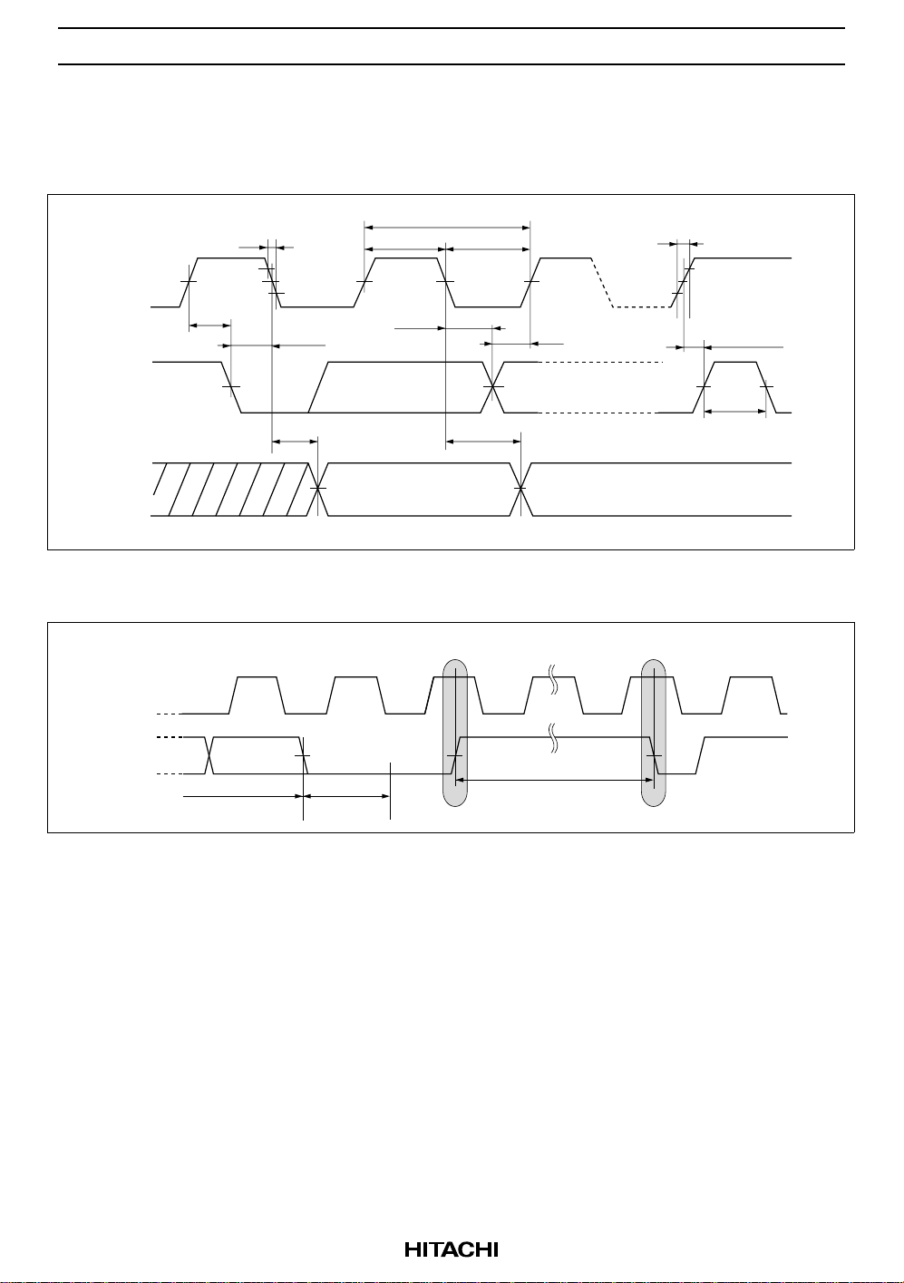
Timing Waveforms
Bus Timing
t
F
SCL
t
SU.STA
t
HD.STA
t
HIGH
t
HD.DAT
1/f
SCL
t
LOW
t
SU.DAT
t
R
t
SU.STO
SDA
(in)
SDA
(out)
Write Cycle Timing
SCL
SDA
(Address (n))
t
AA
D0 in
Write data ACK
t
DH
Stop condition Start condition
t
WC
(Internally controlled)
t
BUF
6
Page 7

HN58X2402SI/HN58X2404SI
Pin Function
Serial Clock (SCL)
The SCL pin is used to control serial input/output data timing. The SCL input is used to positive edge
clock data into EEPROM device and negative edge clock data out of each device. Maximum clock rate is
400 kHz.
Serial Input/Output data (SDA)
The SDA pin is bidirectional for serial data transfer. The SDA pin needs to be pulled up by resistor as that
pin is open-drain driven structure. Use proper resistor value for your system by considering VOL, IOL and
the SDA pin capacitance. Except for a start condition and a stop condition which will be discussed later,
the SDA transition needs to be completed during SCL low period.
Data Validity (SDA data change timing waveform)
SCL
SDA
Data
change
Note: High-to-low and low-to-high change of SDA should be done during SCL low periods.
Data
change
7
Page 8

HN58X2402SI/HN58X2404SI
Device Address (A0, A1, A2)
UP to eight devices for 2k, four devices for 4k, can be addressed on the same bus by setting the levels on
these pins to different combinations. The levels on these pins are compared with the device address code
which are input through the SDA pin. The device is selected if the compare is successfully done. These
pins are internally pulled-down to VSS. The device read these pins as Low if unconnected. As for 4k, it is
unneccesary for the A0 pin to be connected because the corresponding device address code is used as
memory address a8.
Pin Connections for A0 to A2
Pin connection
Max connect
Memory size
2k bit 8 VCC/VSS*1VCC/VSSVCC/V
4k bit 4 VCC/VSSVCC/VSS×*
Notes: 1. “VCC/VSS” means that the device address pins are connected to VCC or VSS. These pins are VSS if
number A2 A1 A0 Notes
unconnected.
2. × = Don’t care (Open is also approval.)
SS
2
Use A0 for memory address a8
Write Protect (WP)
When the Write Protect pin (WP) is high, the write protections feature is enabled and operates as shown in
the following table. When the WP is low, write operations for all memory array are allowed. The read
operation is always activated irrespective of the WP pin status. The WP pin is internally pull-down to VSS.
Write operations for all memory array are allowed if unconnected.
Write Protect Area
Write protect area
WP pin status 2k bit 4k bit
V
IH
V
IL
Entire (2k bit) Entire (4k bit)
Normal read/write operation
8
Page 9

HN58X2402SI/HN58X2404SI
Functional Description
Start Condition
A high-to-low transition of the SDA with the SCL high is needed in order to start read, write operation.
(See start condition and stop condition)
Stop Condition
A low-to-high transition of the SDA with the SCL high is a stop condition. The stand-by operation starts
after a read sequence by a stop condition. In the case of write operation, a stop condition terminates the
write data inputs and place the device in a internally-timed write cycle to the memories. After the
internally-timed write cycle which is specified as tWC, the device enters a standby mode. (See write cycle
timing)
Start Condition and Stop Condition
SCL
SDA
(in)
Stop conditionStart condition
9
Page 10

HN58X2402SI/HN58X2404SI
Acknowledge
All addresses and data words are serially transmitted to and from in 8-bit words. The receiver sends a zero
to acknowledge that it has received each word. This happens during ninth clock cycle. The transmitter
keeps bus open to receive acknowledgment from the receiver at the ninth clock. In the write operation,
EEPROM sends a zero to acknowledge after receiving every 8-bit words. In the read operation, EEPROM
sends a zero to acknowledge after receiving the device address word. After sending read data, the
EEPROM waits acknowledgment by keeping bus open. If the EEPROM receives zero as an acknowledge,
it sends read data of next address. If the EEPROM receives acknowledgment "1" (no acknowledgment) and
a following stop condition, it stops the read operation and enters a stand-by mode. If the EEPROM
receives neither acknowledgment "0" nor a stop condition, the EEPROM keeps bus open without sending
read data.
Acknowledge Timing Waveform
SCL
SDA IN
SDA OUT
12 89
Acknowledge
out
10
Page 11

HN58X2402SI/HN58X2404SI
Device Addressing
The EEPROM device requires an 8-bit device address word following a start condition to enable the chip
for a read or a write operation. The device address word consists of 4-bit device code, 3-bit device address
code and 1-bit read/write(R/W) code. The most significant 4-bit of the device address word are used to
distinguish device type and this EEPROM uses “1010” fixed code. The device address word is followed by
the 3-bit device address code in the order of A2, A1, A0. The device address code selects one device out of
all devices which are connected to the bus. This means that the device is selected if the inputted 3-bit
device address code is equal to the corresponding hard-wired A2-A0 pin status. As for the 4kbit
EEPROMs, some bits of their device address code may be used as the memory address bits. For example,
A0 is used as a8 of memory address for the 4kbit. The eighth bit of the device address word is the
read/write(R/W) bit. A write operation is initiated if this bit is low and a read operation is initiated if this bit
is high. Upon a compare of the device address word, the EEPROM enters the read or write operation after
outputting the zero as an acknowledge. The EEPROM turns to a stand-by state if the device code is not
“1010” or device address code doesn’t coincide with status of the correspond hard-wired device address
pins A0 to A2.
Device Address Word
Device address word (8-bit)
Device code (fixed) Device address code*
2k 1010A2 A1 A0 R/W
4k 1010A2 A1 a8 R/W
Notes: 1. A2 to A0 are device address and a8 are memory address.
2. R/W=“1” is read and R/W = “0” is write.
1
R/W code*
2
11
Page 12

HN58X2402SI/HN58X2404SI
Write Operations
Byte Write:
A write operation requires an 8-bit device address word with R/W = “0”. Then the EEPROM sends
acknowledgment "0" at the ninth clock cycle. After these, EEPROMs receive 8-bit memory address word.
Upon receipt of this memory address, the EEPROM outputs acknowledgment "0" and receives a following
8-bit write data. After receipt of write data, the EEPROM outputs acknowledgment "0". If the EEPROM
receives a stop condition, the EEPROM enters an internally-timed write cycle and terminates receipt of
SCL, SDA inputs until completion of the write cycle. The EEPROM returns to a standby mode after
completion of the write cycle.
Byte Write Operation
2k, 4k
Device
address
1010 W
Start
Memory
address (n) Write data (n)
a7a6a5a4a3a2a1a0D7D6D5D4D3D2D1
ACK ACK ACK
R/W
D0
Stop
Page Write:
The EEPROM is capable of the page write operation which allows any number of bytes up to 8 bytes to be
written in a single write cycle. The page write is the same sequence as the byte write except for inputting
the more write data. The page write is initiated by a start condition, device address word, memory
address(n) and write data(Dn) with every ninth bit acknowledgment. The EEPROM enters the page write
operation if the EEPROM receives more write data(Dn+1) instead of receiving a stop condition. The a0 to
a2 address bits are automatically incremented upon receiving write data(Dn+1). The EEPROM can
continue to receive write data up to 8 bytes. If the a0 to a2 address bits reaches the last address of the page,
the a0 to a2 address bits will roll over to the first address of the same page and previous write data will be
overwritten. Upon receiving a stop condition, the EEPROM stops receiving write data and enters
internally-timed write cycle.
Page Write Operation
2k, 4k
Start
Device
address
1010
Memory
address (n) Write data (n+m)Write data (n)
W
a7a6a5a4a3a2a1
ACK
R/W
a0
D7D6D5D4D3D2D1
ACK ACK
D0
D5D4D3D2D1
D0
Stop
ACK
12
Page 13

HN58X2402SI/HN58X2404SI
Acknowledge Polling:
Acknowledge polling feature is used to show if the EEPROM is in a internally-timed write cycle or not.
This features is initiated by the stop condition after inputting write data. This requires the 8-bit device
address word following the start condition during a internally-timed write cycle. Acknowledge polling will
operate R/W code = “0”. Acknowledgment “1” (no acknowledgment) shows the EEPROM is in a
internally-timed write cycle and acknowledgment “0” shows that the internally-timed write cycle has
completed. See Write Cycle Polling using ACK.
Write Cycle Polling using ACK
Send
write command
Send
stop condition
to initiate write cycle
Send
start condition
Proceed write operation
Send
device address word
with R/W = 0
ACK
returned
Yes
Next operation is
addressing the memory
Yes
Send
memory address
Proceed random address
read operation
No
No
Send
start condition
Send
stop condition
Send
stop condition
13
Page 14

HN58X2402SI/HN58X2404SI
Read Operation
There are three read operations: current address read, random read, and sequential read. Read operations are
initiated the same way as write operations with the exception of R/W = “1”.
Current Address Read:
The internal address counter maintains the last address accessed during the last read or write operation,
with incremented by one. Current address read accesses the address kept by the internal address counter.
After receiving a start condition and the device address word(R/W is “1”), the EEPROM outputs the 8-bit
current address data from the most significant bit following acknowledgment “0” If the EEPROM receives
acknowledgment “1” (no acknowledgment) and a following stop condition, the EEPROM stops the read
operation and is turned to a standby state. In case the EEPROM have accessed the last address of the last
page at previous read operation, the current address will roll over and returns to zero address. In case the
EEPROM have accessed the last address of the page at previous write operation, the current address will
roll over within page addressing and returns to the first address in the same page. The current address is
valid while power is on. The current address after power on will be indefinite. The random read operation
described below is necessary to define the memory address.
Current Address Read Operation
Device
address Read data (n+1)
2k, 4k
Start
Note: 1. Don‘t care bit for 4k.
1010 R
1
*
D7D6D5D4D3D2D1
ACK No ACK
R/W
D0
Stop
14
Page 15

HN58X2402SI/HN58X2404SI
Random Read:
This is a read operation with defined read address. A random read requires a dummy write to set read
address. The EEPROM receives a start condition, device address word(R/W=0) and memory address
sequentially. The EEPROM outputs acknowledgment “0” after receiving memory address then enters a
current address read with receiving a start condition. The EEPROM outputs the read data of the address
which was defined in the dummy write operation. After receiving acknowledgment “1”(no
acknowledgment) and a following stop condition, the EEPROM stops the random read operation and
returns to a standby state.
Random Read Operation
2k, 4k
Start
Device
address
@@@ # # #
1010 1010
Memory
address (n) Read data (n)
WR
a7a6a5a4a3a2a1
ACK
R/W
Dummy write Currect address read
a0
Device
address
Start
ACK
D6D7D4D3D2D1D0
ACK
R/W
D5
No ACK
Stop
Note: 1. 2nd device address code (#) should be same as 1st (@).
Sequential Read:
Sequential reads are initiated by either a current address read or a random read. If the EEPROM receives
acknowledgment “0” after 8-bit read data, the read address is incremented and the next 8-bit read data are
coming out. This operation can be continued as long as the EEPROM receives acknowledgment “0”. The
address will roll over and returns address zero if it reaches the last address of the last page. The sequential
read can be continued after roll over. The sequential read is terminated if the EEPROM receives
acknowledgment “1” (no acknowledgment) and a following stop condition.
Sequential Read Operation
Device
address Read data (n+m)Read data (n) Read data (n+1) Read data (n+2)
2k, 4k
1010
Start
R
D7D6D5D4D3D2D1D0D7D6D5D4D3D2D1D0D7D6D5D4D3D2D1
ACK
ACK ACK No ACK
R/W
ACK
D0
D5D4D3D2D1
Stop
D0
15
Page 16

HN58X2402SI/HN58X2404SI
Notes
Data protection at VCC On/Off
When VCC is turned on or off, noise on the SCL and SDA inputs generated by external circuits (CPU, etc)
may act as a trigger and turn the EEPROM to unintentional program mode. To prevent this unintentional
programming, this EEPROM have a power on reset function. Be careful of the notices described below in
order for the power on reset function to operate correctly.
• SCL and SDA should be fixed to VCC or VSS during VCC on/off. Low to high or high to low transition
during VCC on/off may cause the trigger for the unintentional programming.
• VCC should be turned off after the EEPROM is placed in a standby state.
• VCC should be turned on from the ground level(VSS) in order for the EEPROM not to enter the
unintentional programming mode.
• VCC turn on speed should be longer than 10 us.
Write/Erase Endurance and Data retention Time
The endurance is 105 cycles in case of page programming and 104 cycles in case of byte programming (1%
cumulative failure rate). The data retention time is more than 10 years when a device is page-programmed
less than 104 cycles.
Noise Suppression Time
This EEPROM have a noise suppression function at SCL and SDA inputs, that cut noise of width less than
50 ns. Be careful not to allow noise of width more than 50 ns.
16
Page 17

Package Dimensions
HN58X2402SFPI/HN58X2404SFPI (FP-8DB)
4.89
5.15 Max
8
5
HN58X2402SI/HN58X2404SI
Unit: mm
14
0.69 Max
1.27
+0.063
*0.42
–0.064
0.40 ± 0.06
*Dimension including the plating thickness
Base material dimension
3.90
+ 0.114
– 0.038
0.14
0.25
1.73 Max
0.10
M
6.02 ± 0.18
+ 0.034
– 0.017
0.20 ± 0.03
*0.22
0.60
Hitachi Code
JEDEC
EIAJ
Weight
1.06
+ 0.289
– 0.194
(reference value)
0° – 8°
FP-8DB
—
—
0.08 g
17
Page 18

HN58X2402SI/HN58X2404SI
HN58X2402STI/HN58X2404STI (TTP-8DA)
3.00
3.30 Max
85
4.40
14
0.65
+0.08
*0.22
–0.07
0.20 ± 0.06
0.805 Max
0.13
M
Unit: mm
1.00
6.40 ± 0.20
0.10
1.10 Max
*Dimension including the plating thickness
Base material dimension
0.15 ± 0.04
*0.17 ± 0.05
+0.03
–0.04
0.07
0° – 8°
Hitachi Code
JEDEC
EIAJ
Mass
(reference value)
0.50 ± 0.10
TTP-8DA
—
—
0.034 g
18
Page 19

HN58X2402SI/HN58X2404SI
Cautions
1. Hitachi neither warrants nor grants licenses of any rights of Hitachi’s or any third party’s patent,
copyright, trademark, or other intellectual property rights for information contained in this document.
Hitachi bears no responsibility for problems that may arise with third party’s rights, including
intellectual property rights, in connection with use of the information contained in this document.
2. Products and product specifications may be subject to change without notice. Confirm that you have
received the latest product standards or specifications before final design, purchase or use.
3. Hitachi makes every attempt to ensure that its products are of high quality and reliability. However,
contact Hitachi’s sales office before using the product in an application that demands especially high
quality and reliability or where its failure or malfunction may directly threaten human life or cause risk
of bodily injury, such as aerospace, aeronautics, nuclear power, combustion control, transportation,
traffic, safety equipment or medical equipment for life support.
4. Design your application so that the product is used within the ranges guaranteed by Hitachi particularly
for maximum rating, operating supply voltage range, heat radiation characteristics, installation
conditions and other characteristics. Hitachi bears no responsibility for failure or damage when used
beyond the guaranteed ranges. Even within the guaranteed ranges, consider normally foreseeable
failure rates or failure modes in semiconductor devices and employ systemic measures such as failsafes, so that the equipment incorporating Hitachi product does not cause bodily injury, fire or other
consequential damage due to operation of the Hitachi product.
5. This product is not designed to be radiation resistant.
6. No one is permitted to reproduce or duplicate, in any form, the whole or part of this document without
written approval from Hitachi.
7. Contact Hitachi’s sales office for any questions regarding this document or Hitachi semiconductor
products.
Hitachi, Ltd.
Semiconductor & Integrated Circuits.
Nippon Bldg., 2-6-2, Ohte-machi, Chiyoda-ku, Tokyo 100-0004, Japan
Tel: Tokyo (03) 3270-2111 Fax: (03) 3270-5109
URL NorthAmerica : http://semiconductor.hitachi.com/
Europe : http://www.hitachi-eu.com/hel/ecg
Asia : http://sicapac.hitachi-asia.com
Japan : http://www.hitachi.co.jp/Sicd/indx.htm
For further information write to:
Hitachi Semiconductor
(America) Inc.
179 East Tasman Drive,
San Jose,CA 95134
Tel: <1> (408) 433-1990
Fax: <1>(408) 433-0223
Hitachi Europe GmbH
Electronic Components Group
Dornacher Straße 3
D-85622 Feldkirchen, Munich
Germany
Tel: <49> (89) 9 9180-0
Fax: <49> (89) 9 29 30 00
Hitachi Europe Ltd.
Electronic Components Group.
Whitebrook Park
Lower Cookham Road
Maidenhead
Berkshire SL6 8YA, United Kingdom
Tel: <44> (1628) 585000
Fax: <44> (1628) 585160
Hitachi Asia Ltd.
Hitachi Tower
16 Collyer Quay #20-00,
Singapore 049318
Tel : <65>-538-6533/538-8577
Fax : <65>-538-6933/538-3877
URL : http://www.hitachi.com.sg
Hitachi Asia Ltd.
(Taipei Branch Office)
4/F, No. 167, Tun Hwa North Road,
Hung-Kuo Building,
Taipei (105), Taiwan
Tel : <886>-(2)-2718-3666
Fax : <886>-(2)-2718-8180
Telex : 23222 HAS-TP
URL : http://www.hitachi.com.tw
Copyright © Hitachi, Ltd., 2000. All rights reserved. Printed in Japan.
Hitachi Asia (Hong Kong) Ltd.
Group III (Electronic Components)
7/F., North Tower,
World Finance Centre,
Harbour City, Canton Road
Tsim Sha Tsui, Kowloon,
Hong Kong
Tel : <852>-(2)-735-9218
Fax : <852>-(2)-730-0281
URL : http://www.hitachi.com.hk
Colophon 2.0
19
 Loading...