

Page 1
HMU16, HMU17
Data Sheet November 1999
16 x 16-Bit CMOS Parallel Multipliers
The HMU16 and HMU17 are high speed, low power CMOS
16-bit x 16-bit multipliers ideal forfast,realtimedigitalsignal
processing applications.
The X and Y operands along with their mode controls (TCX
and TCY) have 17-bit input registers. The mode controls
independently specify the operands as either two’s
complement orunsignedmagnitude format, thereby allowing
mixed mode multiplication operations.
Two16-bit output registers are provided to hold the most and
least significant halves of the result (MSP and LSP). For
asynchronous output, these registers may be made
transparent through the use of the Feedthrough Control
(FT).
Additional inputs are provided for format adjustment and
rounding. The Format Adjust control (FA) allows the user to
select either a left shifted 31-bit product or a full 32-bit
product, whereas the round control (RND) provides the
capability of rounding the most significant portion of the
result.
The HMU16 has independent clocks (CLKX, CLKY, CLKL,
CLKM) associated with each of these registers to maximize
throughput and simplify bus interfacing. The HMU17 has
only a single clock input (CLK), but makes use of three
register enables (
inputs control the X and Y Input Registers, while
controls both the MSP and LSP Output Registers. This
configuration facilitates the use of the HMU17 for
microprogrammed systems.
The two halves of the product may be routed to a single
16-bit three-state output port via a multiplexer, and in
addition, the LSP is connected to the Y-input port through a
separate three-state buffer.
ENX, ENY and ENP). The ENX and ENY
ENP
File Number 2803.4
Features
• 16 x 16-Bit Parallel Multiplier with Full 32-Bit Product
• High-Speed (35ns) Clocked Multiply Time
• Low Power Operation
-I
-I
• Supports Two’s Complement, Unsigned Magnitude and
Mixed Mode Multiplication
• HMU16 is Compatible with the AM29516, LMU16,
IDT7216 and the CY7C516
• HMU17 is Compatible with the AM29517, LMU17,
IDT7217 and the CY7C517
• TTL Compatible Inputs/Outputs
• Three-State Outputs
= 500µA Maximum
CCSB
= 7.0mA Maximum at 1MHz
CCOP
Applications
• Fast Fourier Transform Analysis
• Digital Filtering
• Graphic Display Systems
• Image Processing
• Radar and Sonar
• Speech Synthesis and Recognition
Ordering Information
TEMP.
PART NUMBER
HMU16JC-35 0 to 70 68 Ld PLCC N68.95
HMU16JC-45 0 to 70 68 Ld PLCC N68.95
HMU16GC-35 0 to 70 68 Ld CPGA G68.B
HMU16GC-45 0 to 70 68 Ld CPGA G68.B
HMU17JC-35 0 to 70 68 Ld PLCC N68.95
HMU17JC-45 0 to 70 68 Ld PLCC N68.95
HMU17GC-35 0 to 70 68 Ld CPGA G68.B
HMU17GC-45 0 to 70 68 Ld CPGA G68.B
RANGE (oC) PACKAGE
PKG.
NO.
1
CAUTION: These devices are sensitive to electrostatic discharge; follow proper IC Handling Procedures.
1-888-INTERSIL or 407-727-9207
| Copyright © Intersil Corporation 1999
Page 2
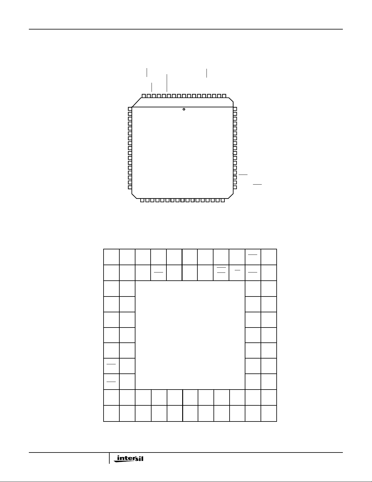
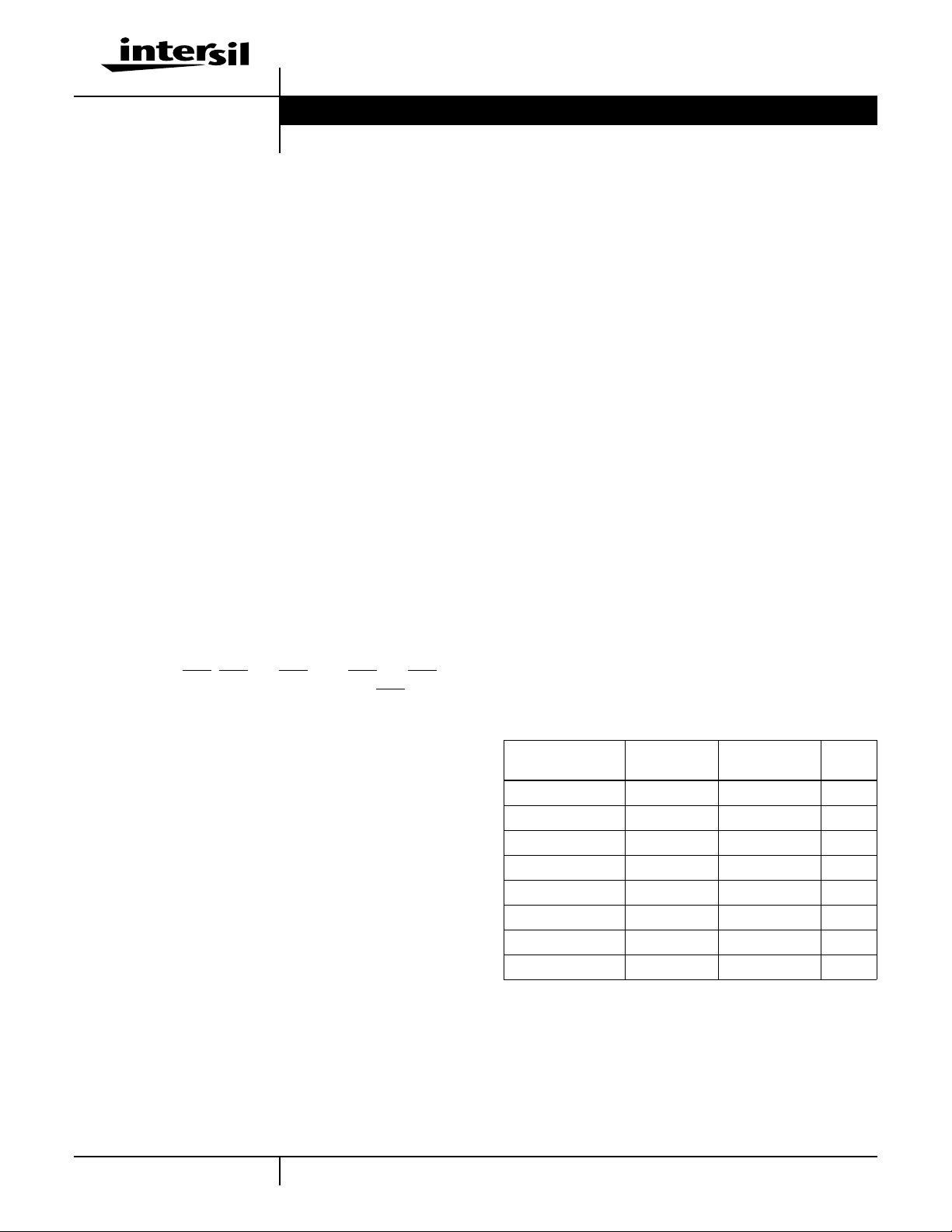
Pinouts
P15, P31
P14, P30
P13, P29
P12, P28
P11, P27
P10, P26
P9, P25
P8, P24
P7, P23
P6, P22
P5, P21
P4, P20
P3, P19
P2, P18
P1, P17
P0, P16
NC
OEP
CLKM (ENP)
NC
10
11
12
13
14
15
16
17
18
19
20
21
22
23
24
25
26
27282930313233
HMU16, HMU17
68 LEAD PLCC
TOP VIEW
FAFTMSPSEL
GND
GND
VCCVCCTCY
TCX
RND
123456789
6867666564636261
ENX)
CLKX (
X15
X14
43424140393837363534
X13
60
59
58
57
56
55
54
53
52
51
50
49
48
47
46
45
44
NC
X12
X11
X10
X9
X8
X7
X6
X5
X4
X3
X2
X1
X0
OEL
CLKL (CLK)
CLKY (
ENY)
11
10
9
8
7
6
5
4
3
N/C
X11
X12
X9
X10
X7
X8
X5
X6
X3
X4
X1
X2
X0
OEL
CLKL
CLKY
(
ENY) (CLK)
Y15, P15
X13
X14
Y14, P14
Y13, P13
Y12, P12
X15
CLKX
(ENX)
Y9, P9
Y8, P8
Y7, P7
Y11, P11
Y10, P10
Y6, P6
68 LEAD CPGA
TOP VIEW
TCY
RND
V
TCX
CC
Y5, P5
Y4, P4
GND
Y3, P3
V
CC
Y2, P2
Y1, P1
GND
MSP
Y0, P0
SEL
NC
FT
FA
OEP
CLKM
ENP)
(
P30/
P14 P15
P28/
P12 P13
P26/
P10 P11
P24/
P8 P9
P22/
P6 P7
P20/
P4
P18/
P2
N/C
P31/
P29/
P27/
P25/
P23/
P21/
P5
P19/
P3
Y10/
Y12/
Y13/
Y14/
Y15/
N/C
Y0/P0
Y2/P2
Y1/P1
Y3/P3
BA KLCD E F GH J
2
1
Y4/P4
Y5/P5
Y6/P6
Y7/P7
Y8/P8
Y9/P9
P10 P12 P14
Y11/
P11 P13 P15
P16/
N/C
P17/
P1P0
2
Page 3
Functional Block Diagrams
HMU16, HMU17
HMU16
CLKX
CLKY
FA
FT
CLKM
CLKL
MSPSEL
OEP
X0 - 15 TCX
REGISTER
RND TCY Y0 - 15/PO - 15
REGISTER REGISTER
OEL
MULTIPLIER ARRAY
FORMAT ADJUST
MSP
RESISTER
MULTIPLEXER
P16 - 31/PO - 15
LSP
RESISTER
CLK
ENX
ENY
FA
FT
ENP
MSPSEL
OEP
HMU17
X0 - 15
TCX TCX RND TCY Y0 - 15/PO - 15
REGISTERREGISTER
MULTIPLIER ARRAY
FORMAT ADJUST
MSP
RESISTER
REGISTER
RESISTER
MULTIPLEXER
OEL
LSP
P16 - 31/PO - 15
3
Page 4
HMU16, HMU17
Pin Description
PLCC PIN
SYMBOL
V
CC
GND 2, 3 GND. The device ground.
X0-X15 47-59, 61-63 I X-Input Data. These 16 data inputs provide the multiplicand which may be in two's complement
Y0-Y15/
P0-P15
P16-P31/
P0-P15
TCY, TCX 66, 67 I Two's Complement Control. Input data is interpreted as two's complement when this control is
FT 5 I Feed through Control. When this control is HIGH, both the MSP and LSP Registers are
FA 6 I FormatAdjust Control. A full 32-bit product is selected when this control line is HIGH. A LOW on
RND 65 I Round Control. When this control is HIGH, a one is added to the Most Significant Bit (MSB) of the
MSPSEL 4 I Output Multiplexer Control. When this control is LOW, the MSP is available for output at the
OEL 46 I Y-In/P0-15Output Port Three-State Control. When OELis HIGH, the output drivers are inthe high
OEP 7 I P16-31/P0-15 Output Port Three-State Control. A LOW on this control line enables the output
THE FOLLOWING PIN DESCRIPTIONS APPLY TO THE HMU16 ONLY
CLKX 64 I X-Register Clock. The rising edge of this clock loads the X-data Input Register along with the TCX
CLKY 44 I Y-Register Clock. The rising edge of this clock loads the Y-data Input Register along with the TCY
CLKM 8 I MSPRegister Clock. The rising edge of CLKM loads the Most Significant Product (MSP) Register.
CLKL 45 I LSP Register Clock. The rising edge of CLKL loads the Least Significant Product (LSP) Register.
THE FOLLOWING PIN DESCRIPTIONS APPLY TO THE HMU17 ONLY
CLK 45 I Clock. The rising edge of this clock will load all enabled registers.
ENX 64 I X-Register Enable. When ENX is LOW, the X-register is enabled; X-input data and TCX will be
ENY 44 I Y-Register Enable. ENY enables the Y-register. (See ENX).
ENP 8 I Product Register Enable. ENP enables the Product Register. Both the MSP and LSP
NUMBER TYPE DESCRIPTION
1, 68 VCC. The +5V power supply pins. A 0.1µF capacitor between the VCC and GND pins is
recommended.
or unsigned magnitude format.
27-42 I/O Y-Input/LSP Output Data. This 16-bit port is used to provide the multiplier which may be in two's
complement or unsigned magnitude format. It may also be used for output of the Least Significant
Product (LSP).
10-25 O Output Data. This 16-bit port may provide either the MSP (P16-31) or the LSP (P0-15).
HIGH. A LOW indicates the data is to be interpreted as unsigned magnitude format.
transparent. When LOW, the registers are latched by their associated clock signals.
this control line selects a left shifted 31-bit product with the sign bit replicated in the LSP. This
control is normally HIGH, except for certain two's complement integer and fractional
applications.
LSP. This position is dependent on the FAcontrol; FA = HIGH indicates RND adds to the 2-15 bit
(P15), and FA = LOW indicates RND adds to the 2
dedicated output port, and the LSP is available at the Y-input/LSP output port. When MSPSEL is
HIGH, the LSP is available at both ports and the MSP is not available for output.
impedance state. This state is required for Ydata input. When OEL is LOW, the port is enabled for
LSP output.
port. When OEP is HIGH, the output drivers are in the high impedance state.
and RND Registers.
and RND Registers.
latched at the rising edge of CLK. When ENX is high, the X-register is in a hold mode.
Sections are enabled by ENP. (See ENX).
-16
bit (P14).
4
Page 5

HMU16, HMU17
Functional Description
The HMU16/HMU17 are high speed 16 x 16-bit multipliers
designed to perform very fast multiplication of two 16-bit
binary numbers. The two 16-bit operands (X and Y) may be
independently specified as either two's complement or
unsigned magnitude format by the two's complement
controls (TCX and TCY). When either of these control lines
is LOW, the respective operand is treated as an unsigned
16-bit value; and when it is HIGH, the operand is treated as
a signed value represented in two's complement format. The
operands along with their respective controls are latched at
the rising edge of the associated clock signal. The HMU16
accomplishes this through the use of independent clock
inputs for each of the Input Registers (CLKX and CLKY),
while the HMU17 utilizes a single clock signal (CLK) along
with the X and Y register enable inputs (
Input controls are also provided for rounding and format
adjustment of the 32-bit product. The Round input (RND) is
provided to accommodate rounding of the most significant
portion of the product by adding one to the Most Significant
Bit (MSB) of the LSP Register. The position of the MSB is
dependent on the state of the Format Adjust Control (see
Pin Descriptions and Multiplier Input/Output Format Tables).
The Round input is latched into the RND Register whenever
either of the input registers is clocked. The Format Adjust
control (
the
when
the sign bit replicated in bit position 15 of the LSP. The
control must be HIGH for unsigned magnitude, and mixed
mode multiplication operations. It may be LOW for certain
two'scomplement integer and fractional operations only (see
Multiplier Input/ Output Formats Table).
FA) allows the product output to be formatted. When
FA control is HIGH, a full 32-bit product is output; and
FA is LOW, a left-shifted 31-bit product is output with
ENX and ENY).
FA
The HMU16/HMU17 multipliers are equipped with two 16-bit
Output Registers (MSP and LSP) which are provided to hold
the most and least significant portions of the resultant
product respectively. The HMU16 uses independent clocks
(CLKM and CLKL) for latching the two output registers, while
the HMU17 uses a single clock input (CLK) along with the
Product Latch Enable (
may also be made transparent for asynchronous output
through the use of the Feed through Control (FT). There are
two output configurations which may be selected when using
the HMU16/HMU17 multipliers. The first configuration allows
the simultaneous access of the most and least significant
halves of the product. When the
Most Significant Product will be available at the dedicated
output port (P16-31/P0-15). The Least Significant Product is
simultaneously available at the bidirectional port shared with
the Y-inputs (Y0-15/P0-15) through the use of the LSP
output enable (
multiplexing the MSP and LSP Registers onto the dedicated
output port through the use of the
the
MSPSEL control is LOW, the Most Significant Product
will be available at the dedicated output port; and when
MSPSEL is HIGH, the Least Significant Product will be
availableat this port. This configuration allows access of the
entire 32-bit product by a 16-bit wide system bus.
OEL). The other output configuration involves
ENP). The MSP and LSP Registers
MSPSEL input is LOW, the
MSPSEL control. When
5
Page 6
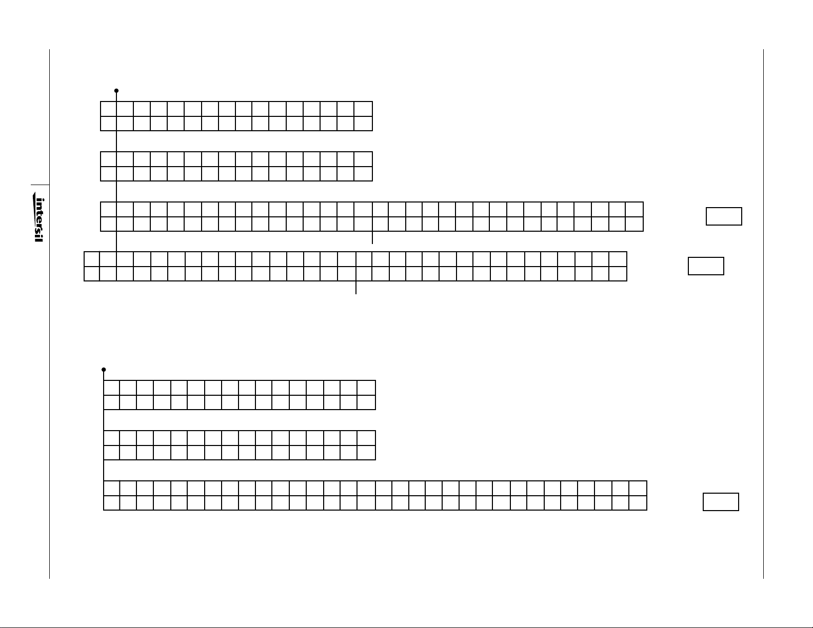
Multiplier Input/Output Formats
BINARY POINT
X
X
X
14
15
-1-20
2
2
X
13
12
-3
-2
2
X11X10X9X
-4
-6
2
2-52
8
-7
2
X6X
X
7
-8
2
2
X
5
-11
-10
-9
2
2
X
X
4
-12
2
X
2
3
1
-14
-13
2
2
X
0
-15
2
SIGNAL
DIGIT VALUE
Y
Y
Y
14
15
6
X
* =
-1
-0
2
2
-2
P31P30P29P28P27P26P25P24P23P22P21P20P19P18P17P
-1-20
2
2
Y
13
12
-3
-2
2
-3
-2
2
Y11Y10Y9Y
-4
-4
-6
2
2-52
-6
2
2-52
Y6Y
Y
8
7
-8
-7
2
2
2
-9
-8
-7
2
2
2
Y
5
-11
-10
-9
2
2
-11
-10
2
2
Y
Y
4
-12
2
-12
2
Y
2
3
1
-14
-13
2
2
-14
-13
2
2
MSP
P31P30P29P28P27P26P25P24P23P22P21P20P19P18P17P
=
0-21
-2
2
2-12
-4
-3
2
2-52
-7
-6
2
2
-9
-8
2
2
-11
-10
2
2
2
-12
16
-14
-13
2
2
MSP
SIGNAL
Y
0
-15
DIGIT VALUE
2
P15P14P13P12P11P
16
-15
2
-16
0
2
-2
-18
-17
2
2
P15P14P13P12P11P
-19
-18
-17
-16
-15
2
2
2
2
2
P9P8P7P6P5P4P3P2P1P
10
-26
-25
-24
-23
-22
-21
-20
-19
2
2
2
2
2
2
2
2
LSP
P9P8P7P6P5P4P3P2P1P
10
-27
-26
-25
-24
-23
-22
-21
-20
2
2
2
2
2
2
2
2
LSP
SIGNAL
0
-30
-29
-28
-27
2
2
2
-30
-29
-28
2
2
2
2
SIGNAL
0
DIGIT VALUE
DIGIT VALUE
FIGURE 1. FRACTIONAL TWO’S COMPLEMENT NOTATION
NOTE: In this format an overflow occurs in the attempted multiplication of the two's complement number 1,000 . . . 0 with 1,000 . . . 0 yielding an erroneous product of -1 in the fraction case
and -230 in the integer case.
BINARY POINT
X
X
X
14
15
-2
-1
2
2
2
Y
Y
Y
14
15
X
-2
-1
2
2
2
X
13
12
-4
-3
2
Y
13
12
-4
-3
2
X11X10X9X
-6
-5
2
2-72
Y11Y10Y9Y
-6
-5
2
2-72
X6X
X
8
7
-10
-9
-8
2
2
2
Y6Y
Y
8
7
-10
-9
-8
2
2
2
X
5
-12
-11
2
2
Y
5
-12
-11
2
2
X
X
4
-13
2
Y
4
-13
2
X
2
3
3
1
-15
-14
2
2
Y
Y
2
1
-15
-14
2
2
X
0
-16
2
Y
0
-16
2
SIGNAL
DIGIT VALUE
SIGNAL
DIGIT VALUE
FA = 1
FA = 0
HMU16, HMU17
P31P30P29P28P27P26P25P24P23P22P21P20P19P18P17P
=
-2
-1
2
2
-4
-3
2
2
-6
-5
2
-8
2
2-72
-10
-9
2
2
-12
-11
2
2
-14
-13
2
2
MSP
FIGURE 2. FRACTIONAL UNSIGNED MAGNITUDE NOTATION
P15P14P13P12P11P
16
-16
-15
2
-17
2
2
-19
-18
2
2
-21
-20
2
2
P9P8P7P6P5P4P3P2P1P
10
-29
-28
-27
-26
-25
-24
-23
-22
2
2
2
2
2
2
2
2
-31
-30
2
2
LSP
0
-32
2
SIGNAL
DIGIT VALUE
FA = 1
MANDATORY
Page 7
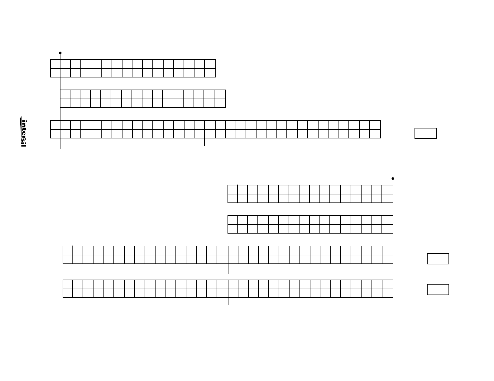
Multiplier Input/Output Formats (Continued)
BINARY POINT
X
X
X
14
15
-1-20
2
Y
Y
15
7
X
-1
2
2
P31P30P29P28P27P26P25P24P23P22P21P20P19P18P17P
=
0
2
2-1-2
X
13
-2
2-32
Y
13
14
-3
-2
-2
2
X11X10X9X
12
-5
-4
2
2
Y11Y10Y9Y
Y
12
-5
2
2-42
-5
-4
-3
2
2
X6X
X
8
7
-9
-6
-6
-6
2
-8
2
2
2-72
Y
8
7
-9
-8
2
2
2-72
-9
-8
-7
2
2
2
5
-10
2
Y6Y
-10
2
-10
2
X
-11
2
-11
2
-11
2
X
X
4
-12
2
Y
5
-12
2
-12
2
X
2
3
4
1
-14
-13
2
2
Y
Y
2
3
-14
-13
2
2
-14
-13
2
2
MSP
FIGURE 3. FRACTIONAL MIXED MODE NOTATION
SIGNAL (TWO’S COMPLEMENT)
X
0
-15
DIGIT VALUE
2
SIGNAL (UNSIGNED MAGNITUDE)
Y
Y
0
1
-16
-15
2
16
-15
2
DIGIT VALUE
2
P15P14P13P12P11P
-19
-18
-17
-16
2
2
2
2
P9P8P7P6P5P4P3P2P1P
10
-30
-29
-28
-27
-26
-25
-24
-23
-22
-21
-20
2
2
2
2
2
2
2
2
2
2
2
LSP
0
-31
2
SIGNAL
DIGIT VALUE
FA = 1
MANDATORY
HMU16, HMU17
BINARY POINT
X
X
X
14
15
14
15
-2
Y
X
-2
2132
Y
Y
14
15
14
15
2132
X
13
12
12
2
Y
13
12
12
2
X11X10X9X
10
11
2
2
Y11Y10Y9Y
10
11
2
2
X6X
X
8
7
7
829
2
2
Y6Y
Y
8
7
7
829
2
2
X
5
2
Y
5
526
2-42
X
X
4
42526
2
Y
4
2
X
2
3
3
3
3
1
122
2
Y
Y
2
1
122
2
X
0
0
2
Y
0
0
2
SIGNAL
DIGIT VALUE
SIGNAL
DIGIT VALUE
P31P30P29P28P27P26P25P24P23P22P21P20P19P18P17P
=
29
30
-2
27
2
2282
25
26
2
2
23
24
2
2
21
22
2
2202
18
19
2
MSP
P
P31P30P29P28P27P26P25P24P23P22P21P20P19P18P17P
P
31P30P29P28P27P26P25P24P23P22P21P20P19P18P17P16
31P30P29P28P27P26P25P24P23P22P21P20P19P18P17P16
19
30
31
30
31
30
31
-2
-2
-2
28
28
28
2
2292
2
2292
2
2292
26
27
26
27
2
2
2
2
2
2
24
25
24
25
2
2
2
2
2
2
22
23
22
23
2
2
2
22
23
24
25
26
27
20
19
20
19
20
2
2212
2
2212
2
2212
P15P14P13P12P11P
16
15
2
2162172
14
30
-2
11
2
2122132
P9P8P7P6P5P4P3P2P1P
10
3
7
10
2
829
2
2
42526
2
2
122
2
LSP
P9P8P7P6P5P4P3P2P1P
P9P8P7P6P5P4P3P2P1P
P15P14P13P12P11P
P15P14P13P12P11P
P15P14P13P12P11P
16
16
16
16
2
2172182
2
2172182
2
2172182
14
15
14
14
2
11
11
11
2
2122132
2
2122132
2
2122132
P9P8P7P6P5P4P3P2P1P
10
10
10
3
7
10
10
10
2
2
2
829
7
829
7
829
2
2
2
2
2
2
42526
3
42526
3
42526
2
2
2
2
2
2
122
122
122
2
2
2
SIGNAL
0
0
DIGIT VALUE
2
SIGNAL
0
0
0
0
0
0
DIGIT VALUE
2
2
2
FA = 0
FA = 1
LSPMSP
FIGURE 4. INTEGER TWO’S COMPLEMENT NOTATION
NOTE: In this format an overflow occurs in the attempted multiplication of the two's complement number 1,000 . . . 0 with 1,000 . . . 0 yielding an erroneous product of -1 in the fraction case
and -230 in the integer case.
Page 8
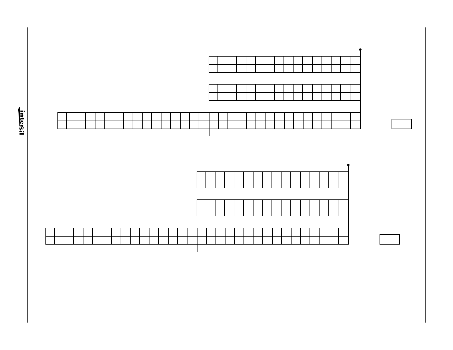
Multiplier Input/Output Formats (Continued)
BINARY POINT
X
X
X
14
15
15
2
2142
X
13
12
12
13
2
X11X10X9X
10
11
2
2
X6X
X
8
7
7
829
2
2
X
5
2
X
X
4
42526
2
X
2
3
3
1
122
2
X
0
0
2
SIGNAL
DIGIT VALUE
Y
Y
Y
14
15
8
P31P30P29P28P27P26P25P24P23P22P21P20P19P18P17P
=
30
31
2
28
2
2292
26
27
2
2
24
25
2
2
22
23
2
20
2212
X
15
2
2142
P15P14P13P12P11P
16
16
2
2172182192
14
15
2
MSP
Y
13
12
12
13
2
2122132
Y11Y10Y9Y
10
11
2
2
P9P8P7P6P5P4P3P2P1P
10
10
11
2
2
Y6Y
Y
8
7
7
829
2
2
7
829
2
2
Y
5
2
2
Y
Y
4
42526
2
42526
2
Y
2
3
3
3
1
122
2
122
2
LSP
FIGURE 5. INTEGER UNSIGNED MAGNITUDE NOTATION
Y
0
0
2
0
0
2
SIGNAL
DIGIT VALUE
SIGNAL
DIGIT VALUE
FA = 1
MANDATORY
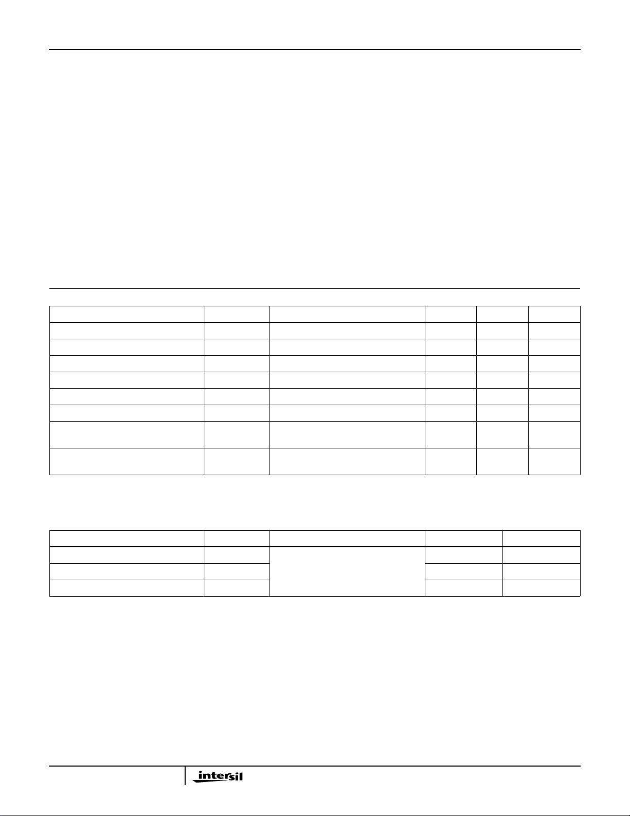
HMU16, HMU17
BINARY POINT
X
P
31P30P29P28P27P26P25P24P23P22P21P20P19P18P17P16
=
31
-2
29
30
2
27
2
2282
25
26
2
2242
22
23
2
2
20
21
2
2
18
19
2
2
MSP
X
X
14
15
14
15
2
2
-2
Y
Y
Y
14
15
X
14
15
2
2
2
P15P14P13P12P11P
16
17
2
2
14
15
2
2
X
13
12
12
13
2
Y
13
12
12
13
2
13
2122
X11X10X9X
11
2102
Y11Y10Y9Y
11
2102
P9P8P7P6P5P4P3P2P1P
10
9
10
11
2
2
X6X
X
8
7
72829
2
Y6Y
Y
8
7
72829
2
7
2
282
X
5
6
2
252
Y
5
6
2
252
6
2
252
LSP
X
X
4
4
Y
4
4
4
X
2
3
3
1
12223
2
Y
Y
2
1
12223
2
1
223
2
2
SIGNAL (TWO’S COMPLEMENT)
X
0
0
DIGIT VALUE
2
SIGNAL (UNSIGNED MAGNITUDE)
Y
0
0
DIGIT VALUE
2
SIGNAL
0
0
DIGIT VALUE
2
FA = 1
MANDATORY
FIGURE 6. INTEGER MIXED MODE NOTATION
Page 9
HMU16, HMU17
Absolute Maximum Ratings Thermal Information
Supply Voltage. . . . . . . . . . . . . . . . . . . . . . . . . . . . . . . . . . . . . +8.0V
Input, Output or I/O Voltage Applied . . . . . GND 0.5V to VCC+0.5V
Storage Temperature Range . . . . . . . . . . . . . . . . . . . 65oC to 150oC
Operating Conditions
Voltage Range. . . . . . . . . . . . . . . . . . . . . . . . . . . .+4.75V to +5.25V
Temperature Range . . . . . . . . . . . . . . . . . . . . . . . . . . . . 0oC to 70oC
CAUTION: Stresses above those listed in the ``Absolute Maximum Ratings'' may cause permanent damage to the device. This is a stress only rating, and operation at
these or any other conditions above those indicated in the operations sections of this specification is not implied.
NOTE:
1. θJA is measured with the component mounted on an evaluation PC board in free air.
Thermal Resistance (Typical, Note 1) θJA(oC/W) θJC (oC/W)
PLCC . . . . . . . . . . . . . . . . . . . . . . . . . . 43.2 15.1
CPGA. . . . . . . . . . . . . . . . . . . . . . . . . . 42.69 10.0
Maximum Package Power Dissipation at 70oC
PLCC . . . . . . . . . . . . . . . . . . . . . . . . . . . . . . . . . . . . . . . . . . .1.7W
CPGA. . . . . . . . . . . . . . . . . . . . . . . . . . . . . . . . . . . . . . . . . . . 2.46
Maximum Junction Temperature
PLCC . . . . . . . . . . . . . . . . . . . . . . . . . . . . . . . . . . . . . . . . . .150oC
CPGA. . . . . . . . . . . . . . . . . . . . . . . . . . . . . . . . . . . . . . . . . .175oC
Maximum Lead Temperature (Soldering, 10s). . . . . . . . . . . . .300oC
Die Characteristics
Gate Count . . . . . . . . . . . . . . . . . . . . . . . . . . . . . . . . . . .4500 Gates
DC Electrical Specifications V
PARAMETER SYMBOL TEST CONDITIONS MIN MAX UNITS
Logical One Input Voltage V
Logical Zero Input Voltage V
Output High Voltage V
Output Low Voltage V
Input Leakage Current I
Output or I/O Leakage Current I
Standby Power Supply Current I
Operating Power Supply Current I
NOTE:
2. Operating Supply Current is proportional to frequency, Typical rating is 5mA/MHz.
Capacitance T
Input Capacitance C
Output Capacitance C
I/O Capacitance C
NOTE:
3. Not tested, but characterized at initial design and at major process/design changes.
= 25oC, Note 3
A
PARAMETER SYMBOL TEST CONDITIONS TYPICAL UNITS
= 5.0V ±5%, TA = 0oC to 70oC
CC
IH
IL
OH
OL
I
O
CCSB
CCOP
IN
OUT
I/O
VCC = 5.25V 2.0 - V
VCC = 4.75V - 0.8 V
IOH = 400mA, VCC = 4.75V 2.6 - V
IOL = +4.0mA, VCC = 4.75V - 0.4 V
VI = VCC or GND, VCC = 5.25V 10 10 µA
VO = VCC or GND, VCC = 5.25V 10 10 µA
VI = VCC or GND, VCC = 5.25V
Outputs Open
VI = VCC or GND, VCC = 5.25V
f = 1MHz (Note 2)
Frequency = 1MHz. All measurements
referenced to device ground.
- 500 µA
- 7.0 mA
15 pF
10 pF
10 pF
9
Page 10
HMU16, HMU17
AC Electrical Specifications V
PARAMETER SYMBOL
Unclocked Multiply Time t
Clocked Multiply Time t
X, Y, RND Setup Time t
X, Y, RND Hold Time t
Clock Pulse Width High t
Clock Pulse Width Low t
MSPSEL to Product Out t
Output Clock to P t
Output Clock to Y t
Three-State Enable Time t
Three-State Disable Time t
Clock Enable Setup Time
= 5.0V ±5%, TA = 0oC to 70oC, Note 6
CC
TEST
CONDITIONS
MUC
MC
S
H
PWH
PWL
PDSEL
PDP
PDY
ENA
DIS
t
SE
Note 4 - 22 - 25 ns
HMU16/HMU17-35 HMU16/HMU17-45
UNITSMIN MAX MIN MAX
- 55 - 70 ns
- 35 - 45 ns
15 - 18 - ns
2-2-ns
10 - 15 - ns
10 - 15 - ns
- 22 - 25 ns
- 22 - 25 ns
- 22 - 25 ns
- 22 - 25 ns
15 - 15 - ns
(HMU17 Only)
Clock Enable Hold Time
t
HE
2-2-ns
(HMU17 Only)
Clock Low Hold Time CLKXY
t
HCL
Note 5 0 - 0 - ns
Relative to CLKML
(HMU16 Only)
Output Rise Time t
Output Fall Time t
From 0.8V to 2.0V - 8 - 8 ns
r
From 2.0V to 0.8V - 8 - 8 ns
f
NOTES:
4. Transition is measured at ±200mV from steady state voltage with loading specified in AC Test Circuit, V1 = 1.5V, R1 = 500Ω
and C1 = 40pF.
5. To ensure the correct product is entered in the output registers, new data may not be entered into the input registers before the output registers
have been clocked.
6. Refer to AC Test Circuit, with V1 = 2.4V, R1 = 500Ω and C1 = 40pF.
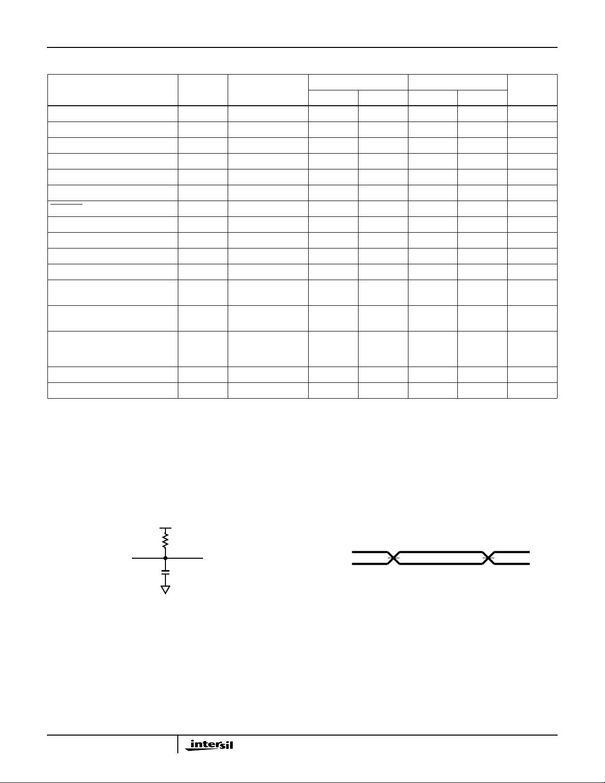
AC Test Circuit
V
1
R
1
DUT
(SEE NOTE)
C
1
NOTE: Includes Stray and Jig Capacitance.
10
AC Testing Input, Output Waveforms
0.3V
0V
1.5V 1.5V
NOTE: AC Testing: All parameters tested as per test circuit. Input
rise and fall times are driven at 1ns/V.
V
OH
V
OL
Page 11
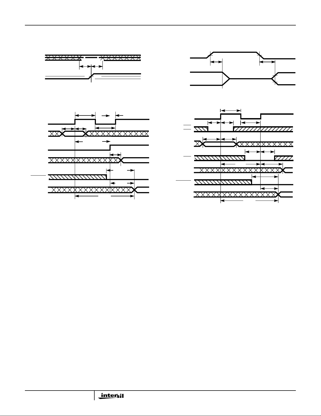
Timing Diagrams
DAT A
INPUT
t
StH
HMU16, HMU17
THREE
3.0V
1.5V
0V
STATE
CONTROL
t
DIS
t
1.5V
ENA
CLOCK
INPUT
CLKX
CLKY
INPUT
XI YI
RND
CLKM
CLKL
OUTPUT Y
MSPSEL
OUTPUT P
3.0V
1.5V
0V
OUTPUT
THREE
STATE
HIGH IMPEDANCE
FIGURE 7. SETUP AND HOLD TIME FIGURE 8. THREE-STATE CONTROL
t
t
PWH
t
HCL
PWH
CLK
t
t
PDP
PWL
t
t
S
H
t
MC
t
PWL
ENX
ENY
INPUT
XI YI
RND
t
t
MUC
t
PDSEL
t
PDP
PDY
ENP
OUTPUT Y
MSPSEL
OUTPUT P
t
SEtHE
t
S
t
H
t
SE
t
MC
t
PDSEL
t
MUC
FIGURE 9. HMU16 TIMING DIAGRAM FIGURE 10. HMU17 TIMING DIAGRAM
t
1.7V
1.3V
HE
t
PDY
11
Page 12
HMU16, HMU17
Ceramic Pin Grid Array Packages (CPGA)
S1
S
NOTE 7
A
C
INDEX CORNER
SEE NOTE 9
SEE
A
–C–
L
A1
Q
B
B
A
0.008 C
e
b
Ø0.010 C
D
D1
S
b1
SECTION B-B
A1
SECTION A-A
M MM
C
AØ0.030 B
M
–A–
SEATING PLANE
AT STANDOFF
k
L
Q
G68.B MIL-STD-1835 CMGA3-P68D (P-AC)
68 LEAD CERAMIC PIN GRID ARRAY PACKAGE
INCHES MILLIMETERS
SYMBOL
A 0.215 0.345 5.46 8.76 -
A1 0.070 0.145 1.78 3.68 3
b 0.016 0.0215 0.41 0.55 8
–B–
b1 0.016 0.020 0.41 0.51 b2 0.042 0.058 1.07 1.47 4
C - 0.080 - 2.03 -
E1
E
D 1.140 1.180 28.96 29.97 -
D1 1.000 BSC 25.4 BSC -
E 1.140 1.180 28.96 29.97 -
E1 1.000 BSC 25.4 BSC -
e 0.100 BSC 2.54 BSC 6
k 0.008 REF 0.20 REF -
L 0.120 0.140 3.05 3.56 -
Q1 0.025 0.060 0.64 1.52 5
S 0.000 BSC 0.00 BSC 10
S1 0.003 - 0.08 - -
M11 111
N - 121 - 121 2
b
NOTES:
1. “M” represents the maximum pin matrix size.
2. “N” represents the maximum allowable number of pins. Number
of pins and location of pins within the matrix is shown on the
pinout listing in this data sheet.
3. Dimension “A1” includes the package body and Lid for both cavity-up and cavity-down configurations. This package is cavity
b2
down. Dimension “A1” does not include heatsinks or other
attached features.
4. Standoffs are required and shall be located on the pin matrix diagonals. The seating plane is defined by the standoffs at dimension “Q1”.
5. Dimension “Q1” applies to cavity-down configurations only.
6. All pins shall be on the 0.100 inch grid.
7. Datum C is the plane of pin to package interface for both cavity
up and down configurations.
8. Pindiameterincludessolderdiporcustom finishes. Pin tips shall
have a radius or chamfer.
9. Corner shape (chamfer, notch, radius, etc.) may vary from that
shown on the drawing. The index corner shall be clearly unique.
10. Dimension “S” is measured with respect to datums A and B.
11. Dimensioning and tolerancing per ANSI Y14.5M-1982.
12. Controlling dimension: INCH.
NOTESMIN MAX MIN MAX
Rev. 0 6/20/95
12
Page 13
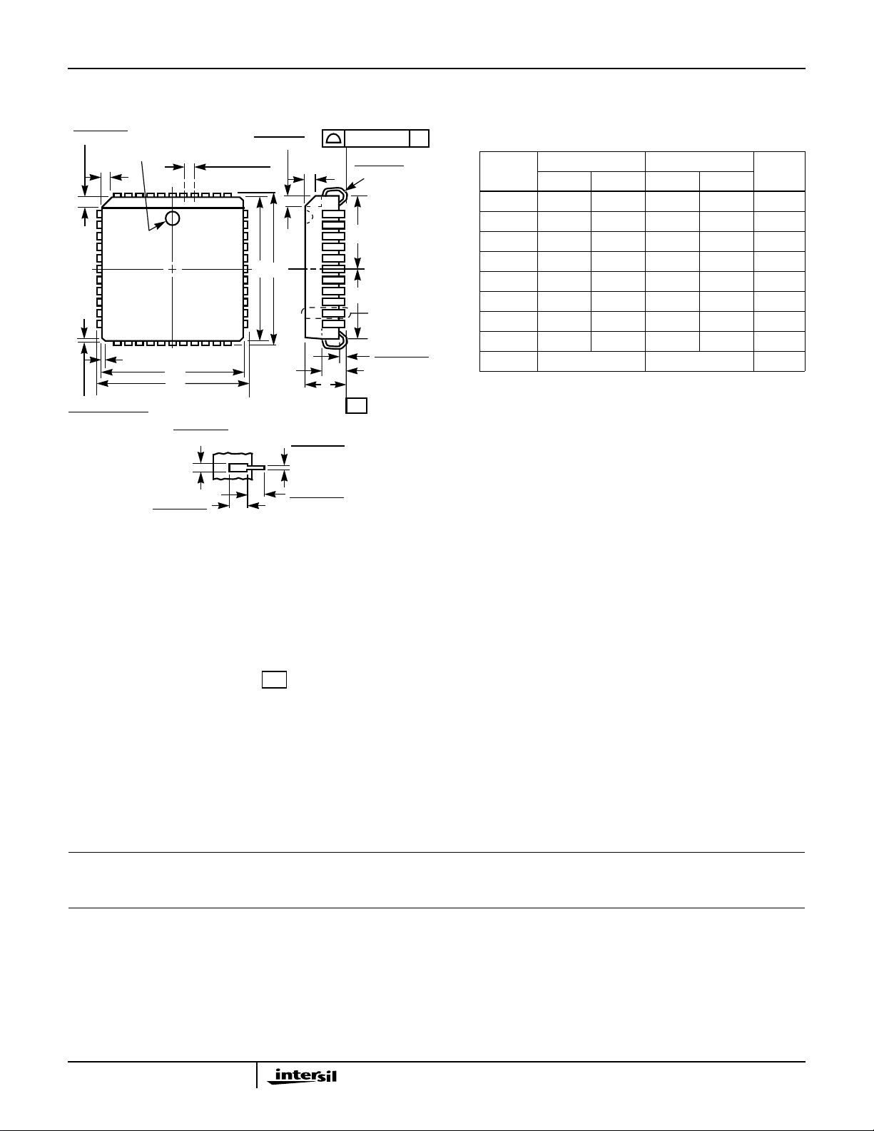
HMU16, HMU17
Plastic Leaded Chip Carrier Packages (PLCC)
0.042 (1.07)
0.048 (1.22)
PIN (1) IDENTIFIER
0.020 (0.51) MAX
3 PLCS
C
L
D1
D
0.026 (0.66)
0.032 (0.81)
0.045 (1.14)
MIN
0.042 (1.07)
0.056 (1.42)
0.050 (1.27) TP
VIEW “A” TYP.
C
L
EE1
0.013 (0.33)
0.021 (0.53)
0.025 (0.64)
MIN
0.004 (0.10) C
0.025 (0.64)
0.045 (1.14)
D2/E2
D2/E2
A1
A
-C-
VIEW “A”
0.020 (0.51)
MIN
SEATING
PLANE
N68.95 (JEDEC MS-018AE ISSUE A)
68 LEAD PLASTIC LEADED CHIP CARRIER PACKAGE
R
SYMBOL
A 0.165 0.180 4.20 4.57 -
A1 0.090 0.120 2.29 3.04 -
D 0.985 0.995 25.02 25.27 D1 0.950 0.958 24.13 24.33 3
D2 0.441 0.469 11.21 11.91 4, 5
E 0.985 0.995 25.02 25.27 E1 0.950 0.958 24.13 24.33 3
E2 0.441 0.469 11.21 11.91 4, 5
N68 686
INCHES MILLIMETERS
NOTESMIN MAX MIN MAX
Rev. 2 11/97
NOTES:
1. Controllingdimension: INCH. Converted millimeterdimensionsare
not necessarily exact.
2. Dimensions and tolerancing per ANSI Y14.5M-1982.
3. DimensionsD1 and E1 do not include mold protrusions. Allowable
mold protrusion is 0.010 inch (0.25mm) per side. Dimensions D1
and E1 include mold mismatch and are measured at the extreme
material condition at the body parting line.
4. To be measured at seating plane contact point.
-C-
5. Centerline to be determined where center leads exit plastic body.
6. “N” is the number of terminal positions.
All Intersil semiconductor products are manufactured, assembled and tested under ISO9000 quality systems certification.
Intersil semiconductor products are sold by description only. Intersil Corporation reserves the right to make changes in circuit design and/or specifications at any time without notice. Accordingly, the reader is cautioned to verify that data sheets are current before placing orders. Information furnished by Intersil is believed to be accurate and
reliable. However,no responsibility is assumed by Intersil or its subsidiaries for its use; nor for any infringements of patents or other rights of third parties which may result
from its use. No license is granted by implication or otherwise under any patent or patent rights of Intersil or its subsidiaries.
For information regarding Intersil Corporation and its products, see web site www.intersil.com
Sales Office Headquarters
NORTH AMERICA
Intersil Corporation
P. O. Box 883, Mail Stop 53-204
Melbourne, FL 32902
TEL: (407) 724-7000
FAX: (407) 724-7240
EUROPE
Intersil SA
Mercure Center
100, Rue de la Fusee
1130 Brussels, Belgium
TEL: (32) 2.724.2111
FAX: (32) 2.724.22.05
ASIA
Intersil (Taiwan) Ltd.
7F-6, No. 101 Fu Hsing North Road
Taipei, Taiwan
Republic of China
TEL: (886) 2 2716 9310
FAX: (886) 2 2715 3029
13
 Loading...