

Datasheet HMS91C7132, HMS91C7132K, HMS91C7134, HMS91C7134K, HMS97C7132 Datasheet (HYNIX)
...Page 1

May. 2001 ver1.1
8-BIT SINGLE-CHIP MONITOR MICROCONTROLLERS
HMS9xC7132
HMS9xC7134
User’s Manual
Page 2

Additional information of this manual may be s erved by HYNIX Semiconductor offices in Korea or Distributors
and Representat ives listed at address di rec tory.
HYNIX Semiconductor reserves the rig ht to make changes to an y information here in at any time without notic e.
The information, diagrams and other data in this manual are correct and reliable; however, HYNIX Semicon-
ductor is in no way respons ible for any violations of patents or other rights of the third party gener ated by the use
of this manu al.
Version 1.1
Published by
MCU Application Team bjinlim@hynix.com blackjoe@ hynix.com
2001 HYNIX Semiconductor All right reserved.
Page 3

HMS9xC7132 / HMS9xC7134
May.2001 ver1.1
1. OVERVIEW . . . . . . . . . . . . . . . . . . . . . . . 1
1.1 Description . . . . . . . . . . . . . . . . . . . . . . . . . . . . . . . .1
1.2 Features . . . . . . . . . . . . . . . . . . . . . . . . . . . . . . . . . .1
2. BLOCK DIAGRAM . . . . . . . . . . . . . . . . . . 2
3. PIN ASSIGNMENT . . . . . . . . . . . . . . . . . 3
3.1 40PDIP pinning . . . . . . . . . . . . . . . . . . . . . . . . . . . .3
3.2 42SDIP pinning . . . . . . . . . . . . . . . . . . . . . . . . . . . .4
4. PACKAGE DIMENSIONS . . . . . . . . . . . . 5
4.1 40 PDIP . . . . . . . . . . . . . . . . . . . . . . . . . . . . . . . . . .5
4.2 42 SDIP . . . . . . . . . . . . . . . . . . . . . . . . . . . . . . . . . .5
5. PIN FUNCTION . . . . . . . . . . . . . . . . . . . . 6
5.1 40DIP Pin Description . . . . . . . . . . . . . . . . . . . . . . .7
5.2 42SDIP Pin Description . . . . . . . . . . . . . . . . . . . . . .8
6. PORT STRUCTURES . . . . . . . . . . . . . . . 9
7. ELECTRICAL CHARACTERISTICS . . . 11
7.1 Absolute Maximum Ratings . . . . . . . . . . . . . . . . . .11
7.2 Recommended Operating Conditions . . . . . . . . . .11
7.3 DC Electrical Characteristics . . . . . . . . . . . . . . . . .11
7.4 AC Characteristics . . . . . . . . . . . . . . . . . . . . . . . . .13
8. MEMORY ORGANIZATION . . . . . . . . . 16
8.1 Registers . . . . . . . . . . . . . . . . . . . . . . . . . . . . . . . .16
8.2 Program Memory . . . . . . . . . . . . . . . . . . . . . . . . . .17
8.3 Data memory . . . . . . . . . . . . . . . . . . . . . . . . . . . . .17
8.4 List of SFRS . . . . . . . . . . . . . . . . . . . . . . . . . . . . . .20
8.5 Addressing Mode . . . . . . . . . . . . . . . . . . . . . . . . . .22
9. INTERRUPTS . . . . . . . . . . . . . . . . . . . . 24
9.1 Interrupt sources . . . . . . . . . . . . . . . . . . . . . . . . . .24
9.2 Interrupt Enable structure . . . . . . . . . . . . . . . . . . .26
9.3 Interrupt Priority structure . . . . . . . . . . . . . . . . . . .27
9.4 How Interrupt are handled . . . . . . . . . . . . . . . . . . .29
10. POWER-SAVING MODE . . . . . . . . . . . 30
10.1 Power control register . . . . . . . . . . . . . . . . . . . . .30
10.2 Idle mode . . . . . . . . . . . . . . . . . . . . . . . . . . . . . . .31
10.3 Power-down mode . . . . . . . . . . . . . . . . . . . . . . . .31
11. I/O PORTS . . . . . . . . . . . . . . . . . . . . . . 32
11.1 Pin function selection . . . . . . . . . . . . . . . . . . . . . .33
12. OSCIALLTOR . . . . . . . . . . . . . . . . . . . 36
13. RESET . . . . . . . . . . . . . . . . . . . . . . . . . 37
13.1 External reset . . . . . . . . . . . . . . . . . . . . . . . . . . . .37
13.2 Watchdog timer overflow . . . . . . . . . . . . . . . . . . .37
13.3 Low VDD voltage reset . . . . . . . . . . . . . . . . . . . .37
14. WATCHDOG TIMER . . . . . . . . . . . . . . 38
15. TIMER . . . . . . . . . . . . . . . . . . . . . . . . . 39
15.1 Timer0 and Timer1 . . . . . . . . . . . . . . . . . . . . . . .39
15.2 TIMER2 . . . . . . . . . . . . . . . . . . . . . . . . . . . . . . . .40
16. DDC INTERFACE . . . . . . . . . . . . . . . . 42
16.1 The SFRs for DDC Interface . . . . . . . . . . . . . . . .43
16.2 DDC1 protocol . . . . . . . . . . . . . . . . . . . . . . . . . . .46
16.3 DDC2B protocol . . . . . . . . . . . . . . . . . . . . . . . . . .46
16.4 DDC2AB/DDC2B+ protocol . . . . . . . . . . . . . . . . .47
16.5 The RAM Buffer and DDC application . . . . . . . . .48
17. I2C INTERFACE . . . . . . . . . . . . . . . . . 51
17.1 The SFRs for I2C Interface . . . . . . . . . . . . . . . . .52
17.2 Programmer’s Guide for I2C and DDC2 . . . . . . .54
18. PULSE WIDTH MODULATION . . . . . . 57
18.1 Static PWM . . . . . . . . . . . . . . . . . . . . . . . . . . . . .57
18.2 Dynamic PWM . . . . . . . . . . . . . . . . . . . . . . . . . . . 58
19. SYNC PROCESSOR . . . . . . . . . . . . . . 60
19.1 Sync input signals . . . . . . . . . . . . . . . . . . . . . . . .60
19.2 Horizontal polarity correcti on . . . . . . . . . . . . . . . .60
19.3 Vertical polarity correction . . . . . . . . . . . . . . . . . .60
19.4 Vertical sync separation . . . . . . . . . . . . . . . . . . . . 60
19.5 Horizontal sync. detection . . . . . . . . . . . . . . . . . . 62
19.6 Vertical sync. detection . . . . . . . . . . . . . . . . . . . .62
19.7 Horizontal sync. generator . . . . . . . . . . . . . . . . . .65
19.8 Vertical sync. generator . . . . . . . . . . . . . . . . . . . .66
19.9 HSYNC / VSYNC output driver . . . . . . . . . . . . . . 66
19.10 Clamp pulse gener ator . . . . . . . . . . . . . . . . . . .67
19.11 Pattern generator . . . . . . . . . . . . . . . . . . . . . . . .67
19.12 Suspend mode . . . . . . . . . . . . . . . . . . . . . . . . . .67
20. AD-CONVERTOR (ADC) . . . . . . . . . . . 71
21. OPERATION MODE . . . . . . . . . . . . . . 73
21.1 OTP MODE . . . . . . . . . . . . . . . . . . . . . . . . . . . . . 73
21.2 64MQFP pinning and Package Dimensions . . . . 78
21.3 64MQFP Pin Description . . . . . . . . . . . . . . . . . . .79
21.4 Development Tools . . . . . . . . . . . . . . . . . . . . . . .81
22. INSTRUCTION SET . . . . . . . . . . . . . . . 82
Page 4

HMS9 xC 7132 / HMS9xC 7134
May.2001 ver1.1
Page 5
HMS9xC7132 / HMS9xC7134
May.2001 ver1.1
1
HMS9xC7132 / HMS9xC7134
CMOS SINGLE-CHIP 8-BIT MICROCONTROLLER
FOR MONITOR
1. OVERVIEW
1.1 Description
The HMS9xC7132/4 is a single-chip microcontroller of the 80C51 family, which is dedicated for monitor application. It is particula r ly
suitable for multi-sync computer monitor controller. This contains DDC interfaces to the PC host, sync-detector and sync-processor for
auto-sync application, ADC, static PWM, dynamic PWM and I
2
C bus i nt erfa ce f or con trol of th e vide o an d de fl ect ion f unc ti ons of th e
monitor.
1.2 Features
• 80C51 core
• 32K bytes of ROM for HMS91C7132/4
(32K bytes of OTP ROM for HMS97C7132/4)
• 256 bytes of RAM and 256 bytes of XRAM for
DDC operation
• Uses an external crystal of 12 MHz
• One DDC compliant interface :
-
Fully supports DDC1 with dedicated hardware
- DDC2B, DDC2AB and DDC2B+ compliant dedicated hardware based on an I
2
C bus interface
- RAM buffer with programmable size, 128 bytes
or 256 bytes, which can be used for DDC operation or shared as system RAM
• On-chip sync processor
-
HSYNC frequency with 12-bit resolution
- VSYNC frequency with 12-bit resolution
- HSYNC and VSYNC polarity
- HSYNC and VSYNC presence detection
- Composite sync separation
- Free running sync. generation
- Clamping pulse output
- Pattern generation
- Separate input for a SOG signal
- Missing pulse insertion option
- HSYNC/ VSYNC change interrupt
• One multi-master/slave I2C interface (up to
400K bit/s) for control of other system IC’s
• Eight 8-bit Static PWM outputs for digital control applications
• Two 8-bit Dynamic PWM outputs for variou s
waveform generation
• One 8-bit ADC with 4 input channels
• LED dri ver port ; two port lines wit h
15 mA drive capability
• One 8-bi t port only for I/O func ti on
• 24 derivative I/O ports configurable for alternative functions
• Watchdog timer (524ms max. )
• On-chip low VDD voltage detect and reset
(reset period: 524ms)
• Operating temperature : 0 to 70
• Special idle and power-down modes with low
power consumption
• Single power supply : 4.5V to 5.5V
Device name ROM Size
RAM
Size
I/O OTP Package
HMS91C7132/4
32K bytes
Mask ROM
512 bytes
30(42DIP)
32(42SDIP)
HMS97C7132/4
40DIP(HMS91C7132/4),
42SDIP(HMS91C7132/4K)
Page 6
HMS9 xC 7132 / HMS9xC7134
2 May.2001 ver1.1
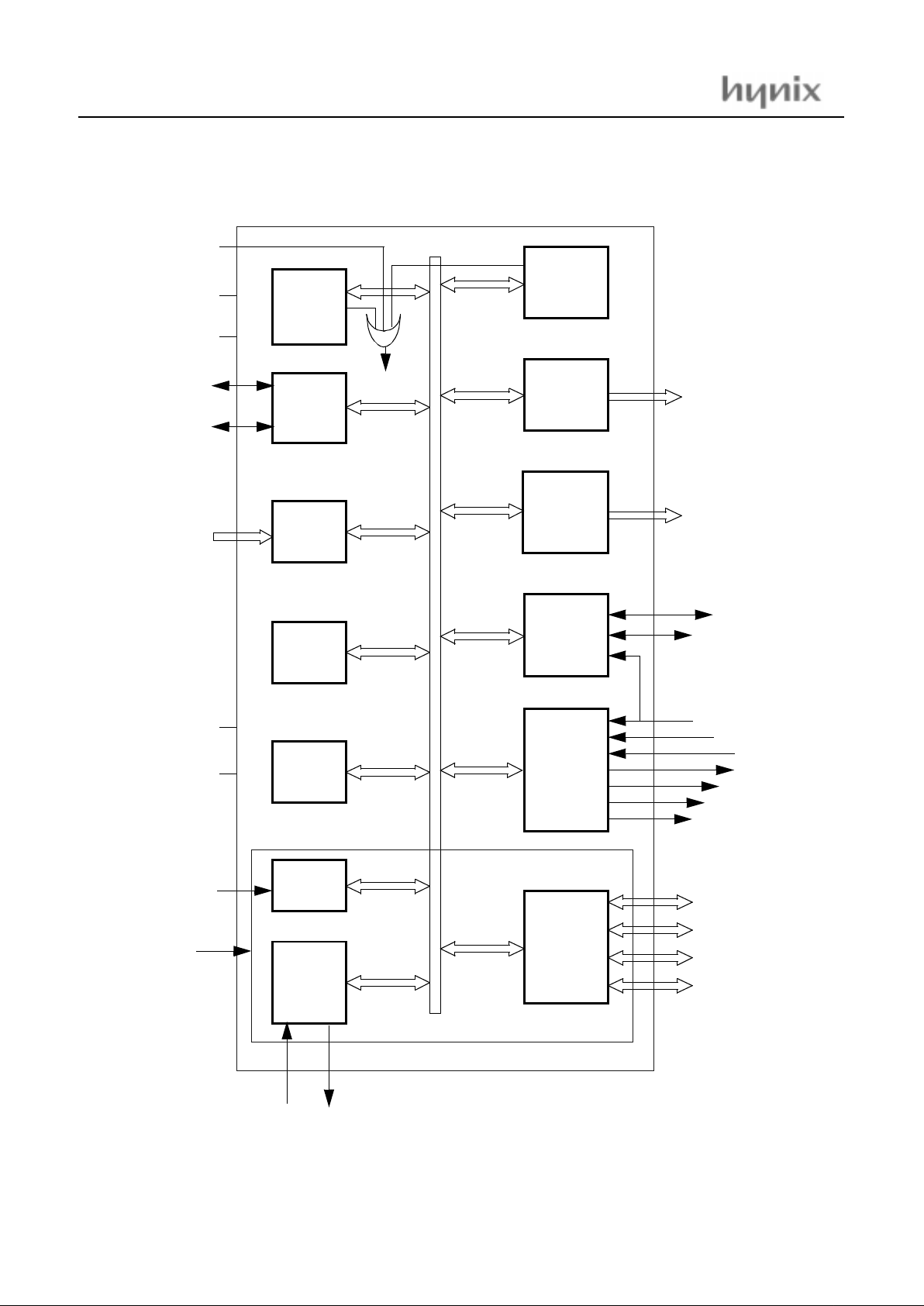
2. BLOCK DIAGRAM
VDD2 VSS2
RESET
SDA2 SCL2
A CH [3:0]
VDD1
VSS1
IN T0
XTAL1
XTAL2
DPWM 0
to
DPWM 1
PW M 0
to
PW M 7
SDA1
SCL1
P 0 P1 P2 P3
PATOUT
CLAMP
HSYNCout
VSYNCout
VSYNCin
HSYNCin
SOGin
Th ree 16-Bit
Ti mers
( T0, T1, T2 )
CPU
Program
Memory
(64KB)
D a ta
Memory
(64KB)
8-Bit
ADC
I2C-Bus
Se rial I/O
Watch Dog
T imer
Pa ra lle l
I/O P orts
&
External Bus
Sy n c . De tec tio n
& S ync. Process
DDC
Interface
8x8-Bit
Sta tic
PW M
2x8-Bit
Dynam ic
PW M
L o w
V o ltag e
R e se t
80C51 core
Page 7
HMS9xC7132 / HMS9xC7134
May.2001 ver1.1
3
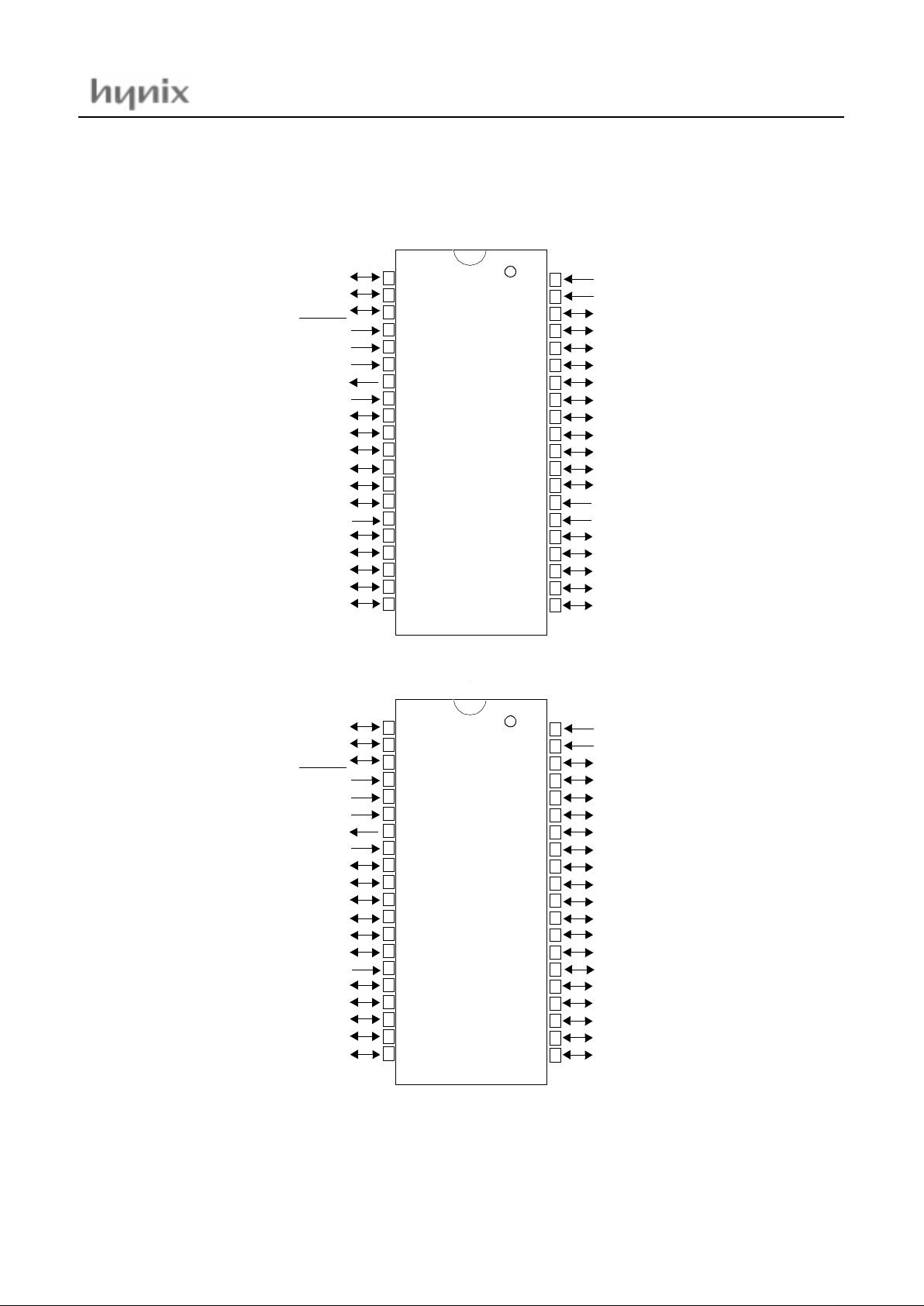
3. PIN ASSIGNMENT
3.1 40PDIP pinning
Vsync-IN
Hsync-IN
PWM1* /P2.3
PWM2* /P2.4
PWM3* /P2.5
PWM4* /P2.6
PWM5* /P2.7
Hsync-OUT /P3.2
Vsync-OUT /P3.3
PWM6* /IN T 1 /P3.4
CLAMP/PWM /P3.5
PADOUT /P3.6
SOG /P3.7
V
DD2
V
SS2
SCL1** /P1.0
SDA1** /P1.1
ACH0 /P1.2
ACH1 /P1.3
ACH2 /P1.4
PWM0* /P2.2
DPWM0* /P2.1
DPWM0* /P2.0
RESET
V
DD1
V
SS1
XTAL2
XTAL1
SDA2** /P1.7
SCL2** /P1.6
P0.7**
P0.6**
P0.5**
P0.4**
INT0/VPP
P0.3**
P0.2**
P0.1**
P0.0**
ACH3 /P1.5
40
39
38
37
36
35
34
33
32
31
30
29
28
27
26
25
24
23
22
21
1
2
3
4
5
6
7
8
9
10
11
12
13
14
15
16
17
18
19
20
HMS9xC7132
* : Open-drain opti on
** : Open-drain type pin
40DIP
(Top View)
Vsync-IN
Hsync-IN
PWM1* /P2.3
PWM2* /P2.4
PWM3* /P2.5
PWM4* /P2.6
PWM5* /P2.7
Hsync-OUT /P3.2
Vsync-OUT /P3.3
PWM6* /INT1 /P3.4/CLAMP
PWM /P3.5
PADOUT /P3.6
SOG /P3.7
P3.0
P3.1
SCL1** /P1.0
SDA1** /P1.1
ACH0 /P1.2
ACH1 /P1.3
ACH2 /P1.4
PWM0* /P2.2
DPWM0* /P2.1
DPWM0* /P2.0
RESET
V
DD1
V
SS1
XTAL2
XTAL1
SDA2** /P1.7
SCL2** /P1.6
P0.7**
P0.6**
P0.5**
P0.4**
INT0/VPP
P0.3**
P0.2**
P0.1**
P0.0**
ACH3 /P1.5
40
39
38
37
36
35
34
33
32
31
30
29
28
27
26
25
24
23
22
21
1
2
3
4
5
6
7
8
9
10
11
12
13
14
15
16
17
18
19
20
HMS9xC7134
* : Open-drain opti on
** : Open-drain type pin
40DIP
(Top View)
Page 8
HMS9 xC 7132 / HMS9xC7134
4 May.2001 ver1.1
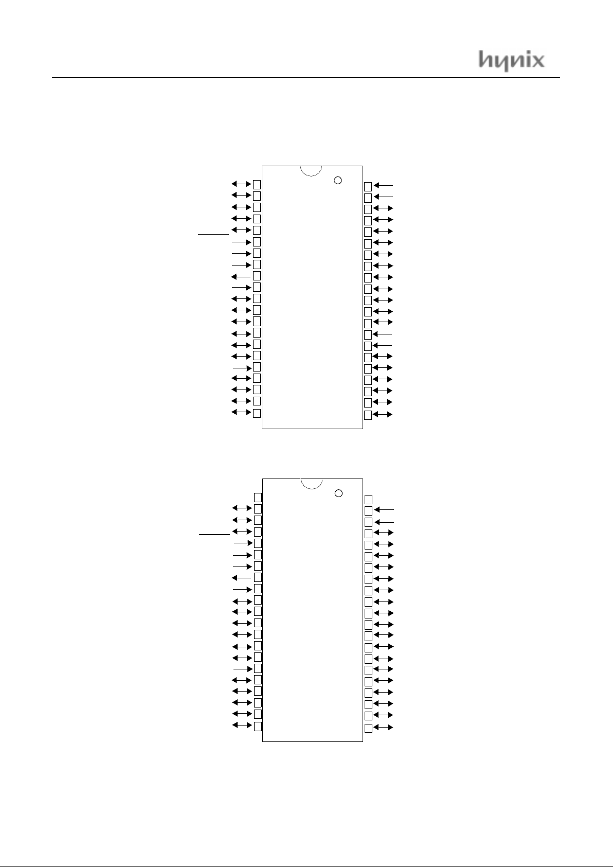
3.2 42SDIP pinning
Vsync-IN
Hsync-IN
PWM1* /P2.3
PWM2* /P2.4
PWM3* /P2.5
PWM4* /P2.6
PWM5* /P2.7
Hsync-OUT /P3.2
Vsync-OUT /P3.3
PWM6* /IN T 1 /P3.4
CLAMP/PWM /P3.5
PADOUT /P3.6
SOG /P3.7
V
DD2
V
SS2
SCL1** /P1.0
SDA1** /P1.1
ACH0 /P1.2
ACH1 /P1.3
ACH2 /P1.4
ACH3 /P1.5
PWM0* /P2.2
DPWM0* /P2.1
DPWM0* /P2.0
P3.1
P3.0
RESET
V
DD1
V
SS1
XTAL2
XTAL1
SDA2** /P1.7
SCL2** /P1.6
P0.7**
P0.6**
P0.5**
P0.4**
INT0/VPP
P0.3**
P0.2**
P0.1**
P0.0**
42
41
40
39
38
37
36
35
34
33
32
31
30
29
28
27
26
25
24
23
22
1
2
3
4
5
6
7
8
9
10
11
12
13
14
15
16
17
18
19
20
21
HMS9xC7132K
* : Open-drain option
** : Open-drain type pin
42SDIP
(Top View)
NC
Vsync-IN
Hsync-IN
PWM1* /P2.3
PWM2* /P2.4
PWM3* /P2.5
PWM4* /P2.6
PWM5* /P2.7
Hsync-OUT /P3.2
Vsync-OUT /P3.3
PWM6* /INT1 /P3.4/CLAMP
PWM /P3.5
PADOUT /P3.6
SOG /P3.7
P3.0
P3.1
SCL1** /P1.0
SDA1** /P1.1
ACH0 /P1.2
ACH1 /P1.3
ACH2 /P1.4
NC
PWM0* /P2.2
DPWM0* /P2.1
DPWM0* /P2.0
RESET
V
DD1
V
SS1
XTAL2
XTAL1
SDA2** /P1.7
SCL2** /P1.6
P0.7**
P0.6**
P0.5**
P0.4**
INT0/VPP
P0.3**
P0.2**
P0.1**
P0.0**
ACH3 /P1.5
42
41
40
39
38
37
36
35
34
33
32
31
30
29
28
27
26
25
24
23
22
1
2
3
4
5
6
7
8
9
10
11
12
13
14
15
16
17
18
19
20
21
HMS9xC7134K
* : Open-drain option
** : Open-drain type pin
42SDIP
(Top View)
Page 9
HMS9xC7132 / HMS9xC7134
May.2001 ver1.1
5
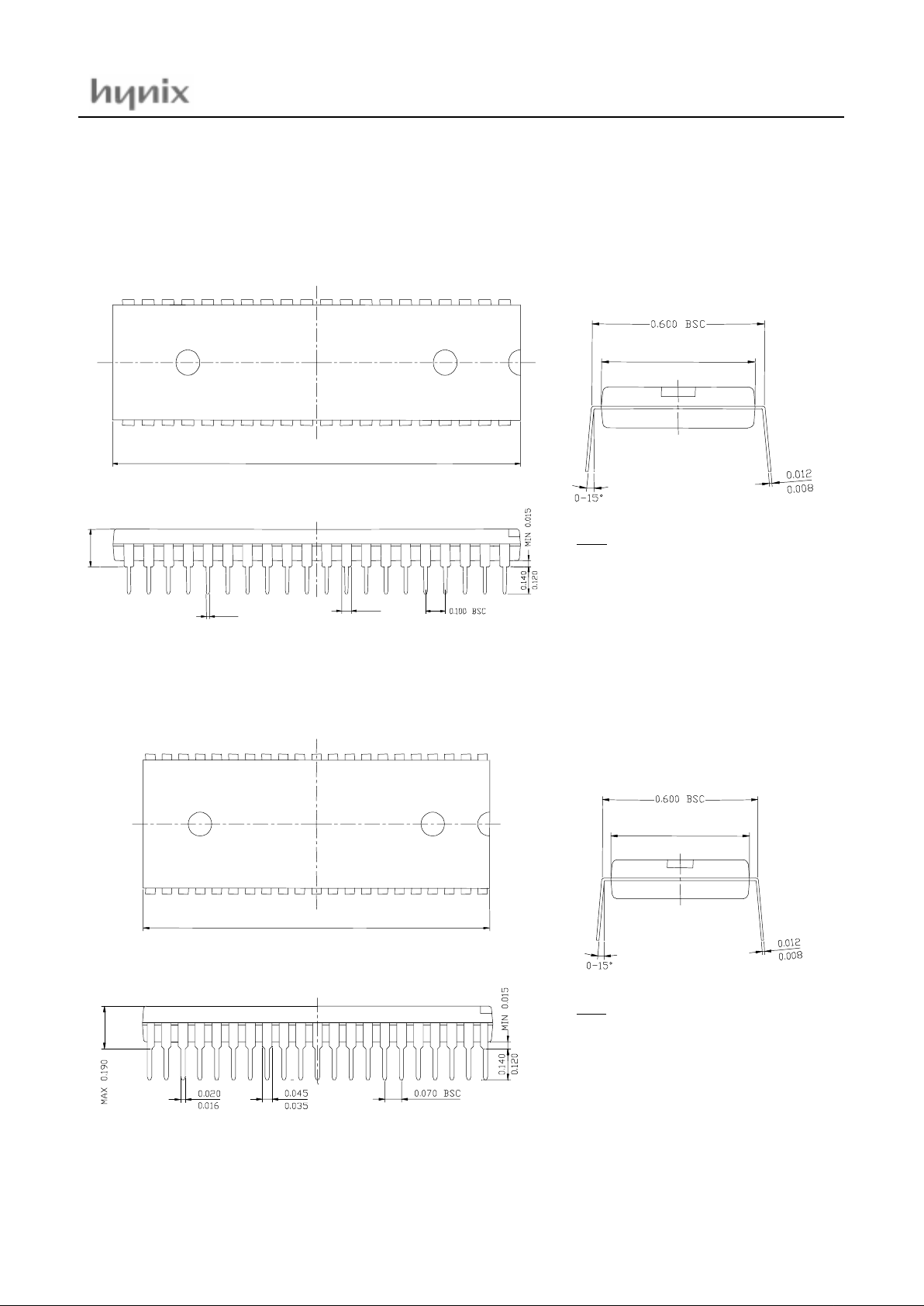
4. PACKAGE DIMENSIONS
4.1 40 PD I P
4.2 42 SD I P
2.075
2.045
MAX 0.200
0.022
0.015
0.065
0.045
NOTE
1. DIMENSIONS DO NOT INCLUDE MOLD
FLASH AND DAMBAR PROTRUSION.
ALLOWABLE MOLD FLASH IS 0.010 INCH.
2. CONTROLLING DIMENSION : INCH.
0.550
0.530
1.470
1.450
NOTE
1. DIMENSIONS DO NOT INCLUDE MOLD
FLASH AND DAMBAR PROTRUSION.
ALLOWABLE MOLD FLASH IS 0.010 INCH.
2. CONTROLLING DIMENSION : INCH.
0.550
0.530
Page 10

HMS9 xC 7132 / HMS9xC7134
6 May.2001 ver1.1
5. PIN FUNCTION
V
DD1
: Supply voltage (Di gital).
V
SS1
: Circuit ground (Digital).
V
DD2
: Supply vo ltage (Analog).
V
SS2
: Circuit ground (Analog).
RESET
: Reset the MCU.
XTAL1
: Input to the inverting oscillator amplifier and input to
the internal main clock operating circuit.
XTAL2
: Output from the invert ing oscill ator amplifi e r.
HSYNC
IN
: Horizo ntal sync input
VSYNC
IN
: Vertical sync input
INT0/V
PP
: External Interrupt input. Programming supply volt-
age(during O TP programming)
PORT:
The HMS9xC7132 has four 8-bit ports (Port0, Port1, Port2,
and Port3). Port0 - Port3 are the same as in the 80C51, with
the exception of the additional functions of Port1, Port2 and
Port3. Each has latch, SFR P0~P3’ output driver and input
buffer.
P0.0~P0.7
: P0 is an 8-bit CMOS bidirectional I/O port. P0 pins
have not pull -up res iste r a nd open- dr ain port. It has th e ca pabi lit y
of drive LED. How ever, while the alternative function is performed, th e por t type w ill remai n th e same. In ca se of appli cat ion
to extention of external memory, P0 outputted Write/Read byte
and lower byt e of external memory address. Therefore when it is
used as normal I/O port, P0 is open-d rain driver and when it used
as bus port, P0 is 3-state driver.
P1.0~P1.7
: P1 is an 8-bit CMOS bidirectional I/O port. Because
P1 pins have pull-up resister, it is called as Quasi-Bidirectional
port.
P2.0~P2.7
: P2 is an 8-bit CMOS bidirectional I/O por t. Because
P2 pins have pull-up resister, it is called as Quasi-Bidirectional
port. .
P3.0~P3.7
: P3 is an 8-bit CMOS bidirectional I/O por t. Because
P3 pins have pull-up resister, it is called as Quasi-Bidirectional
port.
Port pin Alternate funct ion
P0.0
P0.1
P0.2
P0.3
P0.4
P0.5
P0.6
P0.7
No (Only for I/O functi on)
No (Only for I/O functi on)
No (Only for I/O functi on)
No (Only for I/O functi on)
No (Only for I/O functi on)
No (Only for I/O functi on)
No (Only for I/O functi on)
No (Only for I/O functi on)
Port pin Alternate function
P1.0
P1.1
P1.2
P1.3
P1.4
P1.5
P1.6
P1.7
SCL1 (DDC-SCL)
SDA1 (DDC-SDA)
ACH0
ACH1
ACH2
ACH3
SCL2 (I
2
C-SCL)
SDA2 (I
2
C-SDA)
Port pin Alternate function
P2.0
P2.1
P2.2
P2.3
P2.4
P2.5
P2.6
P2.7
DPWM0*
DPWM1*
PWM0*
PWM1*
PWM2*
PWM3*
PWM4*
PWM5*
Port pin Alternate function
P3.0
P3.1
P3.2
P3.3
P3.4
P3.5
P3.6
P3.7
Reserved
Reserved
HSYNC
OUT
VSYNC
OUT
PWM6*
CLAMP/PWM7
PATOUT
SOG
Page 11
HMS9xC7132 / HMS9xC7134
May.2001 ver1.1
7
5.1 40DIP Pin Description
PIN NAME
(Alternate)
Pin
No.
In/Out
(Alter-
nate)
Function
Basic Alternate
PWM0 /P2.2 1 I/O General I/O port P2.2 8-bit Pulse Width Modulation output0
DPWM0 /P2.1 2 I /O General I/O port P2.1 8-bit Dynamic Pulse Width Modulation output0
DPWM0 /P2.0 3 I /O General I/O port P2.0 8-bit Dynamic Pulse Width Modulation output1
RESET
4 I Reset input
V
DD1
5 - Power supply1(+5V)
V
SS1
6 - Ground1
XTAL2 7 O Oscillat or out put pin for system clock
XTAL1 8 I Oscillator input pin f or system clock
SDA2 /P1.7 9 I/O General I/O port P1.7
I2C serial data I/O port
SCL2 /P1.6 10 I/O General I/O port P1.6
I
2
C serial clock I/O port
P0.7 11 I/O Gen eral I/O port P0.7; adapted for LED driver
P0.6 12 I/O Gen eral I/O port P1.6; adapted for LED driver
P0.5 13 I/O General I/O port P0.5
P0.4 14 I/O General I/O port P0.4
INT0 /V
PP
15 I External interrupt input 0; Pr ogramming supply voltage ( duri ng OTP programming)
P0.3 16 I/O General I/O port P0.3
P0.2 17 I/O General I/O port P0.2
P0.1 18 I/O General I/O port P0.1
P0.0 19 I/O General I/O port P0.0
ACH3 /P1.5 20 I/O General I/O port P1.5 ADC channel3 input
ACH2 /P1.4 21 I/O General I/O port P1.4 ADC channel2 input
ACH0 /P1.3 22 I/O General I/O port P1.3 ADC channel1 input
ACH0 /P1.2 23 I/O General I/O port P1.2 ADC channel0 input
SDA1 /P1.1 24 I/O General I/O port P1.1
I
2
C serial data I/O port for DDC interf ace
SCL1 /P1.0 25 I/O General I/O port P1.0
I
2
C serial clock I/O port for DDC interface
V
SS2
26 - Ground2
V
DD2
27 - Power supply2(+5 V)
SOGin /P3.7 28 I/O General I/ O port P3.7 Sync on Green input
PATOUT /P3.7 29 I/O General I/O port P3.6 Pattern out
CLAMP /PWM7 /
P3.5 /PR O G
30 I/O
General output only port P3.5
Program pulse input(during OTP
programming)
Clamp out ; 8-bit Pulse Widt h Modu lation
output7
PWM6 /P3.4 /
INT1
31 I/O General I/O port P3.4
8-bit Pulse Width Modu lat ion output6; External
interrupt input 1
VSYNCout /P3.3 32 I/O General I/O port P3.3 Vertical sync output
HSYNCout /P3.2 33 I/O General I/O port P3.2 Horizontal sync output
PWM5 /P2.7 34 I/O General I/O port P2.7 8- bit Pulse Width Modulation output5
PWM4 /P2.6 35 I/O General I/O port P2.6 8- bit Pulse Width Modulation output4
PWM3 /P2.5 36 I/O General I/O port P2.5 8- bit Pulse Width Modulation output3
PWM2 /P2.4 37 I/O General I/O port P2.4 8- bit Pulse Width Modulation output2
Table 5-1 Port Function Descri ption(40DIP)
Page 12

HMS9 xC 7132 / HMS9xC7134
8 May.2001 ver1.1
5.2 42SDIP Pin Description
The 42SDIP type pin description is the same as The 40DIP type pin description except for adding two pins(P3.1, P3.0) to it
between pin no.4 and 5.
PWM1 /P2.3 38 I/O General I/O port P2.3 8-bit Pulse Width Modulation output1
HSYNCin 39 I Horizontal sync input
VSYNCin 40 I Vertical sync input
PIN NAME
(Alternate)
Pin
No.
In/Out
(Alter-
nate)
Function
Basic Alternate
Table 5-1 Port Function Descri ption(40DIP)
Page 13
HMS9xC7132 / HMS9xC7134
May.2001 ver1.1
9
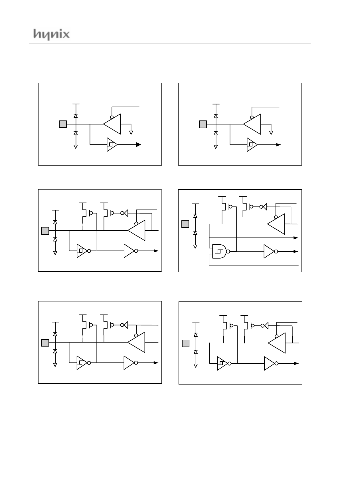
6. PORT STRUCTURES
P0.0 - P0.5 P0.6 - P0.7
P1.0, P1.1, P1.6, P1.7, P2.0~7, P3.0, P3.1, P3.4, P3.6 P1.2 - P1.5
P3.2, P3 .3, P3.5 P3.7
data
CMOS
5mA
data
CMOS
10mA
oen
data
CMOS
adc_enb
oen
data
adc_in
CMOS
internal reset
data
TTL
oen
data
TTL
Page 14
HMS9 xC 7132 / HMS9xC7134
10 May.2001 ver1.1
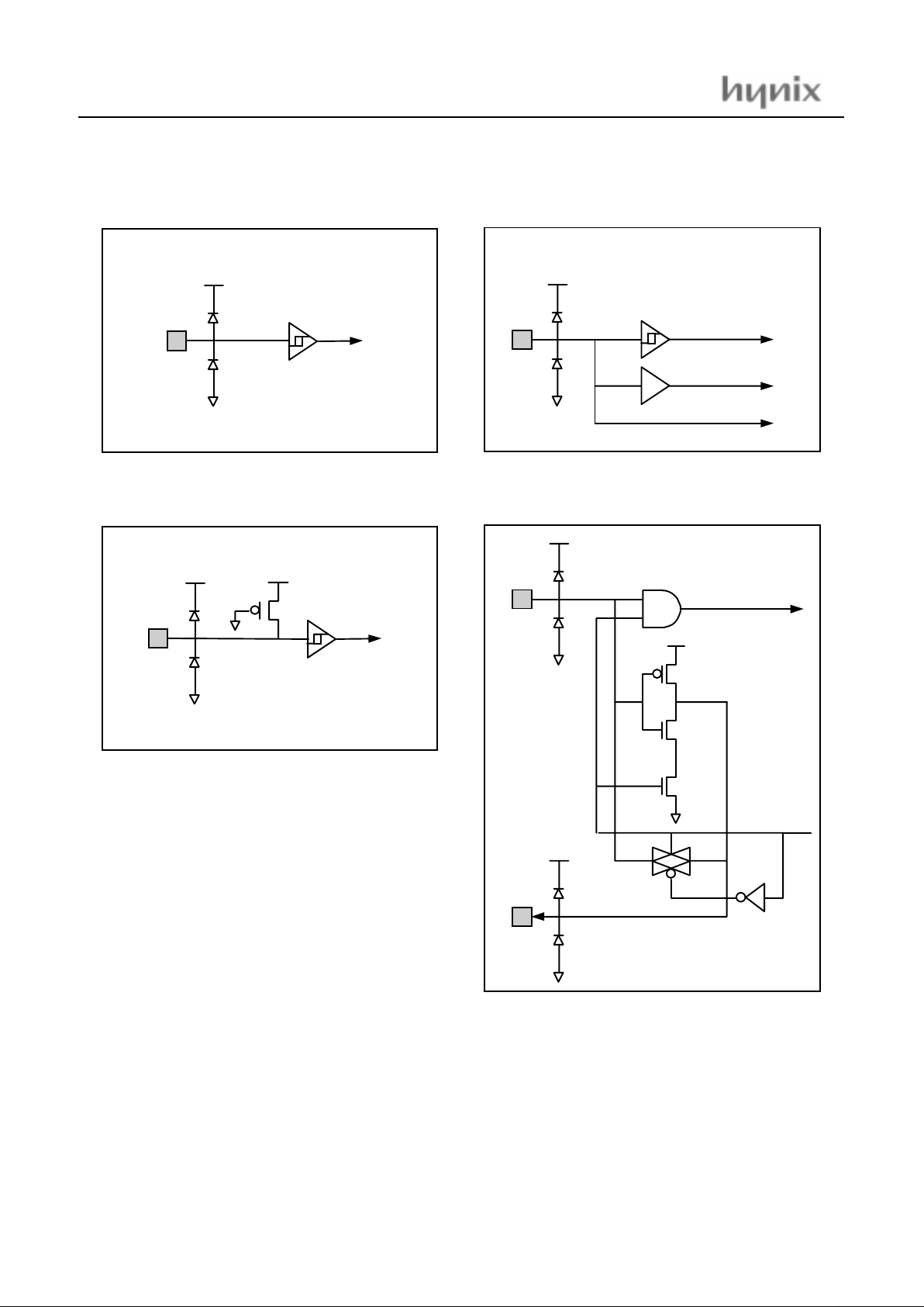
HSYNCIN, VSYNCIN INT0/VPP
RESET XTAL1, XTAL2
TTL
H
TTL
VPP detector
VPP
CMOS
pdb
Page 15
HMS9xC7132 / HMS9xC7134
May.2001 ver1.1
11
7. ELECTRICAL CHARACTERISTICS
7.1 Absolute Maximum Ratings
Supply voltage......................................................-0.5 to +6.5 V
Storage Temperature .......................................... -65 to +150 °C
Voltage on any pin with respect to Ground (V
SS
)
..........................................................................-0.5 to V
DD
+0.5
Note: Stresses above those listed under "Absolute Maxi-
mum Ratings" may cause pe rmanent dam age to the device. This is a stress rating only and functional operation of
the device at a ny other conditio ns above those indicated in
the operational sections of this specification is not implied.
Exposure to abso lute maximum rati ng conditions for extended periods may aff ect device reliability.
7.2 Recommended Operating Conditions
7.3 DC El ectrical Char acteristics
(TA= 0~70°C, VDD=4.5~5.5V, VSS=0V )
,
Parameter Symbol Condition
Specifications
Unit
Min. Max.
Supply Voltage
V
DD
f
XIN
=12MHz
4.5 5.5 V
Operating Frequency
f
XIN
VDD=4.5~5.5V
10 16 MHz
Operating Temperature
T
OPR
-070
°
C
Symbol Parameter Condition
Specifications
Unit
Min. Typ. Max.
SUPPLY
VDD power supply volt age - 4.5 5.0 5.5 V
IDD power suppl y current Fosc - 12MHz
-
TBD
-
mA
VLVR low voltage reset - 3.3 3.7 4.1 V
OTP SUPPLY
VDD power supply volt age - 4.5 5.0 5.5 V
VPP programming voltage - - 12.75 - V
IDDP power supply current Fosc - 4MHz
-
TBD
-
mA
IPP programming current Fosc - 4MHz
-
TBD
-
mA
RESET
IRST RESET input pull-up resistance VIN - 0V
-
33 -
µ
A
IIH input leakage current VIN - VDD
-
01µA
VIL1 LOW-level input volt age - VSS-0.5 - 0.3VDD V
VIH1 HIGH-level input volt age - 0.7VDD - VDD+0.5 V
XTAL
VOP open bias voltage - - 2.5 - V
IFR feedback resistor current VIN - 5V - 10 -
µ
A
VIL1 LOW-level input volt age - VSS-0.5 - 0.3VDD V
VIH1 HIGH-level input volt age - 0.7VDD - VDD+0.5 V
INT0, HSYNCIN, VSYNCIN
IIL input leakage current VIN - VSS -1 0 -
µ
A
IIH input leakage current VIN - VDD - 0 1
µ
A
VIL LOW-level input voltage - VSS-0.5 - 0.3VDD V
Page 16
HMS9 xC 7132 / HMS9xC7134
12 May.2001 ver1.1
VIH HIGH-level input voltage - 2.0 - VDD+0.5 V
SOG/P3.7
IIL1 input leakage current VIN - 0.45V -55 - -10
µ
A
ITL input transition current VIN - 2.0V -650 - -65
µ
A
IIH input lea kage current VIN - VDD - 0 1
µ
A
VIL LOW-level input voltage - VSS-0.5 - 0.8 V
VIH HIGH-level input voltage - 2.0 - VDD+0.5 V
VOL LOW-level output vol ta ge IOL - 5mA 0 - 0.4 V
VOH HIGH-level input voltage IOH - 5mA 3.5 - VDD V
P0.0 to P0.5
IIL input leakage current VIN - VSS -1 0 -
µ
A
IIH input lea kage current VIN - VDD - 0 1
µ
A
VIL1 LOW-level i nput voltage - VSS-0.5 - 0.3VDD V
VIH1 HIGH-level input voltage - 0.7VDD - VDD+0.5 V
VOL LOW-level output vol ta ge IOL - 5mA 0 - 0.4 V
P0.6 to P0.7
IIL input leakage current VIN - VSS -1 0 -
µ
A
IIH input lea kage current VIN - VDD - 0 1
µ
A
VIL1 LOW-level i nput voltage - VSS-0.5 - 0.3VDD V
VIH1 HIGH-level input voltage - 0.7VDD - VDD+0.5 V
VOL1 LOW-level output voltage IOL - 10mA 0 - 0.4 V
P2.0 to P2.7(BP2.0 to BP2.7)
IIL1 input leakage current VIN - 0.45V -55 - -10
µ
A
ITL1 input transition current VIN - 3.5V -650 - -65
µ
A
IIH input lea kage current VIN - VDD - 0 1
µ
A
VIL1 LOW-level i nput voltage - VSS-0.5 - 0.3VDD V
VIH1 HIGH-level input voltage - 0.7VDD - VDD+0.5 V
VOL LOW-level output vol ta ge IOL - 5mA 0 - 0.4 V
VOH HIGH-level input voltage IOH - 5mA 3.5 - VDD V
P1.0 to P1.7,P3.0,P3.1,P3.4,P3.6,P3.7
IIL1 input leakage current VIN - 0.45V -55 - -10
µ
A
ITL1 input transition current VIN - 3.5V -650 - -65
µ
A
IIH input lea kage current VIN - VDD - 0 1
µ
A
VIL1 LOW-level i nput voltage - VSS-0.5 - 0.3VDD V
VIH1 HIGH-level input voltage - 0.7VDD - VDD+0.5 V
VOL LOW-level output vol ta ge IOL - 5mA 0 - 0.4 V
VOH HIGH-level input voltage IOH - 5mA 3.5 - VDD V
P3.2 to P3.3,P3.5
IIL2 input leakage current VIN - 0.45V -960 -320
µ
A
ITL2 input transiti on current VIN - 2.0V -1240 -350
µ
A
IIH input lea kage current VIN - VDD 0 1
µ
A
VIL LOW-level input voltage - VSS-0.5 0.8 V
VIH HIGH-level input voltage - 2.0 VDD+0.5 V
Symbol Parameter Condition
Specifications
Unit
Min. Typ. Max.
Page 17
HMS9xC7132 / HMS9xC7134
May.2001 ver1.1
13
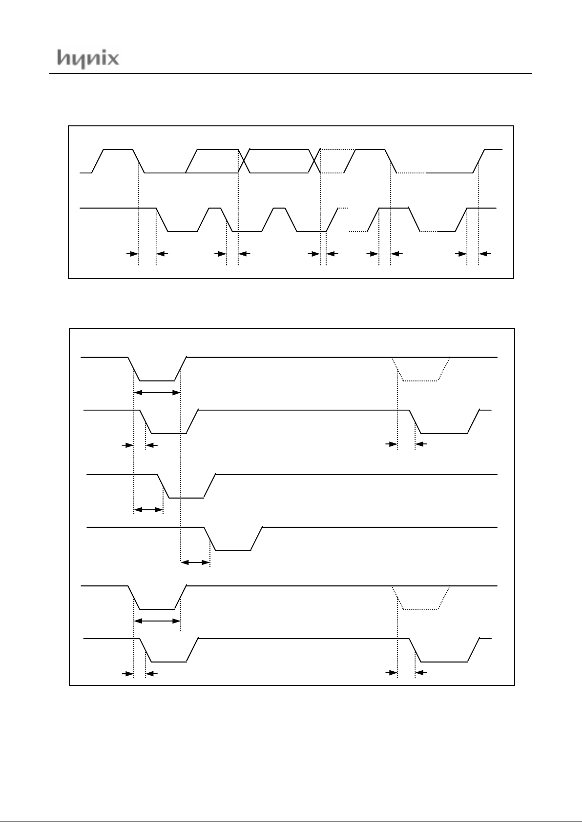
7.4 AC Characteristics
(TA=-0~70°C, VDD=5.0V, VSS=0V)
VOL LOW-level output voltage IOL - 5mA 0 0.4 V
VOH HIGH-level input voltage IOH - 5mA 3.5 VDD V
Symbol Parameter Condition
Specifications
Unit
Min. Typ. Max.
Symbol Parameter Condition
Specifications
Unit
Min. Typ. Max.
XTAL
fosc oscillator frequency VDD - 5V 10 12 16 MHz
C1 xtal1 external Cap. - - 20 - pF
C2 xtal2 external Cap. - - 20 - pF
A/D Converter
V
AIN
analog input voltage - VSS - VDD V
n
AOFF
zero offset error - - - TBD LSB
n
FS
full scale error - - 20 TBD LSB
n
ACC
overall acc uracy - - - TBD LSB
t
CONV
conversion tim e fosc - 12MHz - 13 -
µ
s
DDC1 Mode
t
H(VCLK)
VCLK high time - 20 - -
µ
sV
t
L(VCLK)
VCLK low time - 20 - -
µ
s
t
DOV
VCLK to output valid fosc - 12MHz - - 680
µ
s
t
SU(DDC1)
DDC1 mode setup time - - TBD -
µ
s
t
NC(IN)
cancelled noi se input fosc - 12MHz - - 300
µ
s
DDC2 Mode
f
SCL
SCL clock frequency - 0 - 100 kHz
t
HD(SDA)
Start condition hold time - 4.0 - -
µ
s
t
SU(STO)
Stop conditi on setup time - 4.0 - -
µ
s
t
HD(DAT)
Data hold time - 300 - -
µ
s
t
SU(STA)
Rstart(1) condition setup time - 4.7 - -
µ
s
t
H(SCL)
SCL high period - 4.0 - -
µ
s
t
L(SCL)
SCL low period - 4.7 - -
µ
s
HSYNCin
f
(HSYNC)
HSYNC input frequency - 12 - 120 kHz
t
W(HSYNC)
HSYNC input pulse width - 0.25 - 8
µ
s
d
(HSYNC)
HSYNC duty cycle - - - 25
%
VSYNCin
f
(VSYNC)
VSYNC input frequency - 32 - 200 Hz
t
W(VSYNC)
VSYNC input pulse width - 1 - 24
t
P(H)
d
(VSYNC)
VSYNC duty cycle - - - 25
%
SOGin
Page 18
HMS9 xC 7132 / HMS9xC7134
14 May.2001 ver1.1
t
P(EQ)
equalizing pulse period - - 0.5 -
t
P(H)
t
W(EQ)
equalizing pulse widt h - - 0.5 -
t
W(H)
n
(EQ)
equalizing pulse interval - - - 30
t
P(H)
HSYNCout, VSYNCout
t
D(HSYNC)
HSYNC input to output - - - 100 ns
t
D,MAX(HSYNC)
HSYNC input to output
after missing HSYNCin
- - - 250 ns
t
D(HSYNC)
VSYNC input to output - - - 180 ns
t
D,MAX(VSYNC)
VSYNC input to output
after missing VSYNCin
---1
t
P(H)
t
D(CLAMP)
HSYNCin to CLAMP - - - 100 ns
Symbol Parameter Condition
Specifications
Unit
Min. Typ. Max.
Page 19
HMS9xC7132 / HMS9xC7134
May.2001 ver1.1
15
Figure 7-1 timing on the I2C- bus
Figure 7-2 SYNC timing
SDA
SCL
t
HD(SDA)
t
HD(DAT)
t
SU(DAT)
t
SU(STA)
t
SU(STO)
HSYNCin
HSYNCout
t
D(HSYNC)
t
D,MAX(HSYNC)
t
W(HSYNC)
CLAMP
(front porch)
t
D(CLAMP)
t
D(CLAMP)
CLAMP
(back porch)
VSYNCin
VSYNCout
t
D(VSYNC)
t
D,MAX(VSYNC)
t
W(VSYNC)
Page 20
HMS9 xC 7132 / HMS9xC7134
16 May.2001 ver1.1
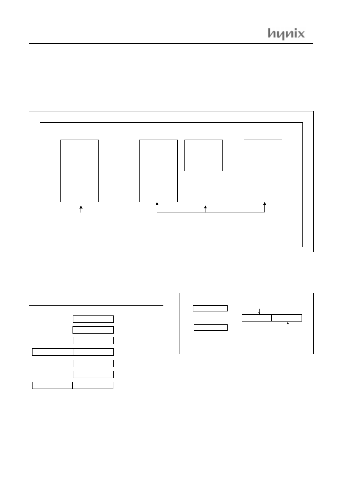
8. MEMORY ORGANIZATION
The HMS91C7132 has separate address spaces for Program
memory, Data Memory. Program memory can only be read, not
written to. It can be up to 32K bytes of Program memory.(OPT
type: HMS97C7132 32K bytes)
Data memory can be read and written to up to 256 bytes including
the stac k area.(In ternal R AM) and 256b ytes (Ex ternal RAM :
256bytes of XRAM0).
Figure 8-1 Memory map and address spaces
8.1 Registers
This device has several registers that are the Program Counter
(PC), A cc umul at or (A) , B regis te r( B), t he St ack P o inte r ( SP ), th e
Program Status Word(PSW), General purpose register(R0~R7)and DPTR(Data poi nter register).
Figure 8-2 Configuration of Registers
Accumulator:
The Accumu lator is the 8-bit gen eral pur pose reg-
ister, used for data operation such as transfer, temporary saving,
and condit ional judgement, etc. Th e A ccumulator can be used as
a 16-bit register with B Register as shown below.
Figure 8-3 Configuration of BA 16-bit Registers
B Register:
The B Regi ster is the 8-bit pu rpose register, used for
an arithm atic ope ration su ch as multi p ly, division with A ccumulator
Stack Pointer
: The Stack Pointer is an 8-bi t register used for occurrence interrupts and calling out subroutines. Stack Pointer
identifies the location in the stack to be access (save or restore).The stack can be located at any position within 0000
H
to
007F
H
of the internal data memory. The SP is not initialized by
hardware, requiring to write the initial value (the location with
32K ROM
Indirec t
only
(“mov @ri”)
Direct(“m ov”)
or Indirect
(“mov @ri”)
0
127
255
Direct
(“mov”) or
Indirect
(“mov @ri” )
Indirect
(“movx @ri” or
movx @dptr)
(XRAMS = 0)
data memoryprogram memory
SFR XRAMRAM
A
ACCUMULATOR
STACK POINTER
PROGRAM COUNTER
PROGRAM STATUS
WORD
SP
PCLPCH
PSW
R0~R7
GENERAL PURPOSE
B
B REGISTER
REGISTER (BANK0~3)
DPTR(DPL)DPTR(DPH)
DATA POINTER
REGISTER
Two 8-bit Registers can be used as a "BA" 16-bit Register
B
A
B A
Page 21
HMS9xC7132 / HMS9xC7134
May.2001 ver1.1
17
which the use of the stack starts) by using the initialization routine. Normally, the initial value of “07
H
” is used and the stack
area is 00
H
to 7FH .
Program Counter
: The Program Counter is a 16-bit wide which
consists of two 8-bit registers, PCH and PCL. This counter indicates the address of the next instruction to be executed. In reset
state, the program counter has reset routine address (PC
H
:0FFH,
PC
L
:0FEH).
Program Status Word
: The Program Status Word (PSW) contains several bits that reflect the cur rent stat e of the CPU an d select Internal RAM(00H~1FH:Bank0~Bank3). The PSW is
described in Figure 8-4. It contains the Carry flag, the Auxiliary
carry flag, the Half Carry (for BCD operation), the General purpose flag, the Register bank select flags, the Overflow flag, the
undefine d flag and Parity flag.
[Carry flag CY]
This flag stores any carry or not borrow from the ALU of CPU
after an arithmetic operation and is also changed by the Shift Instruction or Rotate Instruction.
[Auxiliary carry flag AC]
After operation, this is set when there is a carry from bit 3 of ALU
or there is no borrow from bit 4 of ALU.
[Register bank select flags RS0, RS1]
This flags s elect one of four bank(0 0~07H:b ank0, 08~ 0fH:bank 1,
10~17H:bank2, 17~1FH:bank3)in Internal RAM.
[Overflow flag OV]
This flag is set to “1” when an overflow occurs as the result of an
arithmetic operation involving signs. An overflow occurs when
the result of an addition or subtraction exceeds +127(7F
H
) or -
128(80
H
). The CL R V in structio n cl ea rs the ov er fl ow flag. There
is no set instruction. When the BIT instruction is executed, bit 6
of memor y is cop i ed to th is flag.
[Parity flag P]
This flag r ef lect on nu mber of Accu mula to r’s 1. I f num ber of Ac-
uumulator’s 1 is odd, P=0. otherwise P=1. Sum of adding Acuumulator’s 1 to P is always even.
R0~R7
: Genera l purpos e re gister.
Data Pointer Register
:Data Pointer Register is 16-bit wide
which consi sts of two- 8bit re gi st ers, DPH an d DPL. This re gi st er
is used as a d ata pointer for the data transmission with external
data memory.
Figure 8-4 PSW(Program Stat us Wo rd)Register
8.2 Program Memory
The program memory consists of ROM : 32K bytes (HMS91C7132) and 32K bytes (HMS97C7132)
8.3 Data memory
The inte rnal data memory is d ivided into four phys ically sep arated part : 256 bytes of RAM, 256 byte s of XRAM0 , and 128 by te s
of Special Function Registers (SFRs) areas.
RAM
Four register banks, each 8 registers wide, occupy locations 0
through 3 1 in the lower RAM area. Only one of the se banks may
be enabled at a time. The next 16 bytes, locations 32 through 47,
SP
00
H
Stack Area (30H ~ 7FH)
Bit 15 Bit 087
Hardware fixed
00H~7F
H
SP (Stack Pointer) could be in 00H~7FH.
CARRY FLAG
MSB
LSB
RESET VALUE: 00
H
PSW
AUXILIARY CARRY FLAG
REGISTER BANK SELECT FLAG
PARITY FLAG
NOT ASSIGNED BIT
OVERFLOW FLAG
REGISTER BANK SELECT FLAG
GENERAL PURPOSE FLAG
CY AC F0 RS1 RS0 0V P
(to select Bank0~3 with RS0)
(to select Bank0~3 with RS1)
Page 22
HMS9 xC 7132 / HMS9xC7134
18 May.2001 ver1.1
contain 128 directly addressable bit locations.The stack depth is
only limited by the available internal RAM space of 256 bytes.
XRAM0
The 256 bytes of XRAM0 used to support DDC interface is also
available fo r sys tem usa ge by ind irec t addr essi ng thr ou gh the address pointer DDCADR and data I/O buffer RAMBUF. The address pointer(D DCADR ) is e quippe d with the po stincre ment
capability to facilitate the transfer of data in bulk (for details refer
to DDC I nte rfac e p ar t) . H oweve r, it is a ls o poss ibl e to ad dre ss th e
DRAM through MOVX command as usually used in the internal
RAM extensi on of 80C51 de ri va tives . XRAM0 0 to 255 is di rect ly addressable as external data memory locations 0 to 255 via
MOVX-DPTR instruction or via MOVX-Ri instruction when the
EXCON’s LSB is zero. S ince exte rnal acc ess func tion is n ot
available, any ac cess to XRAM 0 0 to 255 w ill not affect the
ports.
7 6 5 4 3 2 1 0
Table 8-1 Extended control Register(EXCON)
Figure 8-5 RAM ADDRESS
-------
XRAMS
BANK 3
BANK 2
BANK 1
BANK 0
00H
07H
08H
0FH
10H
17H
1FH
18H
2FH
2EH
2DH
2CH
2BH
2AH
29H
28H
27H
26H
25H
24H
23H
22H
21H
20H
FFH
0
7
8
15
16
23
31
24
47
46
45
44
43
42
41
40
39
38
37
36
35
34
33
32
255
(MSB)
(LS B)
1F 1E 1D 1C 1B 1A 19 18
17 16 15 14 13 12 11 10
0F 0E 0D 0C 0B 0A 09 08
07 06 05 04 03 02 01 00
3F 3E 3D 3C 3B 3A 39 38
37 36 35 34 33 32 31 30
2F 2E 2D 2C 2B 2A 29 28
27 26 25 24 23 22 21 20
5F 5E 5D 5C 5B 5A 59 58
57 56 55 54 53 52 51 50
4F 4E 4D 4C 4B 4A 49 48
47 46 45 44 43 42 41 40
7F 7E 7D 7C 7B 7A 79 78
77 76 75 74 73 72 71 70
6F 6E 6D 6C 6B 6A 69 68
67 66 65 64 63 62 61 60
~
~
BYTE
ADDRESS
(HEX)
BIT
ADDRESS
(HEX )
BYTE
ADDRESS
(DECIMAL)
~
~
Page 23
HMS9xC7132 / HMS9xC7134
May.2001 ver1.1
19
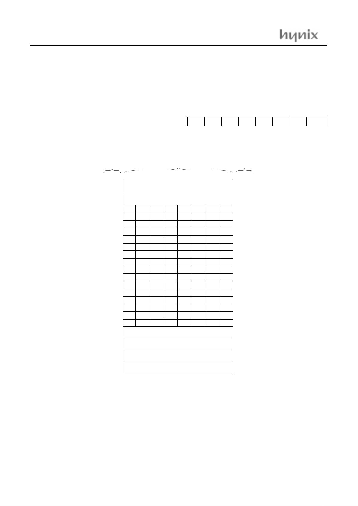
SFR
The SFRs can only be ad dressed directly in the address range
from 128 to 2 55. Tab le 8.2 gi ves an ov erview of the Spe cial F unction Regi sters spac e. Sixteen a ddress in th e SFRs space are both-
byte and bit-addre ssable. The bit-a ddressable SFRs are tho se
whose address ends in 0H and 8H. The bit addresses in this area
are 80H to FFH.
Table 8-2 SFR Memory Map
Note: * The register that can be bit-addressing.
F8
- HVGEN CPGEN VFH VFL HFH HFL
FF
F0
*B MDCON MDST VPH HPH VHPL
F7
E8
*EXCON - - -
EF
E0
*ACC-- ----
E7
D8
*S1CON S1STA S1DAT S1ADR0 S2CON S2STA S2DAT S2ADR
DF
D0
*PSW S1SDR1 RAMBUF DDCDAT DDCADR DDCCO N
D7
C8
*T2CON - RC2L RC2H - -
CF
C0
- -
C7
B8
*IP -
BF
B0
*P3 DPWMCON DPWM0 DPWM 1 - IPA -
B7
A8
*IE - PWM4 PWM5 PWM6 PWM7 WDTKEY
AF
A0
*P2 PWMCON PWM0 PWM1 PWM2 PWM3 WDTRST IEA
A7
98
--
9F
90
*P1 P1SFS P2SFS P3SFS ADAT ACON
97
88
*TCON TMOD TL0 TL1 TH0 TH1
8F
80
*P0 SP DPL DPH PCON
87
Page 24
HMS9 xC 7132 / HMS9xC7134
20 May.2001 ver1.1
8.4 List of SFRS
Register Description Address R/W
Initial V a lu e
76543210
P0 Port0 Register 80H R/W 11111111
SP Stack Point register 81H R/W 00000111
DPL Data Pointer(Low byte) Register 82H R/W 00000000
DPH Data Pointer(High byte) Register 83H R/W 00000000
PCON Power Control Register 87H R/W xx 000000
TCON Timer/Counter Control Register 88H R/W 00000000
TMOD Timer/Counter Mode Control Register 89H R/W 00000000
TL0 Timer/Counter0 Low byte Register 8AH R/W 00000000
TL1 Timer/Counter1 Low byte Register 8BH R/W 00000000
TH0 Timer/Count er0 High byte Register 8CH R/W 00000000
TH1 Timer/Count er1 High byte Register 8DH R/W 00000000
P1 Port1 Register 90H R/W 11111111
P1SFS Port1 Special Function Selection Register 91H R/W 00000000
P2SFS Port2 Special Function Selection Register 92H R/W 00000000
P3SFS Port3 Special Function Selection Register 93H R/W 00000000
ADAT ADC Data Register 96H R/W 00000000
ACON ADC Control Register 97H R/W xx 0 x0001
P2 Port2 Register 0A0H R/W 11111111
PWMCON PWM Control Register 0A1H R/W 00000000
PWM0 PWM0 Output Register 0A2H R/W 11111111
PWM1 PWM1 Output Register 0A3H R/W 11111111
PWM2 PWM2 Output Register 0A4H R/W 11111111
PWM3 PWM3 Output Register 0A5H R/W 11111111
PWM4 PWM4 Output Register 0AAH R/W 11111111
PWM5 PWM5 Output Register 0ABH R/W 11111111
PWM6 PWM6 Output Register 0ACH R/W 11111111
PWM7 PWM7 Output Register 0ADH R/W 11111111
WDTKEY Watchdog Key Register 0AEH R/W 00000000
WDTRST Watchdog Timer Reset Register 0A6H R/W 00000000
IEA Interrupt Enable Register 0A7H R/W 0 xxxxx00
IE Interrupt Enable Register 0A8H R/W 00000000
P3 Port3 Register 0B0H R/W 11111111
DPWMCON Dynamic PWM Control Register 0B1H R/W 0xxxxx00
DPWM0 Dynamic PWM0 Output Register 0B2H R/W 11111111
DPWM1 Dynamic PWM1 Output Register 0B3H R/W 11111111
IPA Interrupt Priority Register 0B6H R/W 0xxxxx00
IP Interrupt Priority Register 0B8H R/W x0000000
T2CON Timer2 Control Register 0C8H R/W 0xxxx0xx
RC2L Reload Low Register 0CAH R/W 00000000
RC2H Reload High Register 0CBH R/W 00000000
PSW Program Status Word Register 0D0H R/W 00000000
RAMBUF RAM Buffer I/O Interface Register 0D4H R/W xxxxxxxx
Page 25
HMS9xC7132 / HMS9xC7134
May.2001 ver1.1
21
DDCDAT Data Shift Register for DDC1 0D5H R/W 00000000
DDCADR DDC Address Pointer Register 0D6H R/W 00000000
DDCCON DDC Mode Status and DDC1 Control Register 0D7H R/W x 0 0 x 0000
S1CON Serial Control Register for DDC2 0D8H R/W 00000000
S1STA Serial Status Regist er for DDC2 0D9H R 0 x 0 0 xxxx
S1DAT Data Shift Register for DDC2 0DAH R/W 00000000
S1ADR0 Serial Address0 Register for DDC2 0DBH R/W 0000000x
S1ADR1 Serial Address1 Register for DDC2 0D3H R/W 0000000x
S2CON Serial Control Register 0DCH R/W 00000000
S2STA Serial Status Register 0DDH R 0x00xxxx
S2ADR Serial Address Register for I2C 0DFH R/W 0000000x
S2DAT Data Shift Register for I2C 0DEH R/W 00000000
ACC Accumulator 0E0H R/W 00000000
EXCON Extended Control Register 0E8H R/W xxxxxxx0
B B Register 0F0H R/W 00000000
MDCON Mode Indication Register 0F1H R/W 0 0 0 x x 0 0 0
MDST Mode Status Register 0F2H R x0000000
VPH Vertical scan period High byte Register 0F3H R/W 00000000
HPH Horizontal scan period High byte Register 0F4H R/W 00000000
VHPL V/H scan period High byte Register 0F5H R/W 00000000
HVGEN H/V pulse Control Register 0F9H R/W x 0 0 0 x 0 0 0
CPGEN Clamping pulse and Pattern Control register 0FAH R/W 00000x 00
VFH
Vertical free- running outp ut pulse period Hi gh byte
register
0FBH R/W 00100000
VFL
Vertical free-running output pulse period Low byte
register
0FCH R/W 00001010
HFH
Horizontal free-running output pulse per iod High
byte register
0FDH R/W 01100000
HFL
Horizontal free-running output pulse per iod Low
byte register
0FEH R/W 00x11111
Register Description Address R/W
Initial V a lu e
76543210
Page 26
HMS9 xC 7132 / HMS9xC7134
22 May.2001 ver1.1
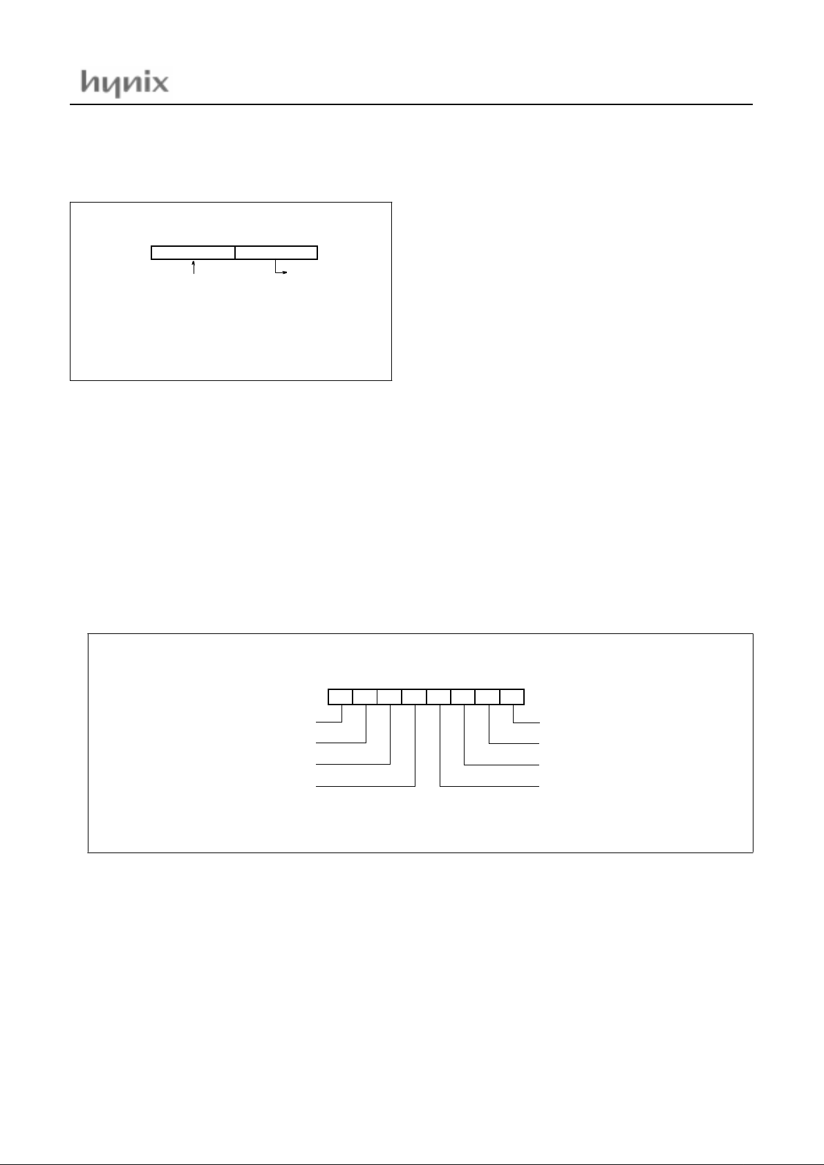
8.5 Addressing Mode
The address ing modes in HMS9xC7 132 instruct ion set are as fo llows
• Direct addressing
• Indirect addressing
• Register addressing
• Register-specific addressing
• Immediate constants addr essing
• Indexed addressing
Note that refer to “Chapter 22. Instruction Set” those addressing modes and related instructio ns.
(1) Direct addressing
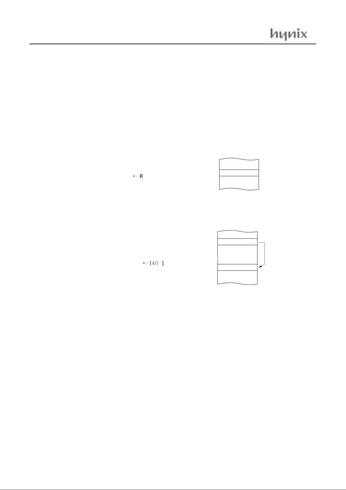
In a direct a ddr essi ng th e op erand is s pecif ie d by an 8-bi t a ddres s
field in the instruction. Only internal Data RAM and
SFRs(80~FFH RAM) can be directly addressed.
Example:
mov A, 3EH ; A RAM[3E]
(2) Indirect addressing
In indirect addressing the instruction specifies a register which
contains the address of the operand. Both internal and external
RAM can be indirectly addressed. The address register for 8-bit
addresses can be R0 or R1 of the selected register bank, or the
Stack Pointer. The address register for 16-bit addresses can only
be the 16-bit “data pointer” registe r, DPTR.
Example:
mov @R1, 40 H ;[R1]
H]
(3) Register addressing
The register banks, containing registers R0 through R7, can be
accessed by certain inst ructions which car ry a 3-bit register spec ificat ion with in the opco de of the ins truct ion. Inst ruct ions th at access the registers th is way are cod e efficient, since th is mode
eliminates an address byte. When t h e instr uction is execute d, one
of four banks is sel ected at e xecution t im e by the two bank select
bits in the PSW.
Example; mov PSW, #0001000B ; sele ct Bank0
mov A, #30H
mov R1, A
(4) Register-specific addressing
Some instructions are specific to a certain register. For example,
some instructions always operate on the Accumulator, or Data
Pointer, etc., so no address b yte is needed to point it . The opcode
itself does that.
→ A
04
PROG. MEMOR Y
3E
H
55
40
H
~
~
~
~
55
R1
PROG. MEMORY
Page 27
HMS9xC7132 / HMS9xC7134
May.2001 ver1.1
23
(5) Immediate constants addressing
The valu e of a constant can follow the opcode in Program mem ory.
Example; mov A, #100H.
(6)Indexed addressing
Only Progra m memor y ca n be acces se d wit h indexe d add res sing,
and it can only be read. This addressing mode is intended for
reading l ook-up tab les in Progra m memory . A 16-bi t base registe r
(either DPTR or PC) points to the base of the table, and the Accumulator is set up with the table entry number. The address of
the table entry in Program memory is formed by adding the Accumu la to r data to the bas e p oi nt er.
Example; movc A, @A+DPTR
1EAD
H
~
~
~
~
ACC DPTR
3A 1E73
PROG. MEMORY
Page 28

HMS9 xC 7132 / HMS9xC7134
24 May.2001 ver1.1
9. INTERRUPTS
There are in terrupt requests from 9 sources as follows.
• INT0 external interrupt
• INT1 external interrupt
•Timer0 interrupt
• Timer1 interrupt
• Timer2 interrupt
• DDC interrupt
• MD interrupt
• VSYNC interrupt
• I2C interrupt
9.1 Interrupt sources
INT0 external interrupt:
•The INT0 ca n be either level-active or transition-activ e depending on bi t IT0 in r egister TCON. The flag that actually gene rates
this interrupt is bit IE0 in TCON.
•
When an external interrupt is generated, the corresponding re-
quest flag is cleared by the hardware when the service routine is
vectore d to only if the interrupt wa s transiti on-activated.
• I
f the interrupt was level-activated then the interrupt request flag
remains set until the requested interrupt is actually generated.
Then it has to dea ctiv ate t he r equ est b efo re th e in terr up t se rvic e
routine is completed, or else another interrupt will be generated.
INT1 external interrupt:
•T
he INT1 can be ei ther level -active or transition-active dep ending on bit IT1 in register TCON. The flag that actually generates
this interrupt is bit IE1 in TCON.
•
When an external interrupt is generated, the corresponding re-
quest flag is clea re d by the hardw a re when the ser vice routine is
vectore d to only if the interrupt wa s transiti on-activated.
• If the in terr upt was l evel- activa ted the n the i nterrup t reque st fl ag
remains set until the requested interrupt is actually generated.
Then it has to dea ctiv ate t he r equ est b efo re th e in terr up t se rvic e
routine is completed, or else another interrupt will be generated.
MD interrupt:
•A MD interrupt is generated by the hardware mode detector in
case of mode change, horizontal or vertical.
• This flag has to be clear e d by the software.
VSYNC interrupt:
•The changing of the VSYNC level can generate an interrupt.
This depends on the setting that is programmed in the MDCONSFR. Via this regis ter it is possible to enable the edge of the
VSYNC-sig nal t hat sh ould g ene rat e the i nte rrupt . Both e dges ca n
be contro lled separately.
• The interrupt flag ha s to be cleared by the softwar e.
DDC interrupt:
•The DDC interr upt is gener ated ei ther by bit INTR in th e S1STA
register for DDC2B/DDC2AB/DDC2B+ protocol or by bit
DDC_int in the DDCCON register for DDC1 protocol or by bit
SWHINT bit in the DDCCON re gister when DDC protocol is
changed fr om D D C 1 to D D C 2.
• Flags except the INTR have to be cl eared by the software . INTR
flag is cleared by hardware.
I2C interrupt:
•The interrupt of the second I2C is generated by bit INTR in the
register S2STA.
• This flag is cleared by hardware.
Page 29

HMS9xC7132 / HMS9xC7134
May.2001 ver1.1
25
Timer0 and Timer1 interrupt:
•Timer0 and Timer1 interrupts are generated by TF0 and TF1
which are set by an overflow of their respective Timer/Counter
registe rs(except for Timer0 in mode3).
•These flags are cleared by the inter nal hardware.
Timer2 interrupt:
•Timer2 i nterrupt is gen erate d by TF2 whic h is set by an over flow
of Timer2.
• This flag has to be clear e d by the software.
All of the bits that generate interrupts can be set or cleared by software, with the same result as though it had been set or
cleared by hardware. That is, interrupts can be generated or pending interrupts can be cancelled in software.
Figure 9-1 Inter rupt system
INT0
MD
Timer0
I2C
INT1
DDC
Timer1
VSYNC
Not
used
Timer2
High
Low
Interrupt Pollin g Sequen ce
Interrupt
Sources
IE / IEA IP / IPA Priority
Global
Enable
Page 30

HMS9 xC 7132 / HMS9xC7134
26 May.2001 ver1.1
9.2 Interrupt Enable structure
Each interrupt source can be individually enabled or disabled by
setting or clearing a bit in the interrupt enable special function
register IE and IEA . All i n terrupt source can also be globally disabled by cl earing bit EA in I E.
Table 9-1 Interrupt Enabl e Regist er(IE: 0A8H) RESET VALUE:00000000B
Table 9-2 Description of the IE bits
Table 9-3 Interrupt Enable Register(IEA: 0A7H) RESET VALUE:0xxxxx00B
Table 9-4 Description of Enable Register(IEA: 0A7H)
76543220
EA EVSYNC ET2 ES ET1 EX1 ET0 EX0
BIT SYMBOL FUNCTION
7EA
Disable all interrupts.
0 : no interrupt will be acknowledged
1 : each interrupt source is individually enabled or disabled by setting or clear
ing its enable bit
6 EVSYNC
Enable Vsync interrupt
5ET2
Enable timer2 interrupt
4ES
Not used
3ET1
Enable timer1 interrupt
2 EX1
Enable external interrupt (INT1)
1ET0
Enable timer0 interrupt
0 EX0
Enable external interrupt (INT0)
76543220
EDDC-----EI2CEMD
BIT SYMBOL FUNCTION
7EDDC
Enable DDC interrupt
6 EX6
Not used
5 EX5
Not used
4 EX4
Not used
3 EX3
Not used
2 EX2
Not used
1EI2C
Enable I2C interrupt
0EMD
Enable MD interrupt
Page 31

HMS9xC7132 / HMS9xC7134
May.2001 ver1.1
27
9.3 Interrupt Priority structure
Each interrupt source ca n be assigned one of tw o priority levels.
Inte rr up t prior ity l evels a re d ef ined by t h e interr up t priority sp e-
cial function register IP and IPA.
“0” - low priority
“1” - high priority
A low priority interrupt may be interrupted by a high priority in-
terrup t level int errupt. A high priority interr upt routine cannot be
interrupted by any ot her inter rupt source . If two interrupts of different priority occur simultaneously, the high priority level request is serviced. If requests of the same priority are received
simultaneously, an internal polling sequence determines which
request is se rvic ed. Thus , within eac h prior ity leve l, there is a second priority structure determined by the polling sequence. This
second pri ority structure is shown i n Table 9.5.
Table 9-5 Priori ty levels
Note
• The “Priority with in level ” stru cture i s only used to resol ve
simultaneous requests of the same prior ity level.
• The MD interrup t needs a hi gher pr iori ty then ALL the oth er interrupts. This is to avoid that a mo de change will not be
serviced in ti me and that the setting of the S-curv e is not updated in time. When the S-curve set tings are not updated in
time (after a mode chan ge) the monitor may be damaged.
Table 9-6 Interrupt Priority Register(IP: 0B8H) RESET VALUE: x0000000B
Table 9-7 Description of the IP bits
SOURCE PRIORITY WITHIN LEVEL
INT0
MD
Timer0
I2C
INT1
DDC
Timer1
VSYNC
Timer2
1(highest)
9(lowest)
76543220
- PVSYNC PT2 PS PT1 PX1 PT0 PX0
BIT SYMBOL FUNCTION
7-
Reserved
6 PVSYNC
Vsync interrupt priority level
5PT2
Timer2 interrupt priority level
4PS
Not used
3PT1
Timer1 interrupt priority level
2 PX1
External interrupt (INT1) priority level
1PT0
Timer0 interrupt priority level
0 PX0
External interrupt (INT0) priority level
Page 32

HMS9 xC 7132 / HMS9xC7134
28 May.2001 ver1.1
Table 9-8 Interrupt Priority Register(IPA: 0B6H) RESET VALUE: 0xxxxx00B
Table 9-9 Description of the IPA bits
76543220
PDDC-----PI2CPMD
BIT SYMBOL FUNCTION
7PDDC
DDC interrupt priority level
6 PX6
Not used
5 PX5
Not used
4 PX4
Not used
3 PX3
Not used
2 PX2
Not used
1PI2C
I2C i n terrup t p r io rity le vel
0PMD
MD interrupt priority level
Page 33

HMS9xC7132 / HMS9xC7134
May.2001 ver1.1
29
9.4 How Interrupt are handled
The interrupt flags are sampled at S5P2 of every machine cycle.
The samples are pol le d dur ing fo ll owi ng mac hin e cycl e. If one o f
the flag s was i n a s et c ondi tion a t S5P2 of t he prec edi ng cycle , the
polling cycle w ill fi nd it an d the int er rupt syst em w ill gene ra te an
LCALL to the app ropriate service routine, provided this H/ W
generated LCALL is not blocked by any of the following conditions :
• An interrupt of equal priority or higher priority level is already in progress.
• The current machine cycle is not the final cycle in the execution of the instruction in progress.
• The instruction in progress is RETI or any access to the
interrupt prior ity or interrupt enable registers.
The polling cycle is repeated with each machine cycle, and the
values pol led are the values that were present at S5P2 of the pre vious machi ne cycl e. Note that if an in terr upt fl ag is acti ve but be ing res ponded t o for o ne of the a bove me nt ioned co ndi tions , if th e
flag is still inactive when the blocking condition is removed, the
denied interrupt will not be serviced. In other words, the fact that
the inte rrupt fla g wa s on ce ac tive but no t s erviced is not reme m bered. Eve ry polling cycle is new.
The processor acknowledges an interrupt request by executing a
hardware generated LCALL to the appropriate service routine.
The hardware generated LCALL pushes the contents of the Program Counter on to the stack (but it does not save the PSW) and
reloads the PC with an address that depends on the source of the
interrupt being vect ored to as shown in Table 9-10.
Execution proceeds from that location until the RETI instruction
is encountered. The RETI instruction informs the processor that
the interrupt routine is no longer in progress, then pops the top
two bytes from the stack and reloads the Program Counter. Execution of t he in te rrupt ed pr ogram con ti nue s from whe re i t le ft o ff .
Note that a simple RET instruction would also return execution
to the interrupted program, but it would have left the interrupt
control system thinking an interrupt was still in progress, making
future interrupts impossible.
Table 9-10 Vector addresses
SOURCE VECTOR ADDRESS
INT0 0003H
MD 004BH
Timer0 000BH
I2C 0043H
INT1 0013H
DDC 003BH
Timer1 001BH
VSYNC 0033H
Timer2 002BH
Page 34

HMS9 xC 7132 / HMS9xC7134
30 May.2001 ver1.1
10. POWER-SAVING MODE
Two software selectable modes of reduced power consumption are implemented.
• Idle mode
• Power-down mode
The following functions are switche d off when the microcontroller enters the Idle mode.
• CPU (halted)
• I2C interface (halted)
• PWM0 to PWM7 and DPWM0 to DPWM2 (reset, output = High)
• 8-bit ADC (aborted if conversion in progress)
The followi ng functions rem ain active during Idle mode.
These funct ions may gene rate an interr upt or reset and thus termin ate the Idle mode.
• Timer0, Timer1 and Timer2
• Watchdog timer
• DDC interface
• External interrupt
• Mode detection
In Power-down mode, the system clock is halted. Both the oscillator will be stopped after setting the bit PD in PCON.
10.1 Power control register
The modes Idle and Power-down are activated by software via the PCON register.
Table 10-1 Power control Register( PCON:87H) RESET VALUE:xx000000B
Table 10-2 Description of t he PCON bits
76543220
- - LVREN LVRLS GF1 GF0 PD IDL
BIT SYMBOL FUNCTION
7 to 6 -
Not used
5 LVREN
Enable low voltage reset
4LVRLS
Select low VDD level ; 3.7V or 3.5V
3GF1
General purpose flag bit
2GF0
General purpose flag bit
1PD
Activate Power-down mode
0IDL
Activate Idle mode
Page 35

HMS9xC7132 / HMS9xC7134
May.2001 ver1.1
31
Table 10-3 External Pin Sta tus Duri ng Idle and Power-down modes
10.2 Idle mode
The ins tr ucti on th at set s PC ON.0 is the la st instr uct ion ex ecu t ed
in the nor mal ope rati ng mo de b ef ore id le m ode is act i vated. Onc e
in the id le mode , th e CP U s tatus i s pr eserv ed in i ts e nti r et y : Stac k
pointer, Program counter, Program status word, Accumulator,
RAM and All othe r regist ers mainta in thei r data duri ng idle
mode.
There are th ree ways to term inate the id le mode.
• Activation of any enabled interrupt X0, T0, X1, T1 etc. will
cause PCON.0 to be cleared by hardware termina ti ng Idle
mode. The interrupt is serviced, and following return from
interrupt instruction RETI, the next instruction to be executed will be the one which follows the inst ruction that wrote a
logic 1 to PCON.0.
• External hardware reset : the hardware reset is required
to be activ e fo r two mac hi ne cycl e t o comp lete t he res et operation.
• Internal wat chdog reset : the microcontroller restarts aft er
3 machine cycles in all cases.
10.3 Power-down mode
The instruction that sets PCON.1 is the last executed prior to going into the Power-down mode. Once in Power-down mode, the
oscillator is stopped. The contents of the on-chip RAM and the
Special Function Register are preserved.
The power- dow n m ode can be termi nated by an external RESET
in the sam e way a s i n the 80C 51 ( but SFRs ar e clear ed due to RESET).
MODE MEMORY PORT0-3 SYNC PWM I2C DDC - Idle Intenal Data on High High-Z on - Power-down Intenal Data High High High-Z High-Z - -
Page 36

HMS9 xC 7132 / HMS9xC7134
32 May.2001 ver1.1
11. I/O PORTS
The HMS9xC7132 has four 8-bit ports (Port0, Port1, Port2 and
Port3). Port0 - Port3 are the same as in the 80C51, with the exception of the addi tional functions of Port1, Port2 and Port 3. All
ports are bidirectional and Pins of which the alternative function
is not used may be used as normal bidirectional I/Os except
Port3.2, Port3.3 and Port3.5(These Pins can be only used as the
output).
The use of Port1- Port3 pins as alternative functions are carried
out automatically by the HMS9xC7132 provided the associated
SFR bi t is set HIGH .P o rt0 is the ty p e o f op en-dra in I/O . Por t0.6
and Port0.7 have the capability to drive LED.
Fig. 11.1 show s the port stru cture.
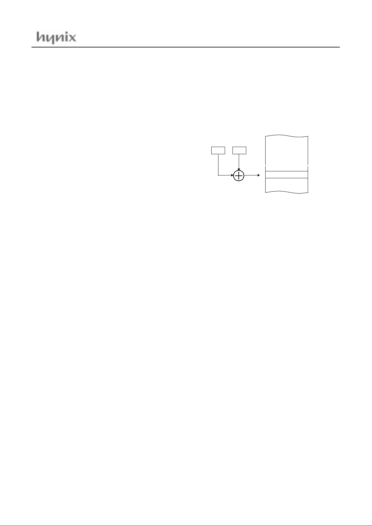
Figure 11-1 Standard out put with the open-drain port
The alternative function for Port1, Port2 and Port3 can be described as follows.
• Port 0 : No alternative function.
• Port 1 : P1.0 is combined with the SCL1 interface line(open-drain)
P1.1 is combined with the SDA1 interface line (open-drain)
P1.2 is combined with the ACH0 interface line (high-z)
P1.3 is combined with the ACH1 interface line (high-z)
P1.4 is combined with the ACH2 interface line (high-z)
P1.5 is combined with the ACH3 interface line (high-z)
P1.6 is combined with the SCL2 interface line (open-drain)
P1.7 is combined with the SDA2 interface line (open-drain)
• Port 2 : P2.0 is combined with the dyn amic PW M 0 int erface line(open-drain or push-pull)
P2.1 is combined with the dynamic PWM1 interface line (open-drain or push-pull)
P2.2 is combined with the static PWM0 interface line (open-drain or push-pull)
P2.3 is combined with the static PWM1 interface line (open-drain or push-pull)
P2.4 is combined with the static PWM2 interface line (open-drain or push-pull)
P2.5 is combined with the static PWM3 interface line (open-drain or push-pull)
P2.6 is combined with the static PWM4 interface line (open-drain or push-pull)
P2.7 is combined with the static PWM5 interface line (open-drain or push-pull)
• Port 3 : P3.0 has not alternative function.
P3.1 has not alternative function.
P3.2 is combined with the HSYNCout interface line (push-pull)
P3.3 is combined with the VSYNCout interface line (push-pull)
P3.4 is combined with the PWM6 interface line (open-drain or push-pull)
P3.5 is combined with the CLAMP or PWM7 interface line (push-pull)
P3.6 is combined with the PATOUT interface line (push-pull)
P3.7 is combined with the SOG interface line (pull-up)
I/O PIN
Port Data
Input Data
Specia l Da ta / Gn d
Specia l Function Selec t
0
1
Enable / Data
Page 37

HMS9xC7132 / HMS9xC7134
May.2001 ver1.1
33
11.1 Pin function selection
Special function selection Registers(PxSFS)
Several SFR(P1SFS/P2SFS/P3S FS)s are used to select the port-f unction or the alternative function of the ext ernal pin.
• P1SFS(Port1 special function selection register)
Table 11-1 P1SFS bits(91H)
Table 11-2 Descript ion of the P1SFS bit s
76543220
P1SFS7 P1SFS6 P1SFS5 P1SFS4 P1SFS3 P1SFS2 P1SFS1 P1SFS0
BIT SYMBOL FUNCTION RESET
7P1SFS7
The selection of the pin function.
0 : pin 9 has P1.7 function.
1 : pin 9 has SDA2 function.
0
6P1SFS6
The selection of the pin function.
0 : pin 10 has P1.6 function.
1 : pin 10 has SCL2 out function.
0
5P1SFS5
The selection of the pin function.
0 : pin 20 has P1.5 function.
1 : pin 20 has ACH3 out function.
0
4P1SFS4
The selection of the pin function.
0 : pin 21 has P1.4 function.
1 : pin 21 has ACH2 out function.
0
3P1SFS3
The selection of the pin function.
0 : pin 22 has P1.3 function.
1 : pin 22 has ACH1 out function.
0
2P1SFS2
The selection of the pin function.
0 : pin 23 has P1.2 function.
1 : pin 23 has ACH0 out function.
0
1P1SFS1
The selection of the pin function.
0 : pin 24 has P1.1 function.
1 : pin 24 has SDA1 out function.
0
0P1SFS0
The selection of the pin function.
0 : pin 25 has P1.0 function.
1 : pin 25 has SCL1 out function.
0
Page 38

HMS9 xC 7132 / HMS9xC7134
34 May.2001 ver1.1
• P2SFS(Port2 special function selection register)
Table 11-4 Descript ion of the P2SFS bit s
76543220
P2SFS7 P2SFS6 P2SFS5 P2SFS4 P2SFS3 P2SFS2 P2SFS1 P2SFS0
Table 11-3 P2SFS bits(92H)
BIT SYMBOL FUNCTION RESET
7P2SFS7
The selection of the pin function.
0 : pin 34 has P2.7 function.
1 : pin 34 has PWM5 function.
0
6P2SFS6
The selection of the pin function.
0 : pin 35 has P2.6 function.
1 : pin 35 has PWM4 out function.
0
5P2SFS5
The selection of the pin function.
0 : pin 36 has P2.5 function.
1 : pin 36 has PWM3 out function.
0
4P2SFS4
The selection of the pin function.
0 : pin 37 has P2.4 function.
1 : pin 37 has PWM2 out function.
0
3P2SFS3
The selection of the pin function.
0 : pin 38 has P2.3 function.
1 : pin 38 has PWM1 out function.
0
2P2SFS2
The selection of the pin function.
0 : pin 1 has P2.2 function.
1 : pin 1 has PWM0 out function.
0
1P2SFS1
The selection of the pin function.
0 : pin 2 has P2.1 function.
1 : pin 2 has DPWM1 out function.
0
0P2SFS0
The selection of the pin function.
0 : pin 3 has P2.0 function.
1 : pin 3 has DPWM0 out function.
0
Page 39

HMS9xC7132 / HMS9xC7134
May.2001 ver1.1
35
• P3SFS(Port3 special function selection register)
Table 11-5 P3SFS bits(93H)
Table 11-6 Descript ion of the P3SFS bit s
76543220
P3SFS7 P3SFS6 P3SFS5 P3SFS4 P3SFS3 P3SFS2 P3SFS1 P3SFS0
BIT SYMBOL FUNCTION RESET
7P3SFS7
The selection of the pin function.
0 : pin 28 has P3.7 function.
1 : pin 28 has SOG input function.
0
6P3SFS6
The selection of the pin function.
0 : pin 29 has P3.6 function.
1 : pin 29 has PATOUT out function.
0
5P3SFS5
The selection of the pin function.
0 : pin 30 has P3.5 function.
1 : pin 30 has CLAMP or PWM7 out function.
0
4P3SFS4
The selection of the pin function.
0 : pin 31 has P3.4 function.
1 : pin 31 has PWM6 out function.
0
3P3SFS3
The selection of the pin function.
0 : pin 32 has P3.3 function.
1 : pin 32 has VSYNCout function.
0
2P3SFS2
The selection of the pin function.
0 : pin 33 has P3.2 function.
1 : pin 33 has VSYNCout function.
0
1P3SFS1
The selection of the pin function.
reserved
0
0P3SFS0
The selection of the pin function.
reserved
0
Page 40

HMS9 xC 7132 / HMS9xC7134
36 May.2001 ver1.1
12. OSCIALLTOR
The oscillat or ci rcuit of the HMS9 xC7132 is a si ngle s tage inver ting amplifier in a Pierce oscillator configuration. The circuitry
between XTAL 1 and XTAL2 is basic ally an in verte r biased t o the
transfer point. Either a crystal or ceramic resonator can be used as
the feedback element to complete the oscillator circuit. Both are
operated in parallel resonance.
XTAL1 is the high gain amplifier input, and XTAL2 is the output. To dri ve the HM S9xC7132 externally , XTAL1 is driven
from an external sour ce and XTAL2 left o pen-circui t.
Figure 12-1 Oscil lat or configuration
Main clock
Minimum instruction cycle time
(ex:NOP ; f
ex
12clock is needed)
12MHz 1uS
XTAL1
XTAL2
XTAL1
XTAL2
External clock
10 ~ 16MHz
reset
Vdd
reset
Vdd
4.2V
ideal standard; R=10K
C=10uF (Recommanded)
reset IC
R
C
Page 41

HMS9xC7132 / HMS9xC7134
May.2001 ver1.1
37
13. RESET
There are three ways to invoke a reset and initialize the
HMS9xC7132.
Via the exter nal RESET pin
Via the Watchdog Timer overflow
Via low VDD voltage reset
Each reset source will cause an internal reset signal active. The
CPU responds by exe cuti ng an inter nal re set and put s th e inte rna l
registers in a defined state.
Figure 13-1 The reset mechanism
13.1 External reset
The reset pin RESET is connected to a Schmitt trigger for noise
reduction. A reset is accomplished by holding the RESET pin
LOW for at least 2 machine cycles (24 system clock), while the
oscillator is running.
An automatic reset can be obtained by switching on VDD, if the
RESET pin is connected to GND via a capacitor and to the VDD
via resistor. The capacitor should be at least 10uF.
The increase of the RESET pin v oltage dep ends on the capacitor.
The voltage must remain below the higher threshold for at minimum the oscillator start-up time plus 2 machine cycles.
13.2 Watchdog timer overflow
The length of the output pulse from the WDT i s over 2048 machine cycles. In c hapter 14, the watchdog ti mer is described in more de tail .
13.3 Low VDD voltage reset
When VDD is below 3.7V, the built-in low voltage detector generates an internal reset signals. The reset signal will be LOW during 2ms
@12MHz afte r th e vo ltage is hi g her than 3. 7V .
WDT
LVR
S Q
R
2.0m s
Timer
RESET
RSTOUT
CPU&
PERI.
NC
Page 42

HMS9 xC 7132 / HMS9xC7134
38 May.2001 ver1.1
14. WATCHDOG TIMER
The hardware watchdog timer (WDT) resets the HMS9xC7132
when it over flow s. Th e WDT is i nt end ed as a re cov er y met hod in
situa tio ns w her e the C PU m ay be s ubj ec ted to a s oft war e u pse t.
To prevent a system reset the timer must be reloaded in time by
the appli cati on sof tw are. I f th e pro ces so r suffe rs a har dwar e/sof t ware m a lf un ction, t he s of tw a re w ill fail to re lo a d the time r. T h is
failure will result in a reset upon overflow thus preventing the
processo r running out of c ontrol.
In the idle mo de the watch dog timer and res et circui try rem ain active. The WDT consists of a 19-bit counter, the watchdog timer
reset(WDTRST) S FR and watchdog key reg ister(WDTKEY).Since the WDT i s automatically enabled while the processor is run ning. the use r on ly need s t o be c once rn ed with ser vi ci ng
it.The 19-bi t cou nt er overf l ows when it reach es 52 4288 (3F FFH).
The WDT increments once every machine cycle.
This means the user must reset the WDT at least every 524288
machine cycles (524ms @12MHz). To reset the WDT the usermust write 01EH and then 0E1H to W DTRST. WDTRS T is a
write only register. The WDT count cannot be read or writt en.
The watchdog timer is controlled by the watchdog key register,
WDTKEY. Only pattern 01010101(=55H), disables the watchdog timer. The rest of pattern combinations will keep the watchdog timer enabled. This security key will prevent the watchdog
timer from being terminated abnormally when the function of the
watchdog t im er is needed.
In Idle mode, the oscillator continues to run. To prevent the WDT
from res et ting th e pr ocess or whi le in Idle , th e u ser s houl d a lwa ys
set up a timer that will periodically exit Idle, service the WDT,
and re-enter Idle mode.
Table 14-1 Watchdog timer key register (WDTKEY : 0AEH) RESET VALUE:00000000B
Table 14-2 Description of t he WDTKEY bi ts
Table 14-3 Watchdog timer clear register (WDTRST : 0A6H) RESET VALUE:00000000B
Table 14-4 Description of t he WDTRST bi ts
Example Program; Watch Dog Timer
Reset & WDT_refresh Part
Reset:
clr EA
mov PSW, #00
mov SP, #STACK_DATA;
mov WDTKEY, #55h ;
Watchdog stop
WDT_refresh:
mov WDTRST, #1Eh ;
Watchdo g timer reset
mov WDTRST, #0E1h ;
Watchdog timer reset
mov WDTKEY, #0F0h ;
Watchdog start
ret
76543220
WDTKEY7 WDTKEY6 WDTKEY5 WDTKEY4 WDTKEY3 WDTKEY2 WDTKEY1 WDTKEY0
BIT SYMBOL FUNCTION
7 to 0
WDTKEY7
to
WDTKEY0
Enable or disable watchdog timer.
01010101(=55H) : di sable watchdog timer.
others : enable watchdog timer.
76543220
WDTRST7 WDTRST6 WDTRST5 WDTRST4 WDTRST3 WDTRST2 WDTRST1 WDTRST0
BIT SYMBOL FUNCTION
7 to 0
WDTKEY7
to
WDTKEY0
Enable or disable watchdog timer.
01010101(=55H) : di sable watchdog timer.
others : enable watchdog timer.
Page 43

HMS9xC7132 / HMS9xC7134
May.2001 ver1.1
39
15. TIMER
HMS9xC7132 has two 16-bit timers/counters (Timer0, Timer1) to be placed in 80C51 core and one 16-bit auto-reload timer(Timer2) for
dynamic PWM.
15.1 Timer0 and Timer1
The external input pin that the Timer/Counter0 and Timer/
Counter1 in 80C5 1 cor e ha ve is el imi nat ed . In the ti mer functi on,
timer register is incremented e very machine cycle. Thus, you can
think of it as c ounti ng mach in ecy cles. S ince a machi ne c ycle con sists of 12 oscillator periods, the count rate is 1/12 of the oscilla-
tor frequency.
Timer 0, Timer 1 have four operating modes. These modes is se-
lected by bit-pairs(M1, M0) in TMOD.
Table 15-1 Timer Mode Control register(TMOD) RESET VALUE:00000000B
Table 15-2 Description of the TMOD bits
76543220
GATE C/T M1 M0 GATE C/T M1 M0
BIT SYMBOL FUNCTION
7,3 GATE
Gating control when set. Timer “x” is enabled only while “INTx” pin is high
and “TRx” control bit is set. When cleared Timer”x” is enabled whenever
“TRx”control bit is set.
6,2 C/T
Timer or Counter selector
0 : Timer
1 : Counter, not supported.
7 to 0
M1, M0
0, 0
0, 1
1, 0
1, 1
Operating modes
8-bit Timer °THx” with “TLx” as 5-bit prescaler
16-bit Timer ”THx” and “TLx” are cascaded : there is no pr escaler
8-bit auto-reload Timer “THx” holds a value which is to be reloaded into
“TLx” each time it overflows.
Timer0 : TL0 is an 8-bit Timer controlled by the standard
Timer 0 control bit.
: TH0 is an 8-bit timer only controlled by Timer 1 control bit.
Timer1 : Timer 1 stopped.
Page 44

HMS9 xC 7132 / HMS9xC7134
40 May.2001 ver1.1
Table 15-3 Timer Control register(TCON) RESET VALUE:00000000B
Table 15-4 Description of t he TCON bits
15.2 TIMER2
Timer2 is a 16-bit auto-reload timer. The 16-bit capture mode,
baud rate generation mode and an event counter func tion that the
Timer/C ounte r2 in 8 0C52 co re has are eliminat ed. Sin ce t he
clock of this timer come s from the system oscillat or, Timer2 can
be used to count a time period more accurately comparing with
Timer0 and Timer1, but the longest period is limited as 65536 x
(tOSC/2).
The interval between interrupt =
65536 x (2 x tOSC) - (RC2H x 256 + RC2L) x (2 x tOSC)
The maximum i nterrupt per iod =
65536 x (2 x tOSC)
Table 15-5 Timer2 control register (T2CON : 0C8H) RESET VALUE:0xxxx0xxB
Table 15-6 Description of t he TCON bits
76543220
TF1 TR1 TF0 TR0 IE1 IT1 IE0 IT0
BIT SYMBOL FUNCTION
7 TF1
Timer1 overflow flag . Set by hardwar e on Timer oveflow.
Cleared by hardware when processor vectors to interrupt routine.
6 TR1 Timer1 run control bit . Set/cleared by software to turn Ti me r on/ off .
5 TF0
Timer0 overflow flag . Set by hardwar e on Timer oveflow.
Cleared by hardware when processor vectors to interrupt routine.
4 TR0 Timer0 run control bit . Set/cleared by software to turn Ti me r on/ off .
3IE1
Interrupt1 edge flag. Set by hardware when external interrupt edge detected.
Cleared when interrupt processed.
2IT1
Interrupt1 type control bit. Set/cleared by software to specified falling
edge/low level tri ggered external interr upts.
1IE0
I
nterrupt0 edge flag. Set by hardware when external int errupt edge detected.
Cleared when interrupt processed.
0IT0
Interrupt0 type control bit. Set/cleared by software to specified falling
edge/low level tri ggered external interr upts.
76543220
TF2----TR2--
BIT SYMBOL FUNCTION
7 TF2
Timer2 overflow flag . Set by hardwar e on Timer overflow.
Must be cleared by software.
6 to 3 - Reserved
2 TR2 Timer2 run cont rol bit. set/clear ed by software to turn Timer on/off.
1 to 0 TR0 Reserved
Page 45

HMS9xC7132 / HMS9xC7134
May.2001 ver1.1
41
Table 15-7 Reload/Captu re high register (RC2H : 0CBH) RESET VALUE:00000000B
Table 15-8 Reload/Capture low regis ter (RC2L : OCAH) RESET VALUE:00000000B
Example Program; Timer
Initial & Timer1 Interrupt part
initial:
; mov IP, #00h; Interrupt Priority
mov PCON, #00;
mov TCON, #01010000B;
T1, T0 enable
mov TMOD, #00010001B ;
16 bit timer set
mov IE, #11001000B; Global En(7) , Vsync( 6), Tim er1(3)
T1_Isr:
push PSW; PSW
push DPH; DPTR
push DPL;
push ACC; A
push 00h; R0
push 01h; R1
push 02h; R2
mov TH1, #0F0h;
F060h to Generate 4mSec
mov TL1, #60h;
76543220
RC2H7 RC2H6 RC2H5 RC2H4 RC2H3 RC2H2 RC2H1 RC2H0
BIT SYMBOL FUNCTION
7 to 0
RC2H7
to
RC2H0
Reload low register bit7 to bit0
76543220
RC2L7 RC 2L6 RC2L5 RC2L4 RC2L3 RC2L2 RC2L1 RC2L0
BIT SYMBOL FUNCTION
7 to 0
RC2L7
to
RC2L0
Reload low register bit7 to bit0
Page 46

HMS9 xC 7132 / HMS9xC7134
42 May.2001 ver1.1
16. DDC INTERFACE
The monitor typically includes a number of user controls to set
picture size, position, color balance, brightness and contrast.Furthermore, to optimize some internal setting for different display
modes, the timing characteristics should be acquired by the control side. In these days, it is getting popular for these controls to
go to PC host. Therefore the communication between monitor
and host becomes issue.D DC1, DDC2B, DDC2B+, and
DDC2AB(ACCESS.bus) emerge as a standa rd for monitor inter-
face. A t ransm itt er cl ocke d by incom ing V SYNC is ded ic ated f or
DDC1 operation. An I2C interface hardware logic forms the kernel of DDC2B, DDC2B+, and DDC2AB . An address pointer,
with p ost in cremen t capab ility is emplo yed to s erve DD C1,
DDC2B,DDC2B+ and DDC2AB modes.
The concept ual block diagram is illust rated in Fig. 16.1
Figure 16-1 DDC Interface bl ock diagram
DDC2B/DDC2AB
DDC2B+ Interface
S1ADR1
S1DAT
S1CON
S1STA
SDA1
SCL1
DDCCON
VSYNC
IN
INTR (From S 1 S T A )
INT
DDCADR
DDCDAT
X
EX_
DATSWENB
X
DDC1
INT
DDC1ENSWH
INT
M0
Initialization synchronization
DDC 1 tr an s m it ter
DDC1 Hold Register
Bus Clock Generator
Shift R eg ister
Monitor Address
Arbitrat ion Logic
DDC1/DDC2
Detection
RAMBUF
RAM
Buffer
Address Pointer
Internal B us
S1ADR0
7
10
Monitor Address
Page 47

HMS9xC7132 / HMS9xC7134
May.2001 ver1.1
43
16.1 The Special Function register for DDC Interface.
Eight SFR : S1CON, S1STA, S1DAT, S1ADR, RAMBUF, DDCCON, DDCADR, DDCDAT.
S1CON, S1STA, S1D A T , S1ADR are just the copies of the corresponding registers in general I2C-bus interface.
Table 16-1 DDC mode status and DDC1 control register (DDCCON : 0D7H) RESET VALUE:x00x0000B
Table 16-2 Description of the DDCCON bits
76543220
- EX_DAT SWENB - DDCINT DDC1EN SWHINT M0
BIT SYMBOL FUNCTION
7- Reserved
6
EX_DAT
(R/W)
This bit defines the size of the EDID data. It is related to the function of the post increment of the
address pointer, DDCADR. When the upper limit is reached, the DDCADR will wrap around to
00H.
If EX_DAT is
1: The data size is 256 byte.
0: The data size is 128 byte(T he addressing range f or the EDID data buf fer is mapped from 0 t o
127 ; the rest, 128 to 255 , can still be used by the system).
5
SWENB
(R/W)
This bit indicates if the software/CPU is needed to take care of the operation of DDC1 protocol.
If SWENB is
1 : In DDC1 protocol, CPU is interrupted during the period of the 9th transmitting bit so that the
S/W service rout ine can update the hold register of transmitt er by moving new data from appro priate area(i t is no t necessa ry to be the RAM buf f er which is pointed by DDCADR) to the re gi ster
DDCDAT. This transmitting must be done within 40us.
0 : The hold register of the tran smitte r will be aut omatical ly updat ed from th e RAM buffe r without
the interventi on of CPU.
4- Reserved
3
DDC1INT
(R/W)
Interrupt Request Bit. This bit is only valid in DDC1 pr otocol while S/W handling is enabled. This
bit is set by H/W and should be cleared by S/W in interrupt service routine.
1 : Interrupt request is pending.
0 : No interrupt req u e s t
2
DDC1EN
(R/W)
DDC1 enable control bit. If DDC1EN is
1 : DDC1 is enabled.
0 : DDC1 is disabled ; The activity on VSYNC is ignored.
1
SWHINT
(R/W)
Interrupt Request Bit. This bit is set by H/W when DDC interface switches from DDC1 to DDC2
(i.e. The voltage transient from high to low is observed on SCL1 pin) . Thi s bit should be cleared
by S/W in interrupt service routine.
1 : Interrupt request is pending.
0 : No interrupt req u e s t
0
M0
(R/W)
DDC mode indication bit . Thi s bi t will be set by H/W when the voltage tr ansient from high to low
is observed on SCL1 pin. Once mode changes int o DDC2 mode, the mode is reserved until power is off.
0: DDC1 is set.
1: DDC2 is set.
Page 48

HMS9 xC 7132 / HMS9xC7134
44 May.2001 ver1.1
DDC1 DATA register for transmission (
DDCDAT
: 0D5H)
• 8bit read and write register.
• Indicates DATA BYTE to be transmitted in DDC1 protocol.
Address pointer for DDC interface (
DDCADR
: 0D6H)
• 8bit read and write register.
• Address pointer with the capab il ity of the post increment. After each acc ess to RAMBUF register(either by
software or by hardware DDC1 interface), the content
of this register will be increased by one. It’s available-
both in DDC1, DDC2 (DDC2B, DDC2B+, and DDC2AB)
and system operation.
Host type detection
The detection procedure conforms to the sequences proposed by
VESA Monitor Display Data Channel(DDC) specification.The
monitor needs to determine the type of host system:
• DDC1 or OLD type host.
• DDC2B host (Host is master, monitor is always slav e)
• DDC2B+/DDC2AB(ACCESS.bus) host.
Page 49

HMS9xC7132 / HMS9xC7134
May.2001 ver1.1
45
The monitor where HMS9xC7132 resides is always both DDC1
and DDC2 capable with DDC2 having the higher priority. Thedisplay s hall s ta rt tr ans mit ti ng DDC1 sig nal s whe nev er it is po wered on and the verti cal sync sign al is appli ed to it from the
hostfor the first time. The display shall switch to DDC2 within 3
system clocks as soon as it sees a high to low transition on the
clockline(SCL), indicating that there are DDC2 devices connected to the bus. Under that condition, the mode flag, M0 will be
changed from the default setting 0, to 1. Accordingly, the interrupt will be invoked by sett ing flag, SWHIN T as high.
Fig. 16.2 i llu str at es the con cep t and i nt er actio n be twe en t he mo nitor and the host. After power on, the DDC1EN bit is set by S/W
to act as a DDC1 device. Therefore, the mode flag, M0, is set as
0. Following VSYNC as clock, the monitor will transmit EDID
data stream to the host. However, if DDC2 clock, SCL clock, is
present, the monitor will be swi tched to DDC2B device wit h the
mode flag setting as 1. Software will judge it is a DDC2B,
DDC2B+, or DDC2AB pro tocol.
Figure 16-2 Host type dete cti o n
Is VSYNC present ?
Has a command been received ?
Is 2B+/A.B command detected ?
Is monitor DDC2B+/DDC2AB
capable ?
Is command DDC2B command ?
Moni t o r Pow e r on Communicatio n is idle
EDID sent c ontinuously using
VSYNC as clock
Is DDC2 clock
present ?
Stop sending of EDID,
Switch to DDC2
communication mode
DDC2 communication
is idle. Monitor is
waiting for a command.
Respond to
DDC2B command
Resp on d to DDC2B+/
DDC2AB command
Page 50

HMS9 xC 7132 / HMS9xC7134
46 May.2001 ver1.1
16.2 DDC1 protocol
DDC1 is primitive and a point to point interface. The monitor is
always put at “Transmit only” mode.In the initialization phase, 9
clock cycles on VSYNC pin will be given for the internal synchronization.Durin g this per iod, the S D A pin will be kept at high
impedance state.
If DDC1 hardware mode is used, the following procedure is recommended to proceed DDC1 operation.
Step1 : Reset DDC1EN (by default, DDC1EN is cleared as low
after power on reset).
Step2 : Set SWENB as high(the default value is zero.)
Step3 : Depending on the data size of EDID data, set EX_DAT
as low(128 byt es) or high(2 56bytes).
Step4 : By using bulky moving commands (DDCADR, RAM-
BUF involved) to move the entire EDID data to RAM buffer.
Step5 : Reset SWENB to low.
Step6 : Reset DDCADR to 00H.
Step7 : Set DDC1EN as high.
In case SWENB is set as high, interrupt service routine must be
finished w ithin 40 machine cycles in 12 MHz system clock .
Note : If EX_DAT equals to low, it is meant the lower par t is oc-
cupied by DD C1 o peratio n and the u pper part is still f ree to
the syste m. Nev ert he less, th e eff ect of the pos t i ncrem en t just applies to the part re lated to DDC1 operation.
In other words, the system program is still able to address the locations from 128 to 2 55 in t he RAM b uffer through MOVX command bu t w it hout the fa ci li ty of the post in crement.
ex) In case of accessing 200 of the RAM Buffer.
MOV R0, #200
MOVX A, @R0
Figure 16-3 Transmission protocol in DDC1 interface.
16.3 DDC2B protocol
DDC2B is constructed base on Philips I2C interface. However, in
the level o f DDC2B, PC host is fixed as th e m aster and the monitor is always rega rde d as th e slave . Bot h mast er and sla ve ca n be
operated as a transmitter or receiver, but the master device det ermines which mode is activated. In this protocol, address pointer
is also us ed .
Accord ing to DDC2B specifica tion, A0(fo r write mode) and
A1(for read mode) are assigned as the default address of moni-
tors.
The recept ion of th e in comi ng dat a i n writ e mode or th e updati ng
of the outgoing data in read mode should be finished within the
specified time limit. If software in the slaves side ca nno t re act to
the master in time, based on I2C protocol, SCL pin can be
stretched low to inhibit the further action from the master. The
transaction can be proceeded in either byte or burst format.
1234567891234567891
B7
B6 B5 B4 B3 B2 B1 B0 HiZ B7
t
SU(DDC1)
t
DOV
Hi-Z
SCL
VCLK
DDC1INT
DDC1EN
SDA
t
H(VSYNC)
t
L(VSYNC)
Page 51

HMS9xC7132 / HMS9xC7134
May.2001 ver1.1
47
Figure 16-4 The conceptual structure of DDC Interface
16.4 DDC2AB/DDC2B+ protocol
DDC2AB/DDC2B+ is a superset of DDC2B. Monitors that implement DDC2AB/DDC2B+ are full featured ACCESS.bus devices. Mon ito r tha t im plem ent D DC2B+ us es the sa me comma nd
set as DDC2AB bu t cannot use Access.bus device.
Essen tial ly , the y ar e simi la r to D DC 2B. I2C inte rfa ce fo rms t he
fundamental layer fo r both protocols. The default add ress for
monitor s is assigne d as 6EH other tha n A0/A1H in DDC2B.
Monitors and hosts can play both the roles of master and slave.
Under this kind of protocol, it is easy to extend the support for
hosts to read VDIF(VESA Video Display Information Format)
and rem o tely cont ro l m o ni tor functi o n s.
Comma nd / Informat ion sequence be tween host an d monitor
must conform to the specification of ACCESS.bus. Timi ng rules
specified in ACCE SS.bus suc h as maximum re sponse time to
RESET message(< 250 ms)form host, maxim um time to hold
SCL low(< 2ms) et c. can be sat isfi ed through sof tware c hec k and
built-in timers such as Timer0, Timer1.
In DDC2AB/D DC2B+, moni tor itself can act as a monitor to activate the transaction. The default address assigned for host is
50H.
DDC Interrupt
vector add ress
( 003BH )
DDC2B+/DDC2AB
Utilities
DDC2B
Utilities
DDC1
Utilities
Check Mode flag in DDCCON
Mode = 1 Mode = 1 Mode = 0
I2C
Service Routines
I2C Interface
(H/W)
DDC1 Transmitter
(H/W)
DDC2B+/DDC2AB
command received
DDC2B
command received
SWENB
= 1
SWENB
= 0
Page 52

HMS9 xC 7132 / HMS9xC7134
48 May.2001 ver1.1
16.5 The RAM Buffer and DDC application
RAM Buffer (RAMBUF) : the RAM buffer can be sh ared as the system RAM or DDC RAM buffer.
Table 16-3 Descripti on of the EX_DAT and SWENB
Note
1. READ/WRITE through MOVX ins truction might confl ict with the access from DDC1 hardware. So, the access from
CPU by using MOVX instruction is forbidden.
2. READ/WRITE through DDCADR and RAMBUF registers h as the conflicting proble m also. Even the con tent of
DDCADR, which should be employed by DDC1 hardware, will be damaged. So, it is inhibited to use this type of access.
3. If DDCADR reaches 127, it w ill automatically wra p around to 0 after the access is done.
4. If DDCADR reaches 255, it w ill automatically wra p around to 0 after the access is done.
5. The acces s conflicting can be avoided be cause DDC1 acces s is done by the int errupt serv ice routine . H ow ever, the EDID
transferring from the RAM buffer should be finished within 40 us.
MODE EX_DAT
0
SWENB
0
DDC1
XRAM : 0 to 127 XRAM : 128 to 255
Norm al ly res erved for D D C 1
EDID data
(Note 1, Note 2, Note 3)
Available for the system
access.
(Note 2)
1 0 Nor m al ly reserve d fo r D D C 1
EDID data
(Note 1, Note 2)
Norm al ly res erved for D D C 1
EDID data.
(Note 1, Note 2, Note 4)
0 1 Nor m al ly reserve d fo r D D C 1
EDID data
(Note 3, Note 5)
Available for the system
access.
1 1 Nor m al ly reserve d fo r D D C 1
EDID data
(Note 5)
Norm al ly res erved for D D C 1
EDID data.
(Note 4, Note 5)
0 1 Nor m al ly reserve d fo r D D C 2
EDID data
(Note 3)
Available for the system
access.
1 1 Nor m al ly reserve d fo r D D C 2
EDID data
Norm al ly res erved for D D C 2
EDID data.
(Note 4)
DDC2
Page 53

HMS9xC7132 / HMS9xC7134
May.2001 ver1.1
49
Example Program; DDC Interface
Initial & Interrupt part
Initial:
mov DDCCON,#01h ; SWENB(0)
mov DDCADR,#0 ;
mov DDCCON,#00100100b ; 128(6),DDC1_Int(5),DDC1_enable(1)
mov S1CON,#47h ; 100kHz(011),ENI1(1),ACK_enable(1)
mov S1ADR0, #0A1h ; DDC2B Slave address
mov S1ADR1, #41h ; Factory Alignment Host
;=================================================================
; DDC Interface
; 1. ISR
S1STA
S1DAT
.
; 2. ISR
S1CON
Refresh
.
; 3. Slaver Receive Address match! " S1DAT # S1STA
; Dummy Data Writing$. % Slave Receive
&'
.
;=================================================================
; task : DDC interrupt Service
; input : Cont rol & St a tu s P eripheral register
;=================================================================
DDC_Header:
db 00,0FFh,0FFh,0FFh,0FFh,0FFh,0FFh,00
DDC_Isr:
push PSW ;
push DPH ;
push DPL ;
push ACC ;
push 00 ;
push 01 ;
mov A, DDCCON ;
anl A, #00001000b ; (1) DDC1INT request(bit3=1)?
jz DDC2_svc ;
;=====================================================
DDC1_mode:
mov A, mIICFlag ;
anl A,#00000011b ;bUserSoftDDC(1), bDDC1Enable(0)
cjne A, #03h, DDC1Enable ;
mov A, #0FFh ;
mov DDCDAT, A ;
ljmp DDC_Int_end ;
DDC1Enable:
mov A, mDDCData ;
mov DDCDAT, A ;
mov A, mDDCAddress ;
cjne A, #80h, DDC1_Svc ;
mov DDCCON, #01h ; DDC1 Disable,DDC2 Mode
DDC1_Svc:
clr C ;
subb A, #8 ;
jnc NormalDDC1 ;
mov DPTR, #DDC_Header ;
mov A, R0 ;
movc A, @A+DPTR ;
sjmp DDC1_Save ;
NormalDDC1:
mov A, #EDID_DATA ;
add A, R0 ; data post
mov R0, A ;
movx A, @R0 ;
DDC1_Save:
mov DDCDAT, A ;
inc mDDCAddress ;
ljmp DDC_Int_end ;
;=====================================================
DDC2_svc:
mov A, DDCCON ;
anl A, #00000010b ; (2) SWHINT (SCLLow bit1=1) SCL activity ?
jz DDC_I2C_svc ;
mov mDDCAddress, #00h ; DDC1 Disable,DDC2 Mode
mov DDCCON, #00000001b ;
DDC_I2C_svc:
mov A, S1STA ; (3) i2C abnormal by G-call,Stop, Arbitration and no Acknowledge
mov mI2C_status,A ;
anl A, #11000110b ; 1 1 0 0 0 1 1 0
jnz DDC_Abnormal ; GC,STOP,INTR,TX_MODE,BUSY,BLOST,/ACK_REP,SLV
mov A, S1CON ;
anl A, #00001000b ; (4) Host address matched ?
jnz ADDR_Match ;
ljmp DDC2B_svc ; (5) 1 byte data access by DDC2B format
Addr_Match:
mov DDCCON, #01h ; DDC1 Disable,DDC2 Mode
setb bI2C_Dir ; TX
mov A, S1DAT ;
anl A, #0FEh ; LSB BIT MASKING
cjne A, #60h, DDC2B_mode ; 60h = Factory Host ?
Page 54

HMS9 xC 7132 / HMS9xC7134
50 May.2001 ver1.1
Factory_mode:
setb bFactoryMode ; Factory Alignment Host matched 40h
setb bService ;
mov A, mI2C_status ;
anl A, #10h ;
jz Align_Add_Rx ; Slave Receive command
ljmp Align_I2C_Tx ; Slave Transmit command
Align_Add_Rx:
clr bI2C_Dir ; RX MCU <== Host
mov A, #0 ;
mov mIICBuffer+pSave, A ;
mov mIICBuffer+pRead, A ;
mov S1DAT,#0FFh ; Dummy write
mov S1CON, #01000111b ; i2C enable, Ack out when own slave address in
ljmp DDC_Int_end ; Factory Slave Receive start
DDC2B_mode:
clr bFactoryMode ; Factory Alignment Host matched
cjne A, #0A0h, DDC_Abnormal; A0h = DDC2B Host ?
mov A, mI2C_status ;
anl A, #10h ;
jnz DDC_I2C_Tx ; Slave Transmit
clr bI2C_Dir ;
mov S1DAT,#0FFh ; Dummy write
mov S1CON, #01000111b ; i2C enable, Ack out when own slave address in
ljmp DDC_Int_end ; DDC Slave Receive start
;=====================================================
DDC2B_svc: ; 1 byte data handling
jb bFactoryMode,Line_svc ;
mov A, mI2C_status ;
anl A, #10h ;
jnz DDC_I2C_Tx ; Slave Transmit
;
DDC_I2C_Rx:
mov A, S1DAT ; Slave-Receive
mov mDDCAddress, A ; subaddress catch
sjmp DDC_I2C_ref ;
DDC_I2C_Tx:
mov A, mDDCAddress ; Slave Transmit
anl A, #7Fh ;
mov R0,A ;
clr C ;
subb A, #8 ;
mov A, R0 ;
jnc Tx_mode_svc ;
mov DPTR, #DDC_Header ; Header load
movc A, @A+DPTR ;
sjmp Tx_Mode_out ;
Tx_mode_svc:
add A, #EDID_DATA ; 0x80~0xFF
mov R0, A ;
movx A, @R0 ;
Tx_Mode_out:
mov S1DAT, A ; EDID data store at S1DAT
inc mDDCAddress ;
mov S1CON, #47h ; clear ADDR(bit3)11-15 edit
mov nI2C_Abn_Cnt,#80h ; no Ack within 128 mSec, P1SFS.1=port
sjmp DDC_Int_end ;
=====================================================
DDC_Abnormal:
mov S1CON, #00000111b ; i2C enable, stop out, Ack out
mov nI2C_Abn_Cnt,#0 ; Initial hangup check counter
mov P1SFS,#00001111b ; normal I2C hardware interface
clr bFactoryMode ;
mov DDCCON,#01h ; SWENB(0)
mov DDCADR,#0 ;
mov DDCCON,#00100100b ; 128(6),DDC1_Int(5),DDC1_enable(1)
mov S1CON,#47h ; 100kHz(011),ENI1(1),ACK_enable(1)
mov S1ADR0, #0A1h ; DDC2B Slave address
mov S1ADR1, #41h ; Factory Alignment Host
jnz DDC_I2C_sTx ;
DDC_I2C_sRx: ;
mov A,S1DAT ; Receive
sjmp DDC_I2C_ref ;
DDC_I2C_sTx: ;
mov S1DAT,#0FFh ; Transmit
DDC_I2C_ref: ;
mov S1CON, #01000111b ; i2C enable, Ack out when own slave address in
;-----------------------------------DDC_Int_end:
pop 01 ;
pop 00 ;
pop ACC ;
pop DPL ;
pop DPH ;
pop PSW ;
reti ;
;------------------------------------
Page 55

HMS9xC7132 / HMS9xC7134
May.2001 ver1.1 51
17. I2C INTERFACE
In the Monitor MCU are two I2C interfac es implemented.
• The first one is used by the DDC protocols.
• The second one is dedicated for i nternal connection. With this one its possible to contr ol the video, deflecti on, convergence and some other functions of the monitor.
The serial port support s the twin line I 2C-bus, consi sts of a data line(SDAx) and a clock line(SCLx).
• SDA1, SCL1 : the serial port line for DDC Protoco l
• SDA2, SCL2 : the serial port line for Internal Connection
In both I2C interfaces, these lines also function as I/O port lines as follows.
• SDA1 / P1.1, SCL1 / P1.0, SDA2 / P1.7, SCL2 / P1.6
The system is unique becau se data trans port, clock ge neration, address recogn ition and bus control arbit ration are
all controlled by hardware.
The I2C serial I/O has complete autonomy in byte handling and operates in 4 modes.
• Master transmitter
• Master receiver
• Slave transmitt er
• Slave receiver
These funct ions are cont rolled by the SFRs .
• SxCON : the control of byte handling and the operation of 4 mode.
• SxSTA : the contents of its register may also be used as a vector to various service routines.
• SxDAT : data shift register.
• SxADR : slave address regi ster. Slave address recognition is performed by On-Chip H/W.
Figure 17-1 The block diagram of the I2C-bus serial I/O.
Slave Address
Shift Register
Arbitration + Sync. Logi c
Bus Clock Generation
Control Regis ter
Status Register
Intern al Bus
SDAx
SCLx
-
7
0
0
0
0
7
7
7
Page 56

HMS9 xC 7132 / HMS9xC7134
52 May.2001 ver1.1
17.1 The Special Function register for I2C Interfac e.
Serial Control Register(SXCON; S1CON, S2CON)
Table 17-1 Serial control regi ster(SxCON; S1CON : 0D8H , S2CON : 0DCH)
Table 17-2 Description of the SxCON bits
Table 17-3 Selection of the serial clock frequency SCL in Master mode of operation.
76543210
CR2 ENI1 STA STO ADDR AA CR1 CR0
BIT
7
SYMBOL
CR2
FUNCTION
This bit along with bits CR1and CR0 determines the serial clock frequency when
SIO is in the Master mode.
6 ENI1 Enable IIC. When ENI1 = 0, the IIC is disabled. SDA and SCL outputs are in the
high impedance state.
5 STA START flag. When this bit is set, the SIO H/W checks the status of the I2C-bus
and generates a START condition if the bus free. If the bus is busy, the SIO will
generate a repeated START condition when this bit is set.
4 STO STOP flag. With this bit set while in Master mode a STOP condition is
generated.
When a STOP condition is detected on the I2C-bus, the SIO hardware clears the
STO flag.
3 ADDR This bit is set when address byte was received. Must be cleared by software.
2 AA Acknowledge enable signal. If this bit is set, an acknowledge(low level to SDA)is
returned during the acknowledge clock pulse on the SCL line when :
•Own slave address is received
•A data byte is received while the device is programmed to be a Master Receiver
•A data byte is received while the device is a selected Slave Receiver. When this
bit is reset, no acknowledge is returned.
SIO release SDA line as high during the acknowledge clock pulse.
0 CR0
These two bits along with the CR2 bit determine the serial clock frequency when
SIO is in the Master mode.
1 CR1
CR2 CR1 f
osc
DIVISOR
BIT RATE (kHz) at f
osc
0 0 16 250 375 -
8MHz 12MHz 16MHz
CR0
0
0 0 14 285.71 428.57 -1
0 1 40 100 150 -0
0 1 60 66.67 100 -1
1 0 120 33.33 50 -0
Page 57

HMS9xC7132 / HMS9xC7134
May.2001 ver1.1 53
Serial Status Register(SXSTA)
SxSTA is a read-only register. The contents of this register may be used as a vector to a service routine. This optimized the response
time of the software and consequent ly that of the I2C-bus. The sta tus codes for al l possible modes of the I2C-bus interface are given
Table
Table 17-4 Serial status register
(SXSTA; S1STA:0D9H, S2STA:0DDH)
Table 17-5 Description of SxSTA
Data Shift Register(SXDAT; S1DAT, S2DAT)
SxDAT contains the serial data to be transm itted or data w hich has just been received. The M S B (bit7) is transmitted or
receive d first; I,e. data shifte d from right to left.
Table 17-6 Serial data shift register
Addressing Register(SXADR)
This 8-bit register may be loaded with the 7-bit slave address to which the controller will respond when programmed as a slave receive/
transmitter.
Table 17-7 Address register(SLA6 to SLA0 : Own slave address.)
76543210
GC STOP INTR TX_MODE BBUSY BLOST /ACK_REP SLV
BIT
7
SYMBOL
GC
FUNCTION
General Call flag.
6 STOP STOP flag.
This bit is set when a STOP condition was received.
5 INTR
Bus busy state flag.
This bit is set when the bus is being used by another master. Otherwise, this bit is reset.
Interrupt flag.
This bit is set when a SIO interrupt is requested.
4 TX_MODE Transmission mode flag.
This bit is set when the SIO is a transmitter. Otherwise, this bit is reset.
Bus lost flag.
This bit is set when the master loses the bus contention. Otherwise, this bit is reset.
1 /ACK_REP Ac kn ow le dg e res po ns e fla g.
This bit is set when the receiver transmits the not acknowledge signal.
This bit is reset when the receiver transmits the acknowledge signal.
Slave mode flag.
This bit is set when the SIO plays role in the slave mode. Otherwise, this bit is reset.
BLOST
2
SLV
0
BBUSY3
76543210
SxDAT7 SxDAT6 SxDAT5 SxDAT4 SxDAT3 SxDAT2 SxDAT1 SxDAT0
76543210
SLA6 SLA5 SLA4 SLA3 SLA2 SLA1 SLA0 -
Page 58

HMS9 xC 7132 / HMS9xC7134
54 May.2001 ver1.1
17.2 Programmer’s Guide for I2C and DDC2
The I2C serial I/O and DDC Interface has operates in 4 mo des.
• Master transmitter
• Ma s te r receiver
• Slave transmitter
• Slave receiver
17.2.1 Master transmitter mode
Slave transmitter mode
1. Read SxSTA.
2. If BBUSY == 1 then
go to step1.
Else then
write slave address to SxDAT and set both ENI and STA, reset AA in SxCON.
3. Wait for interrupt.
4. Read SxSTA.
If BLOST == 1 or /ACK_REP == 1* then
write dummy data to SxDAT.
Go to step1.
Else then
clear STA.
5. Perform required service routines.
If this datum == LAST then
set STO in SxCON and write last data to SxDAT**.
Go to step 6.
Else then
write next data to SxDAT**.
Go to step3.
6. Wait for interrupt.
Write dummy data to SxDAT**.
* : 1. If the master don’t receive the acknowledge from the slave, it generates the STOP condition and returns to the IDLE state.
**: 1. This action should be the last in service routine.
1. Write slave address to SxADR, set AA and ENI in SxCON.
2. Wait for interrupt.
3. Read SxSTA and write the first data to SxDAT*. Reset AA in SxCON.
5. Wait for interrupt.
6. Read SxSTA.
If /ACK_REP == 1** then
Go to step7.
Else then
write the next SxDAT*.
Go to step5.
7. Write dummy data to S x DA T*.
* : 1. These actions should be th e last.
**: 1. If the master w ant to stop the cur rent data requests, it don’t ha ve to acknowledge to the slave transmitter.
2. If the slave don’t receive the acknowledge from the mas ter, it releases the SDA and enters the IDLE state,
so if the master is to resume the data requests, it must regenerate the START condition.
Page 59

HMS9xC7132 / HMS9xC7134
May.2001 ver1.1 55
Master receiver mode
Slave transmitter mode
1. Read SxSTA.
2. If BBUSY == 1 then
go to step1.
Else then
write slave address to SxDAT and set both ENI1 and STA, reset AA in SxCON.
3. Wait for interrupt.
4. Read SxST A .
If BLOST == 1 or /ACK_REP == 1 then
write dummy data to SxDAT
Go to step1.
Else then
clear STA and write FFH to SxDAT.
Set AA in SxCON.
5. Wait for interrupt.
6. Read SxST A .
If this datum == LAST then
reset AA* and read SxDAT**.
Go to step7.
Else then
read SxDAT**.
Go to step5.
7. Wait for interrupt.
Read SxSTA.
Read SxDAT**.
* : 1. If the master want to terminate the current data reque sts , it don ’t have to acknowledge to the slave.
**: 1. This action should be the last.
1. Write slave address to SxADR, set AA and ENI in SxCON.
2. Wait for interrupt.
3. Read SxST A a nd write FFH to SxDAT*.
5. Wait for interrupt.
6. Read SxST A .
If STOP == 1 then
Go to step7.
Else then
read data from SxDAT*.
Go to step5.
7. Read dummy dat a from SxDAT*.
* : 1. This action should be the las t.
Page 60

HMS9 xC 7132 / HMS9xC7134
56 May.2001 ver1.1
Master : restart (transmitter)
1. Read SxSTA.
2. If BBUSY == 1 then
go to step1.
Else then
write slave address to SxDAT and set both ENI1 and STA in SxCON.
Reset AA in SxCON.
3. Wait for interrupt.
4. Read SxST A .
If BLOST == 1 or /ACK_REP == 1 then
write dummy data to SxDAT.
Go to step1.
Else then
clear STA.
5. Perform required service routines.
If this datum == LAST then
if RESTART is required then
set STA in SxCON and write last data to SxDAT*.
Go to step6.
Else then
set STO in SxCON and write last data to SxDAT*.
Go to step7.
Else then
write next data to SxDAT*.
Go to step3.
6. Wait for interrupt.
Write slave address to SxDAT*.
Go to step3.
7. Wait for interrupt.
Write dummy data to SxDAT*.
* : 1. This action should be the last in service routine.
Page 61

HMS9xC7132 / HMS9xC7134
May.2001 ver1.1 57
18. PULSE WIDTH MODULATION
18.1 Static PWM
There are eight static PWM in the HMS9xC7132.
These channels provide output pulses of programmable duty cy-
cle and pola rity. The duty cycle is defined by a counter.
The 8-bit counter of a PWM counts modulo 256, i.e. from 0 to
255 inclus ive. The value hel d in the 8-bit cou n ter is compared to
the contents of the Sp ecial Function Register(PWMn) of th e corresponding PWM. The polarity of the PWM outputs is programmable and selected by the PWMLVL bit in PWMCON register.
Provided the contents of a PWMn register is equal to or greater
than the counter v alue, the co rrespondin g PWM o utput is set
HIGH (with PWMLVL =“0”). If the contents of this register is
less than the counter value, the corresponding PWM output is set
LOW(w ith PW MLV L =“0” ). The pu lse-w idth- ratio is there fore
defined by the contents of the corresponding Special Function
Register(PWMn) of a PWM. By loading the corresponding Special Function Register(PWMn) with either 00H or FFH, the
PWM output can be retained at a constant HIGH or LOW level
respectively(with PWMLVL = “0”).
The PWM outputs PWM0 to PWM7 register share the same pins
as Port2.2~Port2.7, Port3.4 and Port3.5 respectively.
Selection of the pin function as either a PWM output, a Port line
or the ot her f uncti on is ac hie ved by us ing t he app ropri at e v alue of
P2SF register.
The repetition frequency (fPWM) at a PWM output is given by:
fPWM = fOSC / (2 x 256)
Table 18-1 PWM control register (PWMCON : 0A1H)
Table 18-2 Description of the PWMCON bits
76543210
PWMLVL PWM6CFG PWM5CFG PWM4CFG PWM3CFG PWM2CFG PWM1CFG PWM0CFG
BIT SYMBOL FUNCTION
7 PWM LVL Polarity selection of the PWMs.
0 : PWM outputs are not inverted.
1 : PWM outputs are inverted.
6 to 0 PWM6CFG to
PWM0CFG
Output type selection of the PWMs.
0 : open-drain type.
1 : push-pull type
Page 62

HMS9 xC 7132 / HMS9xC7134
58 May.2001 ver1.1
18.2 Dynamic PWM
There are two dynamic PWMs in the HMS9xC7132. The D PWMs can be used to generate various waveform by sof tware programming, and are used to achieve geometric compensation by
generating a parabola output waveform which is synchronized
with V S Y N C i n signal f o r p in / trap, bow /tilt, ve r tic a l l in ea rity or
focu s co m p e nsation in m o ni tor syste m .
This is achieved by utilizing timer2. The low 8-bit in timer2 is
used as 8-bit coun ter fo r PWM sign al and the hi gh 8-bit in ti mer 2
is used to decide the number of PWMs in one video fra me. One
video frame can be divid ed to any number of bloc ks accor di ng to
the register RC2H value within 256 blocks, and here the RC2L
will be 00H for 8-bit PWM re solution.
The dynamic PWM outputs DPWM0 to DPWM1 register share
the same pins as Port2.0~ Port2.1respectively.
The repetition frequency (fDPWM) at a DPWM output is given
by (in case of RC2L=00H): fDPWM = fOSC / (2 x 256)
Table 18-3 Dynamic PWM control register (DPWMCON : 0B1H)
Table 18-4 Description of the DPWMCON bits
Table 18-5 DPWM application circuit
76543210
DPWMLVL - - - - - DPWM1CFG DPWM0CFG
BIT SYMBOL FUNCTION
7 DPWM LVL Polarity selection of the DPWMs.
0 : DPWM outputs ar e not inverted .
1 : DPWM outputs ar e inverted.
1 to 0 DPWM1CFG to
DPWM0CFG
Output type selection of the DP WMs.
0 : open-drain type.
1 : push-pull type
DPWMx
Vsync
VDD
Page 63

HMS9xC7132 / HMS9xC7134
May.2001 ver1.1 59
Using one Dynamic PWM to compensate the following H size distortion :
Using one Dynamic PWM to compensate the following H center distortion :
1. Pincushion (PCC amplitude)
2. Trapezoid (Keystone)
3. CBOW (Quarter Width)
4. PCC corner
5. S Curve
1. Pin Balance (Bow)
2. Key Balance (Tilt)
3. Corner Balance
Page 64

HMS9 xC 7132 / HMS9xC7134
60 May.2001 ver1.1
19. SYNC PROCESSOR
The charact eristics of Sync processor are as follow s.
Automatic m ode detection by hardware to capture the following signal char acteristics :
• Hsync and Vsync frequency measured with 12-bit accuracy (fSH= 12MHz, fSV= 125KHz)
• Hsync and Vsync polarity
• Hsync and Vsync presen ce needed for implementing the VESA DPMS standard
Integrated composite sync separation
Integrated signal generators for generating :
• Free running horizontal and vertical sync pulses
• Clamping pulse(Bac k porch, Front porch)
• Pattern signal (white picture, bl ack picture, cross hatc h and inverse cross hatch)
Special option :
• Missing sync pulse insertion
All measured parameters are stored in Special Function Regi ster such that the data is available at any time.
The block diagram of the complet e sync process or is given in Figur e 19-1
19.1 Sync input signals
The sync inputs are able to handle standard TTL level sync signals. From F igure 19- 1 it can be s een tha t both t he HSYNCin a nd
SOGin inputs accept composite sync signals. The HSYNCin and
VSYNCin inpu t is meant to be connec ted to th e Hsync and Vsyn c
of the VGA cable while SOGin input is meant to be connected to
a sync s lice r i n orde r to han dle Syn c- On-Gr ee n a t the vi deo input .
This last signal should have a TTL level also. The selection between the HSYNCin and the SOGin inputs, as well as the selection betw een t he VSYN Ci n and s epa ra ted V sync , can be done vi a
softwar e.
Table 19-1 Sync Input selection
19.2 Horizontal polarity correction
In order to simplify the processing in the following stages, the
HSYNC polarity correction circuit is able to convert the input
sync signa ls to posi t iv e polar it y s ignal s i n al l sit uat ions . Thi s correction is achieved by the aid of HPOL and HP.
HPOL and HP are only settled down in several horizontal scanning lines or a few milliseconds after power-on or timing mode
change.
19.3 Vertical polarity correction
The purpose of the vertical polarity correction is similar to the
horizont al polarity correcti on. To get the correct resultafte r pow-
er-on or a t im ing mode change, at least 5 frames is needed.
19.4 Vertical sync separation
This block separates the vertical sync from a composite sync signal. At ap proximately 1/4 of each HSYNC line the logical level
is latched. This yields a slightly de layed vertical sync signa l.
Special pr ecautions h ave been taken t o suppress equalizing puls-
es when pre se nt a nd to all ow bot h po la riti es of t he com po site si gnal.The format of the composite sync signal can be standard, as
given in Figure 19-2, or can be one of the non standard form at as
given in Figure 19-3
Select Flag
HSEL
Signal to detector
0 : HSYNCin
1 : SOGin
VSEL
0 : VSYNCin
1 : Separated VSYNC
Page 65

HMS9xC7132 / HMS9xC7134
May.2001 ver1.1 61
Figure 19-1 Block diagram of sync processor
CAPTURE
SFR
CONTROL
SFR
1 / 96
f
SH
f
SV
f
OSC
HP VP HPOL VPOL HPRES VPRES HSYNC
Change
VSYNC
Change
CPU MDINT
CPU
HF VF CONTROL
VINT
MUX
XOR
SYNC
SEP
HSYNC
DETECTION
HSYNC
GENERATOR
VSYNC
DETECTION
VSYNC
GENERATOR
MUX/
CLMP
V
H
HP
HSYNCout
CLAMP
VSYNCout
HP HPOL
HPRES
VP VPOL VPRES
HP HF HOPOL
HPG
HOPW
VP VF VOPOL VPG
VOPW
HSEL
VSEL
HSYNCin
SOGin
VSYNCin
HPOL
VPOL
PATOUT
PAT
MUXMUX
XOR
Page 66

HMS9 xC 7132 / HMS9xC7134
62 May.2001 ver1.1
19.5 Horizontal sync. detection
This blo ck extra ct s th e following par ameters fr om the inco mi n g
horizontal or composite sync :
• HPER : The number of clock cycles (fSH = 12MHz) between five sync pulses (4 period ti me), thus the 12 bits value HPER will be equal to ((4 x 12 x 106 / fH) - 1) where fH
is the horizontal sy nc frequency in Hz.
• HPOL : The polarity of the sync si gnal, HPOL will be reset
in case of a positive polarity and set in case of a negative
polarity. The 1/4 point value of HSYNC period time will be
latched for HPOL.
• HPRES :To detect the presence of the valid HSYNC signal, Detector me asures the time interval between five sync
pulses (4 period time). No active sync is coming in if the
counter reaches a val ue of FF0H(4080).
• HCHG : The HCHG flag will be set if a change is detected
in either the polar ity or the period time. To avoid unint ended
setting of the HCHG flag a smal l deviation i n the period time
is allowed.The allowed devi ation is approximately 167ns
per line.
19.6 Vertical sync. detection
This blo ck extra ct s th e following par ameters fr om the inco mi n g
vertical sync:
• VPER : Either the number of clock cycles (fSV=125kHz
sampling) between two sync pulses(period time). In case
the period time is measured this 12 bi ts VPER will be equal
to 125 x 103 / fV where fV is the vertical sync fr equency in
Hz.
• VPOL : The polarity of the sync signal, VPOL will be reset
in case of a positive pola rity and reset in case of a negat ive
polarity. It should be noted here that in case of a com posite
sync signal at the input the parameter VPOL will be set always, disregarding the polarity of the incoming composite
sync. The 1/4 value o f incoming VSYNC value will be
latched for VPOL.
• VPRES : To detect the presence of the valid VSYNC signal, Detector measures the time interval between two consecutive rising edges of the input signal. No active sync is
coming in if the counter reaches a value of FF0H(4080).
• VCHG : The VCHG flag will be set if a change is detected
in either the polar ity or the period time. To avoid unint ended
setting of the VC HG flag a smal l deviation in the period
time is allowed.The allowed deviation is approximately
32us per line.
Table 19-2 Threshold frequencies of the presence detector
Detecti on input Threshold frequency
HSYNC input 12 KHz
VSYNC input 30 Hz
Page 67

HMS9xC7132 / HMS9xC7134
May.2001 ver1.1 63
Figure 19-2 Standard composite sync signals
Figure 19-3 Non-standard composite sync signals
CSYNC
HSYNC
VSYNC
2nd field
1st field
CSYNC
HSYNC
VSYNC
1st field
2nd field
HSYNC
VSYNC
CSYNC-1
CSYNC-2
CSYNC-3
CSYNC-4
CSYNC-5
CSYNC-6
Page 68

HMS9 xC 7132 / HMS9xC7134
64 May.2001 ver1.1
Both the HCHG and the VCHG signals are combined and connected to the internal i nterrupt. Interrupt w ill be issued when
change is co ntinuously de tected like following tab le.
Due to th is f ast i nt err upt t he S- cor rect ion ca n be set to a s af e leve l
before any damage to the deflection circuitry w ill occur.
Table 19-3 Time inter val between mode change and interrupt
Internally there are two 12-bit counter for HSYNC and VSYNC
period check , HSYNC counter count up from 0 to 4096 for 4
HSYNC lines according to 12MHz clock, and VSYNC counter
count up from 0 to 4096 for one VSYNC line according to
125KHz clock. For HSYNC static state that HSYNC frequency
is under 12KHz, counter value is more than 4080 value,and for
VSYNC static state that VSYNC frequency is under 32Hz,
counter value is more than 4080 value.
HSYNC
HPnew < HPpre HPnew x 61 to (4 x HPnew x 15) - (n x HPpre)
HPnew > HPpre (4 x HPnew) x 3 - (n x HPpre)
POS => NEG 60 HSYNC lines
NEG => POS 60 HSYNC lines
VSYNC
Period
Period
Polarity
Polarity
VPnew < VPpre (VPnew x 2 + VPprev) to (Vnew x 3)
VPnew > VPpre (VPnew) to (VPne w x 2)
POS => NEG 3 VSYNC lines
NEG => POS 2 VSYNC lines
Mode change Interval between mode change and interrupt
To Static Stat e (4 x HPnew) x 3 - (n x HPpre)
To Static Stat e (VPnew) to (VPnew x 2)
Page 69

HMS9xC7132 / HMS9xC7134
May.2001 ver1.1 65
19.7 Horizontal sync. generator
This block generates horizontal sync pulses with positive polarity.This can be don e i n 3 m ode s, se le ctabl e wit h HPG. When HPG
is 00, the generato r oper ates i n the free runni ng mode and the gen erated pulse repetition period equals HF x 1/12 MHz clock period, where HF is a 10 bit value. As a result the frequency of the
free running output sync pulse equals 12 x 106 / HF, with about
12 kHz as lower boundary.When HPG is 01, the i n put sync pulse
is followe d and a substitu tion pu lse is ins erted. In case HPG
equals 1 1, th e i nputsy nc p ul se is fol l owed but a s ubs titu ti on p ulse
is disabled, while the incoming sync is missing.
Table 19-4 Modes of the horizontal pulse generator
Table 19-5 Free running horizontal sync pulse width
Example Program; Freerun mode
HPG[1:0] Selected mode
0 0
Free running mode
Period time of horiz ont al puls e generator (= HF)
0 1
The same pulse as the input horizontal sync
Substitution pulse insertion in case of a missing sync pulse
1 0 Reserved
1 1
The same pulse as the input horizontal sync
No substitution pulse insertion in case of a missing sync pulse
HOPW[4:0] Selected mode
00000 2 x 83 ns
00001 3 x 83 ns
00010 4 x 83 ns
------- Incremented by 83ns (1/12 x 10
-6
)
11101 31 x 83 ns
11110 32 x 83 ns
11111 33 x 83 ns
;================================================================
; Free running
;================================================================
SetFreeRunning:
lcall SetVcp
SetFreeRunning1:
mov A, #01000100b ; rising Edge Interrupt
mov MDCON, A ;
mov HFH,#00101110b ; Hf = 64.6 kHz
mov HFL,#01010000b ; HOPW[10000]
mov VFH,#01000010b ; Vf = 60 Hz
mov VFL,#11001000b ; VOPW[1000]
mov CPGEN,#11100000b ; White Picture Clamping and Pattern
mov A, #01000000b ; Negative Hsync, Positive Vsync free-run
mov HVGEN, A ;
lcall DpmsHLinearity ;
ret
Page 70

HMS9 xC 7132 / HMS9xC7134
66 May.2001 ver1.1
19.8 Vertical sync. generator
This block generates vertical sync pulses with positive polarity.
This can be do ne in 3 mo des, s el ectab le with VPG. W hen VPG i s
00, the generator operates in the free running mode and the generated pulse repetiti on period equals VF x HF x 1/12 MHz clock
period, whe re VF is a 12 bit value. As a result the frequency of
the free running output sync pulse equals 12 x 106 / HF / VF.
When VPG i s 01, the input sync pulse is followed and a substi tution pulse is i nsert ed. In ca se VPG equal s 1 1, the i nput sync p ul se
is followed but a substitution pulse is disabled, while the incoming sync is mi ssing.
Table 19-6 Modes of the vertical pulse generator
Table 19-7 Free running vertical sync pulse width
19.9 HSYNC / VSYNC output driver
This is output s tage for HSYNCo ut and VSYNCout. I t off ers out put select i on, o ut put enab li ng/ disa bli ng and out put pol ari ty s el ec -
tion. With H O P O L and V O P O L the output is selected.
VPG[1:0] Selected mode
0 0
Free running mode
Period time of vertica l pulse generator (= VF)
0 1
The same pulse as the input horizontal sync
Substitution pulse insertion in case of a missing sync pulse
1 0 Reserved
1 1
The same pulse as the input vertical sync
No substitution pulse insertion in case of a missing sync pulse
VOPW[3:0] Selected mode
0000 2 x t
H(free)
0001 3 x t
H(free)
0010 4 x t
H(free)
------ - Incremented by t
H(free)
1101 15 x t
H(free)
1110 16 x t
H(free)
1111 17 x t
H(free)
Page 71

HMS9xC7132 / HMS9xC7134
May.2001 ver1.1 67
19.10 Clamp pulse generator
The clamp pulse i s g enera te d by set ting CLMP EN a nd alwa ys ac companies the HSYNCout pulse, even in the free running mode.
This block generates a clamping pulse with programmable pulse
width, determined by CPW. It can be started at the front porch
(CFB reset) or at the back porch (CFB set), and the polarity can
be set with COPOL.
Table 19-8 Clamping pulse width
19.11 Pattern generator
This gener ator is u sed for test pattern genera tion wh en in fr ee run ning mode.Four picture can be selected : a w h ite, a cross hatch, a
balck and in verted cross hatch pictures.When not in free running
mode , the output is disabled. The pattern output can be used for
burn-in test or e. g. fo r q uic k s erv icin g wit ho ut the need o f a vi deo
source. The d is pla yed pa tt ern m ight l oo k dif feren t in th e dif fe rent
timing modes,symmetric display is not guaranteed.
19.12 Suspend mode
The complete Sync processor can be set into a suspend mode for lowering the power consumption by means of signal MDDN.
Table 19-9 Suspend mode
Table 19-10 Mode detection control register.(MDCON : 0F1H)
CPW[2:0] Clamping pul se wi dth
000(11) 5 x 83ns
001(11) 9 x 83ns
010(11) 13 x 83ns
011(11) 17 x 83ns
100(11) 21 x 83ns
101(11) 25 x 83ns
110(11) 29 x 83ns
111(11) 33 x 83ns
MDDN Mode
0 Sync. proce ssor is running.(defau lt)
1 Sync. processor is disabled.
76543210
MDDN CLMPEN PATEN - - VI NTE HSEL VSEL
Page 72

HMS9 xC 7132 / HMS9xC7134
68 May.2001 ver1.1
Table 19-11 Descript ion of the MDCON bits
Table 19-12 Mode detection status register(MDST : 0F2H)
Table 19-13 Description of the MDST bits
BIT SYMBOL FUNCTION
7 MDDN 0 : hardware mode detection operating norma lly(default)
1 : hardware mode detection disabled (low powe r consumption)
4 to 3 - Not used
1 HSEL
0 : VSYNCin
1 : separated VSYN C
0 VSEL
0 : HSYNCin
1 : SOGin
2 VINTE Vsync rising or falli ng edge interrupt select
0: Vsync rising edge interrupt
1: Vsync falling edge interrupt
6 CLMPEN 0 : clamp pulse out disabled(def aul t)
1 : clamp pulse out enabled
5 PATEN 0 : pattern out di sa ble d(default)
1 : pattern out enabled
76543210
- VINT HPRES VPRES HPOL VPOL HCHG VCHG
BIT SYMBOL FUNCTION
5
HPRES Indicate the pre sence of Hsync
0 : not presen t (H freq < 12 kHz)
1 : present ( Hfreq ≥ 12 kHz )
4
VPRES Indicate the pre sence of Vsync
0 : not presen t (V freq < 30 Hz)
1 : present ( Vfreq ≥ 30 Hz)
3
HPOL Indica te th e po larity of H sy n c/ C sync :
0 : positiv e polarity
1 : negative polarity
2
VPOL Indica te th e po larity of V sy n c :
0 : positiv e polarity
1 : negative polarity
6 VINT Vsync inte rr u pt flag
7 - Not used
1
HCHG Indicate a change in hori zontal period and/or polarity:
0 : no change
1 : change detected
0
VCHG Indicate a change in ver tical period a nd/or polari ty:
0 : no change
1 : change detected
Page 73

HMS9xC7132 / HMS9xC7134
May.2001 ver1.1 69
Table 19-14 Vsync period low byte register (VPH : 0F3H)
Table 19-15 Hsync period low byte register (HPH : 0F4H)
Table 19-16 Vsync and Hsync period low high register (VHPL : 0F5H)
Table 19-17 Hsync and Vsync generation control register.(HVGEN : 0F9H)
Table 19-18 Description of the HVGEN bits
76543210
VP11 VP10 VP9 VP8 VP7 VP6 VP5 VP4
76543210
HP11 HP10 HP9 HP8 HP7 HP6 HP5 HP4
76543210
VP3 VP2 VP1 VP0 HP3 HP2 HP1 HP0
76543210
- HOPOL HPG1 HPG0 - VOPOL VPG1 VPG0
BIT SYMBOL FUNCTION
6 HOPOL Select polarity of the horizontal output pulse
0 : positi ve polarity
1 : negative polarity
7 - Not used
5 to 4 HPG1
to
HPG0
Horizont al pulse output mod es
00 : free run ning
01 : missing insertion
10 : reserved
11 : the same pul se as the incoming hor izontal sync.
2 VOPOL Select polarity of the vertical output pulse
0 : positi ve polarity
1 : negative polarity
1 to 0 VPG1
to
VPG0
Vertica l pulse output modes
00 : free run ning
01 : missing insertion
10 : reserved
11 : the same pul se as the incoming vertical sync.
3 - Not used
Page 74

HMS9 xC 7132 / HMS9xC7134
70 May.2001 ver1.1
Table 19-19 Vsync free ru nning output high byte register (VFH : 0FBH)
Table 19-20 Vsync free running output low byte register (VFL : 0FCH)
Table 19-21 Hsync free running output high byte register (HFH : 0FDH)
Table 19-22 Hsync free running output low byte register (HFL : 0FEH)
Table 19-23 Clamping and Pattern control register(CPGEN : 0FAH)
Table 19-24 Description of the CPGEN bits
76543210
VF11 VF10 VF9 VF8 VF7 VF6 VF5 VF4
76543210
VF3 VF2 VF1 VF0 VOPW3 VOPW2 VOPW1 VOPW0
76543210
HF9 HF8 HF7 HF6 HF5 HF4 HF3 HF2
76543210
HF1 HF0 - HOPW4 HOPW3 HOPW2 HOPW1 HOPW0
76543210
COPOL CFB CPW2 CPW1 CPW0 - PATS1 PATS0
BIT SYMBOL FUNCTION
7
COPOL Select the polarity or level of the cl am pi ng pulse:
0 : positive polarit y w hen enabled, static low le vel wh en disabled
1 : negative polarit y wh en enabled, static high le vel w hen di sabled
6
CFB Selec t th e tr ig ger mom ent of the clamping output pulse :
0 : clamp pulse after FRON T por ch of horizontal sync
1 : clamp pulse after BACK porch of horizontal sy nc
5 to 3 CPW2 to CPW0 Clamp pulse width
1 to 0 PATS1 to PATS0 Select one of the fo l lowin g patte rns :
00 : white picture
01 : cross hatch picture
10 : black picture
11 : inverse cross hatch picture
2 - Not used
Page 75

HMS9xC7132 / HMS9xC7134
May.2001 ver1.1 71
20. ANALOG-TO-DIGITAL CONVERTOR (ADC)
The analog to digi ta l c onvert er ( A/D) al low s conve rs io n of an analog in put to a correspond ing 8-bit digital value. TheA /D module
has four analog inputs, which are multiplexed into one sample
and hold. The output of the sample and hold is the input into the
converter, which generates the result via successive approximation. The analog supply voltage is connected to VDD2 of ladder
resist ance of A/D module.
The A/D module has two registers which are the control register
ACON and A/D result register ADAT. The register ACON,
shown in Table 17.1, c ontrols the operation of the A/D converter
module. To use analog inputs, I/ O is selected by P1SFS register.
The proces sing of conv ersi on starts when the st art bit ADST is set
to “1”. After one cycle, it is cleared by hardware. The register
ADAT contains the re sults of the A/D conversion. When conversion is completed, the result is loaded into the ADAT the A/D
conversion status bit ADSF is set to “1”.
The block diagram of t he A/D module is shown in Fig. 17.1. The
A/D status bit ADSF is set a utomatic ally when A/D conver sion is
completed, cleare d w h en A/D conversion is in process. The conversion time takes maximum 13us (@12MH z )
Figure 20-1 A/D block diagram
Input
MUX
ACH0
ACH1
ACH2
ACH3
ACON
INTERNAL BUS
ADAT
VDD2
Ladder
Resistor
Decoder
S/H
Successive
Approximation
Circuit
Page 76

HMS9 xC 7132 / HMS9xC7134
72 May.2001 ver1.1
Table 20-1 ADC control register (ACON : 97H)
Table 20-2 Description of t he ACON bits
Table 20-3 ADC data register (ADAT : 96H)
Table 20-4 Description of the ADAT bits
76543210
- - ADEN - ADS1 ADS0 ADST ADSF
BIT SYMBOL FUNCTION
7 to 6 - Reserved
5 ADEN ADC enable bit
0 : ADC shut off and consumes no operating current
1 : enable ADC
4 - Reserved
3 to 2 ADS1, ADS0
0, 0
0, 1
1, 0
1, 1
Analog channel select
Channel0 (ACH0)
Channel1 (ACH1)
Channel2 (ACH2)
Channel3 (ACH3)
1 ADST ADC start bit
0 : force to zero
1 : start an ADC; after one cycle, bit is clea red to “0”
0 ADSF ADC status bit
0 : A/D conversion is in process
1 : A/D conversion is completed, not in process
76543210
ADAT7 ADAT6 ADAT5 ADAT4 ADAT3 ADAT2 ADAT1 ADAT0
BIT SYMBOL FUNCTION
7 to 6
ADAT7 to ADAT0
A/D conversion result bit7 to bit0
Page 77

HMS9xC7132 / HMS9xC7134
May.2001 ver1.1 73
21. OPERATION MODE
21.1 OTP MODE
The HMS97C7132 is programmed by using a modified QuickPulse Programming algorithm. The HMS97C7132 contains two
signature by tes th at can be read and used by an EPROM pro gramming system to identify the device. The signature bytes identify
the device as an manufactured by HME. Table 21-1 shows the
logic levels for reading the signature byte, and for programming
the program memory, the encryption table, and the security bits.
The circuit configu ration and wavefo rms for quick pulse pro gramming are shown in Figure 21-1 and Figure 21-2. Figure 213 shows the circuit configuration for normal program memory
verification.
•Program / Verify algorithms
Any algorit hm in agreement with the co nditions li sted in Table 21- 1, and which satisfies the timing speci fications is suitable.
Table 21-1 EPROM programming modes
Note :
1. “0” = Valid low for that pin, “1”= Valid high for that pin.
2. VPP = 12.75V 0.25V
3. VDD = 5V 10% during programming and verificati on.
4. P3.5/PROG receives 10 programming pulses while VPP is held at 12.75V.
Each programming pulse is low for 100(10) and high for a minimum of 10
•Program Memory Lock Bits
The two-lev el Progr am Loc k syste m consi sts of 2 Lock Bi ts and a 64-byt es Encrypt i on Array w hich ar e us ed to prot ec t the program memory against softwar e piracy.
Table 21-2Lock Bit Protecti on M odes
Read Signature
Verify C od e Da ta
Program Code Data
Program Encryption Table
Program Lock Bit 1
Program Lock Bit 2
0
0
0
0
0
0
0
0
0
0
0
0
1
1
1
1
VPP
VPP
VPP
VPP
0
0
1
1
1
1
0
0
0
0
1
1
0
1
1
1
1
0
0
1
1
0
1
0
MODE
RESET P3.3
P3.5/
PROG
INT0/
VPP
P2.7 P2.6 P3.7 P3.6
P3.2
1
1
1
1
1
1
U : unprogrammed, P : programm ed
LB2 Pr otection Type
U No program lock features
U Further program m in g of th e EP R OM is disabled
LB1
U
P
P P Same as mode 2, also verify is disabled
MODE
1
2
3
Page 78

HMS9 xC 7132 / HMS9xC7134
74 May.2001 ver1.1
•Encryption A rray
Within the EPROM array are 64bytes of Encryption Array that
are initially unprogrammed (all 1s). Every time that a byte addressed during a verify, address line are used to select a byte of
the Encryption array. This byte is then exclusive NOR -ed
(XNOR) with the code byte, creating an Encrypted Verify byt e.
The algorithm, with the array in the unprogrammed state (all 1s),
will retu rn the code in its origi n al , un m o d ified form . It is recommended that whenever the Encryption Arr ay is used, at leas t one
of the Lock Bits be programmed as well.
•Reading the Signature Bytes
The HMS97C7132 s ig nat ure b yte s i n loc at io n 30H and 20H . To re ad the se byt es fo llow t he pr ocedur e f or EPROM ve ri fy, exc ept that P3.6
and P3.7 need to be pu lled to a logic low.
Table 21-3 The Value
•Quick-pul se pr ogramming
The setup for micro-controller quick-pulse programming is
shown in Figure 21-2. Note that the HM S97C7132 is running
with a 4 to 6MHz oscillator. The reason the oscillator needs to be
running is that the device is executing internal address and program data tran sf ers.
The addres s of th e EPROM loca ti on to be pr ogr ammed i s a pplie d
to port 1, 2 and VSYNCIN, as shown in Figure 21-1. The code
byte to be pro gram med i nto tha t lo cat ion is appl ied t o por t 0. RESET, PSEN and pins of port2 and 3 in Table 21.1 are held at the
“Program Code Data” levels indicated in Table 21.1. The P3.5/
PROG is pulsed low 10 times as shown Figure 21-2.
To program the encryption table, repeat the 10 pulses programming sequence for address 0 through 3F H, using the “Program
Encryption Table” levels. Do not forget that after the encryption
table is programmed , verification cycle w ill produce only en crypted data.
To program the security bits, repeat the 10 pulses programming
sequence using the “Program Security Bit” levels. After one security bit is pr ogram med , furt he r pr ogram min g of the co de mem ory and encr yption table is disabled. However, the other secur ity
bit can st ill be pro gra mmed. Note tha t INT0 /VPP pin mus t no t be
allowed to go above the maximum specified VPP level for any
amount of time. Even a narro w glitch above that voltage can
cause per ma nent damage to the device.
The VPP source should be well regulated and free glitches and
overshoot.
Remarks
Device
Device ID
Manu facture r ID
Location
20H
30H
HMS97C7132
Contents
68H
ADH
Page 79

HMS9xC7132 / HMS9xC7134
May.2001 ver1.1 75
Figure 21-1 Programming Configuration
Figure 21-2 PROG Waveform
RESET
VDD1
VSS1
XTAL2
XTAL1
P0
INT0/VPP
HSYNC
IN
VSYNC
IN
P2.0
-P2.5
P2.6
P2.7
P3.2/EA
P3.3/PSEN
P3.5/PROG
P3.6
P3.7
VDD2
VSS2
P1
PGM DATA
12.75 V
A7 - A0
A14
A13 - A8
0
1
1
0
PULSE
1
1
0
P3.5/PROG
10 PULSES
Enlarged View
100µs(10
100µs(10
Min 10µs
Page 80

HMS9 xC 7132 / HMS9xC7134
76 May.2001 ver1.1
•Program Verification
If Lock Bit 2 has not been prog rammed, the on-chip prog ram
memory can be read out for program verification. The address of
the progra m memory l ocati on to be read i s appli ed to por t 1, 2 and
VSYNCIN as shown in Figure 21-4. The other pins are held at
the “Verify Code Data” levels indicated in Table 21.1. The contents of the address location w ill be emitt e d on port 0 for this op-
eration. If the encryption table has been programmed, the data
present ed at p ort 0 will b e t he excl usi ve NOR o f th e p rog ram byte
with one of the encryption bytes. The user will have to know the
encryption table contents in order to correctly decode the verification da ta. The encryption table itself cann ot be read out.
Figure 21-3 Verif ication Configuration
RESET
VDD1
VSS1
XTAL2
XTAL1
P0
INT0/VPP
PGM DATA
5 V
A7 - A0
A14
A13 - A8
0
0
1
0
1
1
1
HSYNC
IN
VSYNC
IN
P2.0
-P2.5
P2.6
P2.7
P3.2/EA
P3.3/PSEN
P3.5/PROG
P3.6
P3.7
VDD2
VSS2
P1
10k
Ω
0
Page 81

HMS9xC7132 / HMS9xC7134
May.2001 ver1.1 77
EPROM Programming and Verification Characteristics
TA = 21 to 27 , Vcc = 5V + 10%, Vss = 0V
Figure 21-4 EPROM Programming and Verification
Programming supply voltage
Programming supply current
Oscillat or f req uency
Address setup to P R OG low
Address hold afte r PRO G
Data setup to P ROG
Data hold after PROG
P2.7 (ENABLE) high to VPP
VPP setup to PROG
VPP hold after PROG
PROG width
Address to dat a val id
ENABLE low to data valid
Data float after ENABLE
PROG high to PR OG l ow
VPP
IPP
1/
t
CLCL
t
AVGL
t
GHAX
t
DVGL
t
GHDX
t
EHSH
t
SHGL
t
GHSL
t
GLGL
t
AVQV
t
ELQV
t
EHQZ
t
GHGL
12.5
-
4
48
t
CLCL
48
t
CLCL
48
t
CLCL
48
t
CLCL
48
t
CLCL
10
10
90
-
-
0
10
13.0
50
6
-
-
-
-
-
-
-
110
48
t
CLCL
48
t
CLCL
48
t
CLCL
-
V
mA
MHz
-
-
-
-
µs
µs
µs
-
-
µs
Parameter Symbol
Limit Values
Min Max
Unit
P1.0 - P1.7
P2.0 - P2.5
VSYNC
IN
PORT0
P3.5/PROG
INT0/VPP
P2.7(ENABLE)
//
//
//
//
//
//
//
PROGRAMMING VERIFICATION
ADDRESSADDRESS
DATA IN DATA OUT
t
DVGL
t
AVGL
10 PULSES
t
GHDX
t
GHAX
t
AVQV
t
ELQV
t
EHQZ
t
EHSH
t
GHGL
t
GLGL
t
SHGL
t
GHSL
Page 82

HMS9 xC 7132 / HMS9xC7134
78 May.2001 ver1.1
21.2 64MQFP pinning and Package Dimensions
1
2
3
4
5
7
8
9
10
11
6
44
42
41
40
39
37
36
35
34
33
38
64
636261
60
5857565554
59
20
21
2324252627
22
HM S97C7132
YYWW
12
13
14
15
16
293031
32
28
48
47
46
45
53
52
43
N.C
N.C
VDD1
VSS1
XTAL2
XTAL1
BP2.7
BP2.6
SDA2**/P1.7
SCL2**/P1.6
BP2.5
BP2.4
P0.7
P0.6
P0.5
P0.4
INT 0 /V PP
P0.3
P0.2
P0.1
P0.0
BP2.3
BP2.2
ACH3/P1.5
ACH2/P1.4
ACH1/P1.3
ACH0/P1.2
SDA1**/P1.1
SCL1**/P1.0
N.C
PWM4*/P2.6
PWM5*/P2.7
HSYNC
OUT
/P3 .2
VSYNC
OUT
/P3 .3
PWM6*/P3.4/INT1
BP2.0
BP2.1
CLAMP/PWM7/P3.5/PROG
PATOUT/P3.6
SOGIN/P3 .7
RSTOUT
VDD2
VSS2
N.C
N.C
RESET
P3.0
P3.1
DPW M0*/P2.0
DPW M1*/P2.1
PWM0*/P2.2
EAN
ALE
PSENN
VSYNCINHSYNCINPWM1*/P2.3
PWM2*/P2.4
17
18
19
N.C
N.C
N.C
51
50
49
PWM3*/P2.5
N.C
N.C
3.18 MAX
NOTE
1. DIMENSIONS DO NOT INCLUDE MOLD PROTRUSION AND
DAMBAR PROTRUSION.
ALLOWABLE MOLD PROTRUSION IS 0.254mm.
ALLOWABLE DAMBAR PROTRUSION SHALL BE 0.08mm
TOTAL AT MAXIMUM MATERIAL CONDITION.
2. FORMED LEAD SHALL BE PLANAR WITH RESPECT ANOTHER
WITHIN 0.10mm
3. CONTROLLING DIMENSION : MILLIMETER.
THIS OUTLINE CONFIRMS TO JEDEC PUBLICATION 95
RESISTRATION MO-112.
Page 83

HMS9xC7132 / HMS9xC7134
May.2001 ver1.1 79
21.3 64MQFP Pin Description
PIN NAME
(Alternate)
Pin
No.
In/Out
(Alter-
nate)
Function
Basic Alternate
N.C 1 - No connection
N.C 2 - No connection
V
DD1
3 - Power supply1(+5V)
V
SS1
4 - Ground1
XTAL2 5 O Oscillat or out put pin for system clock
XTAL1 6 I Oscillator input pin f or system clock
BP2.7 7 I/O External Access / Emulation port2.7
BP2.6 8 I/O External Access / Emulation port2.6
SDA2 /P1.7 9 I/O General I/O port P1.7
I
2
C serial data I/O port
SCL2 /P1.6 10 I/O General I/O port P1.6
I
2
C serial clock I/O port
BP2.5 11 I/O External Access / Emulation port2.5
BP2.4 12 I/O External Access / Emulation port2.4
P0.7 13 I/O General I/O port P0.7; adapted for LED driver
P0.6 14 I/O General I/O port P0.6; adapted for LED driver
P0.5 15 I/O General I/O port P0.5
P0.4 16 I/O General I/O port P0.4
N.C 17 - No connection
N.C 18 - No connection
N.C 19 - No connection
INT0 /V
PP
20 I External interrupt input 0; Pr ogramming supply voltage ( duri ng OTP programming)
P0.3 21 I/O General I/O port P0.3
P0.2 22 I/O General I/O port P0.2
P0.1 23 I/O General I/O port P0.1
P0.0 24 I/O General I/O port P0.0
BP2.3 25 I/O External Access / Emulation port2.3
BP2.2 26 I/O External Access / Emulation port2.2
ACH3 /P1.5 27 I/O General I/O port P1.5 ADC channel3 input
ACH2 /P1.4 28 I/O General I/O port P1.4 ADC channel2 input
ACH0 /P1.3 29 I/O General I/O port P1.3 ADC channel1 input
ACH0 /P1.2 30 I/O General I/O port P1.2 ADC channel0 input
SDA1 /P1.1 31 I/O General I/O port P1.1
I
2
C serial data I/O port for DDC interf ace
SCL1 /P1.0 32 I/O General I/O port P1.0
I
2
C serial clock I/O port for DDC interface
N.C 33 - No connection
N.C 34 - No connection
V
SS2
35 - Ground2
V
DD2
36 - Power supply2(+5 V)
RSTOUT 37 O RESET or Internal reset out / EH-IC reset signal; active High
SOGin /P3.7 38 I/O General I/ O port P3.7 Sync on Green input
Table 21-4 Port Function Description(64MQF P)
Page 84

HMS9 xC 7132 / HMS9xC7134
80 May.2001 ver1.1
PATOUT /P3.6 39 I/O General I/O port P3.6 Pattern out
CLAMP /PWM7 /
P3.5 /PROG
40 I/O
General output only port P3.5
Program pulse input(during OTP
programming)
Clamp out ; 8-bit Pulse Width Modulation
output7
BP2.1 41 I/O External Access / Emula ti on port2.1
BP2.0 42 I/O External Access / Emula ti on port2.0
PWM6 /P3.4
INT1
43 I/O General I/O port P3.4
8-bit Pulse Width Modu lation output6; Exter nal
interrupt input1
VSYNCout /P3.3 44 I/O General I/O port P3.3 Vertical sync output
HSYNCout /P3.2 45 I/O General I/O port P3.2 Horizontal sync output
PWM5 /P2.7 46 I/O General I/O port P2.7 8-bit Pulse Width Modulation output5
PWM4 /P2.6 47 I/O General I/O port P2.6 8-bit Pulse Width Modulation output4
N.C 48 - No connection
N.C 49 - No connection
N.C 50 - No connection
PWM3 /P2.5 51 I/O General I/O port P2.5 8-bit Pulse Width Modulation output3
PWM2 /P2.4 52 I/O General I/O port P2.4 8-bit Pulse Width Modulation output2
PWM1 /P2.3 53 I/O General I/O port P2.3 8-bit Pulse Width Modulation output1
HSYNCin 54 I Horizontal sync input
VSYNCin 55 I Vertical sync input
PSENN 56 I/O Program Store Enable Not / Emulation PSEN
ALE 57 I/O Address Latch Enable / Emul ati on ALE
EAN 58 I/O External Access Not / Emulation EA
PWM0 /P2.2 59 I/O General I/O port P2.2 8-bit Pulse Width Modulation output0
DPWM0 /P2.1 60 I/O General I/O port P2.1 8-bit Dynam ic Pulse Width Modulation output0
DPWM0 /P2.0 61 I/O General I/O port P2.0 8-bit Dynam ic Pulse Width Modulation output1
P3.1 62 I/O General I/O port P3.1
P3.0 63 I/O General I/O port P3.0
RESET
64 I R eset input
PIN NAME
(Alternate)
Pin
No.
In/Out
(Alter-
nate)
Function
Basic Alternate
Table 21-4 Port Function Description(64MQFP )
Page 85

HMS9xC7132 / HMS9xC7134
May.2001 ver1.1 81
21.4 Development Tools
The HMS9xC7132 is supported by a fu ll-featured macro assembler / linker , an in-circu it emulator MetaICETM.
Figure 21-5 Developement system Hardware Blockdiagram
Product
Developer
An agency in Korea
In Circuit Emulators
MetaICE
zeusemtek(www.emtek.co.kr)
Compiler
KEIL C51 Compiler, A51/A251 Assembler/Linker
Hankook MDS(www.hkmds.com)
Debugger
XHP3051.exe (Source-level Debugging)
PC
Monitor
Board
MetaLink
iceMASTER-SF
CONVERTER
POD
POWER
RS-232
Emulator
Page 86

HMS9 xC 7132 / HMS9xC7134
82 May.2001 ver1.1
22. INSTRUCTION SET
The HMS9xC7132 use s a po werf ul i nst ruct io n s et which p er mit s
the expansion of on-chip CPU peripherals and optimizes byte efficiency and execution speed. Assigned opcodes add new highpower operation and permit new addressi ng modes.
The inst ructi on se t co nsist s of 49 s in gle -b yte, 46 t wo-b yte and 16
three-byte instructions. When using a 12MHz oscillator, 64 in-
structio ns e xec ute in 1us a nd 45 ins truc ti ons execut e i n 2us . Multiply and divide instructions exec ute in 4 us.
For the d escriptio n of the Date Addressing modes and He xadecimal opcode cross-reference see Boolean variable manipulation,Program brranching.
•Arithmatic operations
Mnemonic Description Bytes Cycles Hex Code
ADD A, Rn add register to A 1 1 2x
ADD A, direct add direct byte to A 2 1 25
ADD A, @Ri add indirect RAM to A 1 1 26,27
ADD A, #data add immediate data to A 2 1 24
ADDC A, Rn add register to A with carry flag 1 1 3x
ADDC A, direct add direct byte to A with carry flag 2 1 35
ADDC A, @Ri add indirect RAM to A with carry flag 1 1 36,37
ADDC A, #data add immediate data to A with carry flag 2 1 34
SUBB A, Rn subtract register from A with borrow 1 1 9x
SUBB A, direct subtract direct byte from A with borrow 2 1 95
SUBB A, @Ri subt ract indirect RAM from A with borrow 1 1 96,97
SUBB A, #data subtract immediate data from A with borrow 1 1 94
INC A increment A 1 1 04
INC Rn increment register 1 1 0x
INC direct in crement direct byte
INC
@Ri increment indirect RAM 1 1 06,07
DEC A decrement A 1 1 14
DEC Rn decrement
Rn 1 1 1x
DEC direct dec rem ent direct byte 2 1 15
DEC @Ri decrement indirect RAM 1 1 16,17
INC DTPR in crement data pointer 1 2 A3
MUL AB multiply A and B 1 4 A4
DIV AB divide A by B 1 4 84
DA A decimal adjust A 1 1 D4
Page 87

HMS9xC7132 / HMS9xC7134
May.2001 ver1.1 83
•Logical operations
•Data transfer
Mnemonic Description Bytes Cycles Hex Code
ANL A, Rn AND register to A 1 1 5x
ANL A, direct AND direct byte to A 2 1 55
ANL A, @Ri AND indirect RAM to A 1 1 56,57
ANL A, #data AND immediate data to A 2 1 54
ANL direct, A AND A to direct byte 2 1 52
ANL direct, #data AND immediate data to direct byte 3 2 53
ORL A, Rn OR register to A 1 1 4x
ORL A, direct OR direct byte to A 2 1 45
ORL A, @Ri OR indirect RAM to A 1 1 46,47
ORL A, #data OR immediate data to A 2 1 44
ORL direct, A OR A to direct byte 2 1 42
ORL direct, #data OR immediate data to direct byte 3 2 43
XRL A, Rn exclusive-OR register to A 1 1 6x
XRL A, direct exclusive-OR direct byte to A 2 1 65
XRL A, @Ri exclusive-OR indirect RAM to A 2 1 66,67
XRL A, #data exclusive-OR immediate data to A 2 1 64
XRL direct, A exclusive-OR A to direct byt e 2 1 62
XRL direct, #data exclusive-OR immediate data to direct byte 3 2 63
CLR A clear A 1 1 E4
CPL A complement A 1 1 F4
RL A rotate A left 1 1 23
RLC A rotate A left through the carry flag 1 1 33
RR A rotate A right 1 1 03
RRC A rotate A right through the carry flag 1 1 13
SWAP A swap nibbles within A 1 1 C4
Mnemonic Description Bytes Cycles Hex Code
MOV A, Rn move register to A 1 1 Ex
MOV A, direct move direct byte to A 2 1 E5
MOV A, @Ri move indirect RAM to A 1 1 E6,E7
MOV A, #data move immediate data to A 2 1 74
MOV Rn, A move A to register 1 1 Fx
MOV Rn, direct move direct byte to register 2 2 Ax
MOV Rn, #data m ov e immedi ate data to register 2 1 7x
MOV direct, A mo ve A to di rect by te 2 1 F5
MOV direct, Rn move register to direct byte 2 2 8x
MOV direct, direct move direct byte to direct byte 3 2 85
Page 88

HMS9 xC 7132 / HMS9xC7134
84 May.2001 ver1.1
•Boolean var i abl e m a ni pu lation
Note: * This co m ma nd is not available under OTP Emulation Mode
Mnemonic Description Bytes Cycles Hex Code
MOV direct, @Ri move indirect RAM to direct byte 2 2 86,87
MOV direct, #data m ov e immedi ate data to direct byte 3 2 75
MOV @Ri, A move A to indirect RAM 1 1 F6,F7
MOV @Ri, direct move direct byte to indirect RAM 2 2 A6,A7
MOV @Ri, #data move immediate data to indirect RAM 2 1 76,77
MOV DPTR, #data16 load data pointer with a 16-bit constant 3 2 90
MOVC A, @A+DPTR move code byte relative to DPTR to A 1 2 93
MOVC A, @A+C move code byte relative to PC to A 1 2 83
MOVX A, @Ri move external RAM (8-bit address) to A 1 2 E2,E3
MOVX A, @DPTR move external RAM (16-bit address) to A 1 2 E0
MOVX @Ri, A m ove A to external RAM (8-bit address) 1 2 F2,F3
MOVX @DPTR, A move A to external RAM (16-bit address) 1 2 F0
PUSH direct push direct byte onto stack 2 2 C0
POP direct pop direct byte from stack 2 2 D0
XCH A, Rn exchange register with A 1 1 Cx
XCH A, direct ex change direct byte with A 2 4 C5
XCH A, @Ri exchange indirect RAM with A 1 1 C6, C7
XCHD A, @Ri exchange LOW-order digit indirect RAM with A 1 1 D6,D7
Mnemonic Description Bytes Cycles Hex Code
CLR C clear carry flag 1 1 C3
CLR bit clear direct bit 2 1 C2
SETB C set carry flag 1 1 D3
SETB bit set direct bit 2 1 D2
CPL C complement carry flag 1 1 B3
CPL bit complement direct bit 2 1 B2
ANL C, bit AND direct bit to carry flag 2 1 82
ANL C, /bit AND complement of direct bit to carry flag 2 2 B0
OR C, bit OR direct bit to carry fl ag 2 2 72
OR C, /bit OR complement of direct bit to carry flag 2 2 A0
MOV C, bit move direct bit to carry flag 2 1 A2
*MOV bit, C move carry flag to direct bit 2 2 92
JC rel jump if carry flag is set 2 2 40
JNC rel jump if carry flag is not set 2 2 50
JB bit, rel jump if direct bit is set 3 2 20
JNB bit, rel jump if direct bit is not set 3 2 30
JBC bit, rel ju mp if direct bit is set and clear bit 3 2 10
Page 89

HMS9xC7132 / HMS9xC7134
May.2001 ver1.1 85
•Program branching
•Data addressing modes
Mnemonic Description Bytes Cycles Hex Code
ACALL addr11 absolute subroutine call 2 2 y1
LCALL addr16 long subroutine call 3 1 12
RET return from subroutine 1 2 22
RETI return from interrupt 2 2 32
AJMP addr16 abs ol ute jump 2 2 z1
LJMP addr16 lo ng jump 3 2 02
SJMP addr16 s hort jump (relative addres s) 2 2 80
JMP @A+DPTR jump indirect relative to the DPTR 1 2 73
JZ rel jump if A is zero 2 2 60
JNZ rel jump if A is not zero 2 2 70
CJNE A, direct, rel compare direct byte to A and jump if not equal 3 2 B5
CJNE A, #data, rel compare immed iate data to A and jump if not equal 3 2 B4
CJNE Rn, #data, rel compare immediate data to register and jump if not
equal
32Bx
CJNE A, @Ri, rel compare immediate data to indirect RAM and jump if
not equal
32B6,B7
DJNZ Rn, rel decrement register and jump if not zero 2 2 Dx
DJNZ direct, rel decrement direct byte and jump if not zero 3 2 D5
NOP no operation 1 1 00
Mnemonic Description
Rn working register R0-R7
direct 128 internal RAM locations and any special function register (SFR)
@Ri indirect internal RAM location addressed by register by register R0 or R1 of the actual register
bank
#data 8-bit constant included in instruction
#data16 16-bit cons tant included as bytes 2 and 3 of instruction
bit direct addressed bit in internal RAM or SFR
addr16 16-bit destination address. Used by LCALL and LJMP;
the branch will be anywhere within the 64 kbytes Program Memory address space
addr11 111-bit destination address. Used by ACALL and AJMP; the branch will be within the
same 2 kbytes page of Program Memory as the first byte of the following instruction
rel signed (two°Øs compl em ent) 8-bit offset byte. Used by SJMP and all conditional jumps;
range is - 128 to + 127 bytes relative to first byte of the following instruction
Page 90

HMS9 xC 7132 / HMS9xC7134
86 May.2001 ver1.1
•Hexadecimal opcode cross-reference
Mnemonic Description
x 8, 9, A, B, C, D, E, F
y 1, 3, 5, 7, 9, B, D, F
z 0, 2, 4, 6, 8, A, C, E
 Loading...