

Page 1

HYNIX SEMICONDUCTOR INC.
8-BIT SINGLE-CHIP MICROCONTROLLERS
HMS91C8032
HMS97C8032
User’s Manual
(Ver. 1.02)
Page 2

REVISION HISTORY
VERSION 1.01 (JUL., 2001) sticker
Add the interrupt control block and changed the P2.0 ~ P2.3 pins schematic block.
VERSION 1.02 (NOV., 2001) sticker
Changed Power-On Reset Circuit.
Version 1.02
Published by
MCU Team
2001 Hynix Semiconductor Inc. All right reserved.
Additional in for matio n of thi s ma nua l may be se rv ed b y H ynix Sem ico ndu ctor o ff ice s in Kor ea o r Dis tri butor s and Repr es entativ es liste d
at address directory.
Hynix Semiconductor reserves the right to mak e chang es to any info rma tion he re in at any time withou t no tice.
The information, diagrams and othe r data in this m anua l are c orrect a nd reli able; h oweve r, Hyni x Se micondu ctor is in no way responsible
for any violations of patents or other rights of the third party generated by the us e of this manual.
Page 3

Table of Contents
HMS91C8032/97C8032
1. OVERVIEW............................................1
Description .........................................................1
Ordering Information
Features ............................... ..............................2
Pin Description .............. ....... ...... ....... ...... ....... .... 3
Pin Diagram ...................................... ...... ....... .... 5
2. MEMORY ORGANIZATION...................6
Program Memory .............................. ...... ....... .... 6
Data Memory .....................................................6
Special Function Register ..................................7
3. INSTRUCTION SET...............................8
Program Status Word ... ....... ...... ....... .................8
Addressing Modes .............................................8
Arithmetic Instructions ........................................9
Logical Instructions ..........................................10
Data Transfers .................................................11
Lookup Tables .................................................12
Boolean Instructions ........................................13
Relative Offset .................................................13
Jump Instructions .............................................13
CPU Timing ......................................................15
Machine Cycles ................................................16
4. HARDWARE DESCRIPTION...............17
Clock Generation Block ...................................18
Special Function Registers ..............................19
Timer/Counters (Timer0, Timer1 and Timer2) .43
Timer/Counters (Timer3 and Timer4) ..............47
Standard Serial Interface (UART) ....................49
Standard Serial Interface (SIO 1, SIO 2) .........57
Port Structure and Operation .......................... 66
Watch Dog Timer ............................................ 68
Buzzer ........................ ..................................... 70
IF Counter ........... ....... ...... ....... ........................ 71
PLL ...................... ....................................... ..... 76
ADC ............................ ............. ............. ........... 83
Interrupts .......................... ............................... 85
Reset .......................... ..................................... 89
Power-On Reset .............................................. 89
Power-Saving Modes of Operation ................. 90
The On-Chip Oscillators .................................. 91
5. ELECTRICAL CHARACTERISTICS....9 3
Operating Conditions ...................................... 93
AC Characteristics .......................................... 93
DC Characteristics .......................................... 97
6. INSTRUCTION DEFINITIONS.............99
Instruction Set Summary ................................. 99
Instruction Definitions .................................... 102
7. EPROM CHARACTERISTICS...........145
Reading the Signature Bytes: ....................... 145
Modified Quick-Pulse Programming .............. 145
Program Verification ...................................... 146
8. OTP PROGRAMMING.......................150
HMS97C8032 OTP Programm in g . ....... ......... 150
Device Configuration Data ........................... 150
9. DEVELOPMENT TOOLS...................152
10. PACKAGE DIMENSION..................153
HMS97C8032/91C8032 (80 pin package) .... 153
NOV., 2001 Ver 1.02
Page 4
HMS91C8032/97C8032
HMS91C8032
HMS97C8032
1. OVERVIEW
1.1 Description
The HMS91C8032 and the HMS97 C8032 are a me mber of the HMS9XC80 32 series. T his devices a re the Dig ital Tuning System(DTS)
with PLL. It has extended Intel 8051 core, 32Kbytes one-time programmable(OTP) ROM. Because this device can be programmed by user,
it is suited for applications such as the small-scale production of many different products and rapid development and time-to-market of
new products.
• Extended 8051 core (7.2MHz / 32.768KHz)
• 1K-Byte Data RAM / 32K-Byte Program ROM
• 130 MHz Digital PLL block
• IFC (Intermediate Frequency Counter)
• 8-channel 8-bit ADC
• Five 16-bit Timers/Counters
• Two 3-wire SIO & One UART
HMS9XC8032
32K ROM
Automotive application
7 : O TP , 1 : MAS K
Extended 8051 core family MCU
• 18 Interrupts Sources( 7 External Interrupts / 5
Timer Interrupts / 3 Serial Port Interrupts / WDT
Interrupt / IF Counter Interrupt / ADC Interrupt ),
Two Priority Levels
• Two Power Saving Mode (Idle Mode and Power
Down Modes)
•5V
10% Power supply
±±±±
• 80-MQFP Package
1.2 Ordering Information
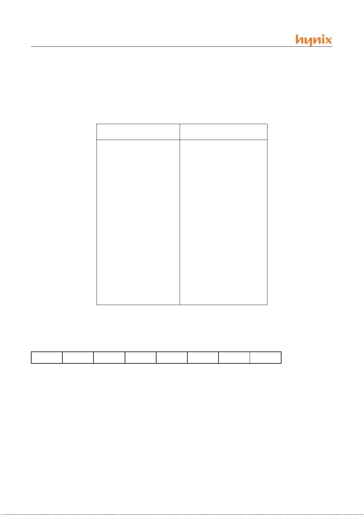
Device na me ROM Size (bytes) RAM size Package
HMS91C8032 32K 1024 bytes 80MQFP Mask ROM version
HMS97C8032 32K bytes OTP 1024 bytes 80MQFP OTP ROM version
NOV., 2001 Ver 1.02 1
Page 5
HMS91C8032/97C8032
1.3 Features
Item Features
ROM 32K x 8-bit
RAM 1K x 8-bit
Instruction Cycle
Instruction Set MCS-51 Micro-controller Compatible Instruction Set
I/O Port CMOS I/O : 62 pins (including 4-open drain ports)
A/D Converter 8-bit resolution x 8-channels
With variable instruction execution time function
1.66µs / 3.33µs / 26.6µs (with main system clock : 7.2MHz)
366.2µs (with sub-system clock : 32.768KHz)
Serial Interface
Timer/Counter
Buzzer(Beep) Output 1.2KHz (fx/6000), 2.4KHz (fx/3000), 4.5KHz (fx/1600), 8.0KHz (fx/900)
Interrupt Source 7 External, 11 Internal Sources
PLL
Frequency
Synthesizer
Frequency Counter
Standby Function
Division Mode
Reference
Frequency
Charge Pump Error out : EO pin
Phase Detector Unlock detectable by program
Reset
3-wire serial I/O mode : 2 channels
Full duplex UART : 1 channel
Five 16-bit timers/event counters
Dedicated Watchdog timer
Direct divis ion mode (VCOL pin)
Pulse swallow mode (VCOH and VCOL pins)
13 types selected by program
1, 1.25, 2.5, 3, 5, 6.25, 9, 10, 12.5, 18, 20, 25, 50KHz
Frequency Measur em en t
AMIFC pin : for 450KHz count
FMIFC pin : for 10.7MHz count
Idle mode
Power-down mode
Reset by RESET pin
Reset by Vdet circuit
Vdet circuit: Detection of less than 2.7V (Normal operation mode)
Power Supply Voltage
System Clock
Package 80 pin plastic MQFP
VDD = 4.5V to 5.5V (with PLL operating)
VDD > 1.8V (Data retention mode)
Main system clock : 7.2MHz
Sub-system clock : 32.768KHz
2 NOV., 2001 Ver 1.02
Page 6

1.4 Pin Description
HMS91C8032/97C8032
Pin
Names
1
2
3
4
5
6
7
8
9
10
11
12
13
14
15
16
17
18
19
20
21
22
23
24
Port
Names
P0.0
P0.1
P0.2
P0.3
P0.4
P0.5
P0.6
P0.7
P1.0
P1.1
P1.2
P1.3
P1.4
P1.5
P1.6
P1.7
P2.0
P2.1
P2.2
P2.3
P2.4
P2.5
P2.6
P2.7
Alternative
s
N-ch
N-ch
N-ch
N-ch
Functions
8-bit general purpose bidirectional
Pin
Input and output mode selected by
8-bit Port Mode Register.
In Input mode, pin can use on-chip
pullup resister by software.
8-bit general purpose bidirectional
Pin
Input and output mode selected by
8-bit Port Mode Register.
In Input mode, pin can use on-chip
pullup resister by software.
8-bit general purpose bidirectional
Pin
Input and output mode selected by
8-bit Port Mode Register.
In Input mode, P2.4~P2.7pin can
use on-chip pullup resister by software. P2.0~P2.3pin have no pullup
Rese
t
LED drive ability. Input
Input
N-channel open drain (P2.0 P2.3)
N-channel open drain voltage :
Max. 6V
Input
25
26
27
28
29
30
31
41
71
32
50
74
33
34
35
36
37
38
39
40
P3.0
P3.1
P3.2
P3.3
P3.4
P3.5
VSS1
VSS2
VSS3
VDD!
VDD2
VDD3
P4.0
P4.1
P4.2
P4.3
P4.4
P4.5
P4.6
P4.7
T0
T1
T2
T3
T4
T2EX
INT0
INT1
INT2
INT3
INT4
INT5
INT6
BEEP
6-bit general purpose bidirectional
Pin
Input and Output mode selected by
8-bit Port Mode Register.
Ground -
DC
Supply Voltage is 5V +/- 10%.
In Power down mode, RAM data guaranteed until 1.8V
All VDD pin is connected in system.
VDD1 : I/O VDD, VDD2 : core VDD, VDD3 : analog VDD
8-bit general purpose bidirectional
Pin
Input and output mode selected by
8-bit Port Mode Register.
In Input mode, pin can use on-chip
pullup resister by software.
P3.0 - P3.5 pin can use Timer
input pin
P4.0 - P4.6 is External Interrupt
input pin.
level/falling detect : 2 pin
level/edge detect : 5 pin
P4.7 is beep clock putput.
Input
Input
-
NOV., 2001 Ver 1.02 3
Page 7

HMS91C8032/97C8032
41
42
43
44
45
46
47
48
49
50
51
52
53
54
55
56
57 TstEn Ground
60 Avref+
61
62
63
64
65
66
67
68
P5.0
P5.1
P5.2
P5.3
P5.4
P5.5
P5.6
P5.7
P6.0
P6.1
P6.2
P6.3
P6.4
P6.5
P6.6
P6.7
P7.0
P7.1
P7.2
P7.3
P7.4
P7.5
P7.6
P7.7
TxD
RxD
SCK1
SO1
SI1
SCK2
SO2
SI2
ANI0
ANI1
ANI2
ANI3
ANI4
ANI5
ANI6
ANI7
8-bit general purpose bidirectional
Pin
Input and output mode selected by
8-bit Port Mode Register.
In Input mode, pin can use on-chip
pullup resister by software.
8-bit general purpose bidirectional
Pin
Input and Output mode selected by
8-bit Port Mode Register.
In Input mode, pin can use on-chip
pullup resister by software.
This pin is oniy ground.
Chip test pin
A/D converter reference voltage input pin
In AD converter, signal from ANI0 ~ ANI7 change to digital signal by reference between AVref+ and VSS.
8-bit general purpose bidirectional
Pin
Input and output mode selected by
8-bit Port Mode Register.
In Input mode, pin can use on-chip
pullup resister by software.
TxD, RxD : Asynchronous serial
data pin
SI1, SI2, SO1, SO2 : Synchronous
serial data pin
SCK1, SCK2 : Clock pin for Synchronous serial data
A/D converter 8-channel analog
input pin
If pin is not used by A/D converter
input, can use to general-purpose
bidirectional pin.
Input voltage in ANI0 - ANI7 is
between Avref+ and VSS.
Input
Input
GND
Input
69 AMIFC AM IF input pin
70 FMIFC FM IF input pin
72 VCOH FM band VCO frequency input pin
73 VCOL AM band VCO frequency input pin
Error output pin in PLL part (charge pump output)
75 EO
76 RESET Chip reset pin. Reset is active high.
77 Xin Crystal oscillator input pin for main system clock
78 Xout Main system clock output pin
79 Xtin Crystal oscillator input pin for Sub system clock
80 Xtout Sub system clock output pin
If tuning freq. = VCO freq., EO pin is floating.
If tuning freq. > VCO freq., EO pin is high.
If tuning freq. = VCO freq., EO pin is low.
4 NOV., 2001 Ver 1.02
Page 8
1.5 Pin Diagram
P0.0
P0.1
P0.2
P0.3
P0.4
P0.5
P0.6
P0.7
P1.0
P1.1
P1.2
P1.3
P1.4
P1.5
P1.6
P1.7
P2.0
P2.1
P2.2
P2.3
P2.4
P2.5
P2.6
P2.7
10
11
12
13
14
15
16
17
18
19
20
21
22
23
24
1
2
3
4
5
6
7
8
9
XTout
XTin
79
80
Open Drain &
}
No Pull-up
25
26
Xout
Xin
78
RESETEOVDD3
76
77
75
74
VCOL
73
VCOH
72
HMS91C8032
HMS97C8032
P2.0~P2.3)
27
28
29
30
31
32
33
VSS3
71
34
FMIFC
70
35
AMIFC
69
36
P7.7/ANI7
68
37
P7.6/ANI6
67
38
P7.5/ANI5
66
39
HMS91C8032/97C8032
P7.4/ANI4
65
64
P7.3/ANI3
63
P7.2/ANI2
62
P7.1/ANI1
61
P7.0/ANI0
60
Avref+
59
VDD2
58
VSS2
57
TSTEN
(Only Ground)
56
P6.7
55
P6.6
54
P6.5
53
P6.4
52
P6.3
51
P6.2
50
P6.1
49
P6.0
48
P5.7/SI0
47
P5.6/SO0
46
P5.5/SCK0
45
P5.4/SI1
44
P5.3/SO1
43
P5.2/SCK1
42
P5.1/RxD
41
P5.0/TxD
40
VSS1
P3.0/T0
P3.1/T1
P3.2/T2
P3.3/T3
P3.4/T4
P3.5/T2EX
VDD1
P4.0/INT0
P4.1/INT1
P4.2/INT2
P4.3/INT3
P4.4/INT4
P4.5/INT5
P4.6/INT6
P4.7/BEEP
Figure 1-1 HMS9XC8032 Pin Diagram
NOV., 2001 Ver 1.02 5
Page 9
HMS91C8032/97C8032
2. MEMORY ORGANIZATION
All HMS91C8032 de vices hav e separ ate add ress sp ace s for p rogram and data memory. The logical separation of program and
data memory allows the data memory to be accessed by 8-bit addresses, which can be quickly stored and manipulated by an 8-bit
CPU.
Program memory (ROM) can only be read, not written to. There
can be up to 32K bytes of program memory. In the
HMS9XC8032 devices, the Program Memory is provided
on-chip.
Data Memory (RAM) occupies a separate address space from
Program Memory. In the HMS9XC8032, the data memory is
on-chip.
Interrupt
Location
008BH
0013H
8 Bytes
000BH
2.1 Program Memory
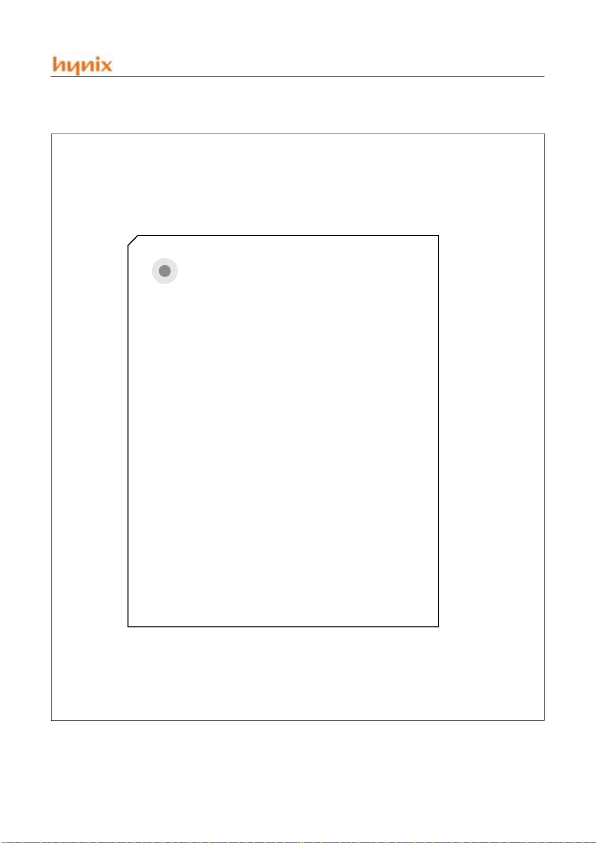
Figure 2-1 shows a map of the lowe r pa r t o f the Pr o gr a m Me mo ry. After reset, the CPU begins executi on from lo cati on 0000 H.
As shown in Figur e 2-2, each in terrupt is assigne d a fixe d location in Program Memory. The interrupt causes the CPU to jump
to that location, wher e it commences ex ecution of the se rvice routine. External Interrupt 0, for example , is assigned to location
0003H. If External Interrupt 0 is going to be used, its service routine must begin at location 0003H. If the interrupt is not going to
be used, its service location is available as general purpose Program Memory.
The interrupt service locations are spaced at 8-byte intervals :
0003H for External Interrupt 0, 000BH for Timer 0, 0013H for
External Interrupt 1, 001BH for Timer 1 and etc. If an interrupt
service routine is short enou gh (as is often the case in control applications), it can reside entirely within that 8-byte interval.
Longer service routines can use a jump instruction to skip over
subsequent interrupt locations, if other interrupts are in use.
Program Memory addresses are always 16bits wide, even though
the actual amount of Program Memory used may be less than 32K
bytes.
7FFFH
0003H
Reset
0000H
Figure 2-2 Interrupt Location of Program Memory
2.2 Data Memory
Figure 2-3, Fi gure 2-6 and Fig ure 2-6 shows the Memory spaces
available to the HMS9XC8032 use r. HMS9XC8032 can address
up to 1kbytes of data memory . 10bits address is config ured as follows.
10bits address for READ memory operation = 2bits of RDPG +
8bits of implied address in instruction
10bits address for WRITE memory operation = 2bits of WRPG +
8bits of implied address in instruction
(Where, 0 =< RDPG, WRPG =< 6)
(CAUTIONS: A valid value which can be stored in RD PG and
WRPG must be from 0 to 6. 7 is reserved for indirect addressable
memory region.( upper 128byt es region) A progr ammer who set
RDPG/WRPG to 7 or greater than 7 will get the invalid memory
operation results. )
7FH
Accessible
by Direct
Addressin g
Accessible
by Direct
Addressin g
RDPG
WRPG
32Kbyte
0000H
Upper
128
00H
7FH
Lower
128
00H
Accessible
by Indirect
Addressing
Only
Accessible
by Direct
Addressing
Figure 2-1 Program Mamory
Figure 2-3 Data Memory Structure
6 NOV., 2001 Ver 1.02
Page 10
HMS91C8032/97C8032
Data memory consists of 7 pages, and each page can store
128bytes. According to the value of RDPG(FCH) and WRPG(FDH), HMS9XC8032 selects working memory page. Figure
2-4 shows the generation method of in ternal data memory address. For example, to read from data memory, HMS9XC8032
references the content of RDPG, generates 10bits address and ac-
RDPG [2 : 0]
3
Implied address of instruction
7
WRPG [2 : 0]
3
Implied address of instruction
7
RAM Read Address
10
RAM Write Address
10
cesses the corresponding data. The following two cases are
equivalent.
MOV 00H, A 1)
MOV R0, A 2)
FFH
No Bit-Addressable Spaces
80H
Figure 2-5 Upper 128bytes of Internal RAM
Figure 2-4 Data Memory Address Generation Method
7FH
Bank
Select
Bits
in PSW
2FH
20H
11
18H
10
10H
01
08H
00
0
1FH
17H
0FH
07H
Bit-Addressable
Space
(Bit Addresses 0-7F)
4 Banks of
8 Registers
R0-R7
Reset Value of
Stack Pointer
Page 0
Figure 2-6 Page0 ~ Page6 of Internal RAM
2.3 Special Function Register
Unlike Intel 805X series, HMS9XC8032 has two SFR pages. If
the content of SFRPG (address:FFH) is clear to 00H(01H),
HMS9XC8032 assumes working SFR page to SFR page 0(1).
Byte-addressing only registers in SFR pages have the same address in each SFR pages, but bit addressing registers in SFR page
7FH
Bank
Select
Bits
in PSW
2FH
20H
11
18H
10
10H
01
08H
00
0
1FH
17H
0FH
07H
Bit-Addressable
Space
(Bit Addresses 0-7F)
4 Banks of
8 Registers
R0-R7
Reset Value of
Stack Pointer
Page 6
0 and SFR page 1 are different except ACC, B and PSW.
The Port Data registers are located to SFR page1, and the Periph-
eral Control registers to SFR page0. Refer to "4.2 Special Function Registers" on page 19.
NOV., 2001 Ver 1.02 7
Page 11
HMS91C8032/97C8032
HMS91C8032/HMS97C8032 Description
3. INSTRUCTION SET
The HMS9XC8032 instruction set is optimized for 8-bit control applications. It provides a variety of fast addressing modes for accessing
the internal RAM to facilitate byte opera tions on small data structure s. The instru ction set p rovid es extensi ve suppo rt for one - bit variables
as a separate data type, allowing direc t bit manipulation in control and logic syst ems that require Bool ean processing.
3.1 Program Status Word
The Program Status Word (PSW) contains several status bits that
reflect the current stat e of the CPU. T he PSW, sho wn in Figu re
3-1, resides in the SFR space. It contains the Carry bit, the Auxiliary Carry (for BCD operations), the two register bank select
bits, the Overflow flag, a Parity bit, and two user-definable status
flags.
The Carry bit, other than serving the functions of a Carry bit in
arithmetic o perations, also serves as the “A ccumulator” for a
number of Boolean operations.
AC -CY F0 RS0 OV P
Carry flag receives carry out
from bit 7 of ALU operands
Auxiliary carry flag receives
carry out from bit 3
of addition operands
General purpose status flag
Register bank select bit 1
PSW 7
PSW 6
PSW 5
PSW 4
Figure 3-1 PSW (Program Status Word) Register in HMS9XC8032 Devices
RS0 and RS1 are used to select one of the four register banks.
Each register bank composed of eight registers.(R0 to R7) The
selection of a register bank is made at execution time.
The parity bit reflects the nu mbe r o f 1s in th e Accu m ulato r: P= 1
if the Accumulator contains an odd number of 1s, and P = 0 if the
Accumulator contains an even number of 1s. Thus the number of
1s in the Accumulator plus P is always eve n. Two bits in the PS W
are uncommitted and may be used as gen eral-purpose status
flags.
RS1
PSW 0
Parity of accumulator
set by hardware to 1 if it
contains an odd number
of 1s; otherwise it is
reset to 0
PSW 1
User-definable flag
PSW 2
Overflow flag set by
arithmetic operation
PSW 3
Register bank select bit 0
Direct Addressing
In direct addressing the op erand is specif ied by an 8-bit address
field in the instruction. Only interna l Data RAM an d SFRs can be
directly addressed.
Indirect Addressing
In indirect addressing the instruction specifies a register which
contains the address of the operand. Both internal and external
RAM can be indirectly addressed.
3.2 Addressing Modes
The addressing modes in the HMS9XC8032 instruction set are as
follows:
The address register for 8-bit addresses can be R0 or R1 of the selected bank, or the Stack Pointer. The address register for 16-bit
addresses can only be the 16-bit "data po inter" register, DPTR.
8 NOV., 2001 Ver 1.02
Page 12
HMS91C8032/97C8032
Register Instructions
The register banks, containing registers R0 through R7, can be
accessed by certain instructions which carry a 3-bit register specification within the opcode o f the instruction. Inst ructions that access the registers this way are code efficient, since this mode
eliminates an address byte. When the in struction is executed , one
of the eight registers in the selected bank is accessed. One of four
banks is selected at execution time by the two bank sel ect bits in
the PSW.
Register-Specific Instructions
Some instructions are specific to a certain register. For example,
some instructions always operate on the Accumulator, or Data
Pointer, etc., so no address byte is needed to point to it. The opcode itself does that. Instructions that refer to the Accumulator as
A assemble as accumulator specific opcodes.
Immediate Constants
The value of a constant can follow the opcode in Program Memory. For example,
MOV A, #100
loads the Accumulator with the decimal number 100. The same
number could be specified in hex digits as 64H.
Indexed Addressing
Only Program Memory can be accessed with indexed addressing,
and it can be re ad. T h is addr es sing mo de i s i nte nde d for r eadi n g
look-up tables in Program Memory. A 16-bit base register (either
DPTR or the Program Cou nter) points to the base of the table, and
the Accumulator is set up with the table entry number.
The address of the ta ble entry in Pr ogram Memo ry is fo rmed by
adding the Accumulator data to the base pointer.
Another type of indexe d addressing is used in the "case jump" in struction. In this case the destination a ddress of a jump instruction
is computed as the sum of th e base po inter an d the Ac cumul ator
data.
3.3 Arithmetic Instructions
The arithmetic instructions is listed in Table 3-1. The table indicates the addressing modes that can be used with each instruction
to access the <byte> operand. For example, the ADD A, <byte>
instruction can be written as:
ADD a, 7FH (direct addressing)
ADD A, @R0 (indirect addressing)
ADD a, R7 (register addressing)
ADD A, #127 (immediate constant)
Note that any byte in the internal Data Memory space can be incremented without going through the Accumulator.
One of the INC instructions operates on the 16-bit Data Pointer.
The Data Pointer is used to genera te 16-b it addre sses for extern al
memory, so being able to increment it in one 16-bit operations is
a useful feature.
The MUL AB instruction multiplies the Accumulato r by the data
in the B register and puts the 16-bit product into the concatenated
B and Accumulator registers.
The DIV AB instruction divides the Accumulator by the data in
the B register and leaves the 8-bit quotient in the Accumulator,
and the 8-bit remainder in the B register.
MNEMONIC OPERATION ADDRESSING MODES
Dir Ind Reg Imm
ADD A,<byte> A = A+<byte> X X X X
ADDC A,<byte> A = A+<byte>+C X X X X
SUBB A,<byte> A = A-<byte>-C X X X X
IN C A = A+1 Accumulator only
INC <byte> <byte> = <byte>+1 X X X
INC DPTR DPTR = DPTR+1 Data Pointer only
DEC A A = A-1 Accumulator only
DEC <byte> <byte> = <byte>-1 X X X
MUL AB B:A = B x A ACC and B only
DIV AB
DA A Decimal Adjust Accumulator only
A = Int[A/B]
B = Mod[A/B]
Table 3-1 HMS9XC8032 Arithmetic Instructions
ACC and B only
NOV., 2001 Ver 1.02 9
Page 13
HMS91C8032/97C8032
Oddly enough, DIV AB finds less use in arithmetic "divide" routines than in radix conversions and programmable shift operations. An exam ple of the use of DIV AB in a ra dix conver sion will
be given later. In shift operations, dividing a number by 2n shifts
its n bits to the right. Using DIV AB to p erform the div ision completes the shift in 4µs and leaves the B register holding the bits
that were shifted out. The DA A instructio n is for BCD arithmetic
operations. In BCD arithmetic, ADD and ADDC instructions
should always be followed by a DA A op eration, to ensure that
the result is also in BCD. Note th at DA A will n ot convert a bi nary number to BCD. The DA A operation prod uces a meaning ful
The addressing modes tha t can be used to a ccess t he <b yte> o perand are listed in Table 3-2.
The ANL A, <byte> instruction may take any of the forms:
ANL A,7FH(direct addressing)
ANL A, @R1 (indirect addressing)
ANL A,R6 (register addressing)
ANL A,#53H (immediate constant)
Note that Boolean operations can be performed on any byte in the
internal Data Memory space without going throug h the Accumulator. The XRL <byte>, #data instruction, for example, offers a
quick and easy way to invert port bits, as in
XRL P1, #0FFH.
result only as the second step in the addition of two BCD bytes.
3.4 Logical Instructions
Table 3-2 shows list of HMS9XC8032 logical instructions. The
instructions that perform Boolean operations (AND, OR, Exclusive OR, NOT) on bytes perf orm t he opera tion on a bit-by -bit basis. That is, if the Accumulator contains 0011 0101B and byte
contains 01010011B, then :
ANL A, <byte>
will leave the Accumulator holding 00010001B.
If the operation is in response to an in terrupt, n ot using th e Accu mulator saves the time and effort to push it onto the stack in the
service routine.
The Rotate instructions (RL A, RLC A, etc.) shift the Accumulator 1 bit to the left or right. For a left rotation, the MSB rolls into
the LSB position. For a righ t rotation, the LSB rolls i nto the MSB
position.
The SWAP A instruc tion in terchange s the high and low ni bbles
within the Accumulator. This is a useful operation in BCD manipulations. For example, if the Accumulator contains a binary
number which is known to be less than 100, it can be quickly converted to BCD by the following code:
MNEMONIC OPERATION ADDRESSING MODES
Dir Ind Reg Imm
ANL A,<byte> A = A .AND. <byte> X X X X
ANL <byte>,A <byte> = <byte> .AND. A X
ANL <byte>,#data <byte> = <byte> .AND. #data X
ORL A,<byte> A = A .OR. <byte> X X X X
ORL <byte>,A <byte> = <byte> .OR. A X
ORL <byte>,#data <byte> = <byte> .OR. #data X
XRL A,<byte> A = A .XOR. <byte> X X X X
XRL <byte>,A <byte> = <byte> .XOR. A X
XRL <byte>,#data <byte> = <byte> .XOR. #data X
CRL A A = 00H Accumulator only
CPL A A = .NOT. A Accumulator only
RL A Rotate ACC Left 1 bit Accumulator only
RLC A Rotate Left through Carry Accumulator only
RR A Rotate ACC Right 1 bit Accumulator only
RRC A Rotate Right through Carry Accumulator only
SWAP A Swap Nibbles in A Accumulator only
Table 3-2 HMS9XC8032 Logical Instructions
10 NOV., 2001 Ver 1.02
Page 14
HMS91C8032/97C8032
MOVE B,#10
DIV AB
SWAP A
ADD A,B
Dividing the number by 1 0 lea ves th e tens d igit in the low nibble
of the Accumulator, and the ones digit in the B register. The
SWAP and ADD instructions move the tens digit to the high nibble of the Accumulator, and the ones digit to the low nibble.
3.5 Data Tr ansfers
Internal RAM
Table 3-3 shows the menu of instructions that are available for
moving data around within the internal memory spaces, and the
addressing modes that can be used with each one.
The MOV <dest>, <src> instruction allo ws data to be transferred
between any two internal RAM or SFR locations without going
through the Accumulator. Remember, the Upp er 128 bytes of
data RAM can be accessed only by indirect addressing, and SFR
space only by direct addressin g.
Note that in HMS9XC8032 devices, the stack res ides in on-chi p
RAM, and grows upwards. The PUSH instruction first increments the Stack Pointer (SP), then copies the byte into the stack.
PUSH and POP use only direct addressing to identify the byte being saved or restored, but t he stack itsel f is accessed by i ndirect
addressing using the SP register. This means the stack can go into
the Upper 128 bytes of RAM, if they are implemented, but not
into SFR space.
The Data Transfer instructions include a 16 -b it MOV th at can b e
used to initialize the Data Pointer (DPTR) for look-up tables in
Program Memory.
The XCH A, <byte> instruction causes the Accumulator and addressed byte to exchange data. The XCHD A, @Ri instruction is
similar, but only the low nibbles are involved in the exchange.
To see how XCH and XCHD can be used to facilitate da ta manipulations, consider first the problem of shifting and 8-digit BCD
number two digits to the right. Figure 3-2 shows how this can be
done using XCH instructions. To aid in understanding how the
code works, the contents of the registers that are holding the BCD
number and the content of the Accumulator are shown alongside
each instruction to indicate their status after the instruction has
been executed.
After the routine has been executed, the Accumulator contains
the two digits that were shifte d out on th e right. Doin g the routin e
with direct MOVs uses 14 code bytes. The sa me operation with
XCHs uses only 9 bytes and execut es almost twice as fast.
To right-shift by an odd number of digits, a one-digit must be executed.
Figure 3-3 shows a sample of code that will right-shift a BCD
number one digit, using the XCHD instruction. Again, the contents of the registers holding the number and of the accumulator
are shown alongsid e each instruction.
MNEMONIC OPERATION ADDRESSING MODES
Dir Ind Reg Imm
MOV A,<src> A = <src>
MOV <dest>,A <dest> = A
MOV <dest>,<src> <dest> = <src>
MOV DPTR,#data16 DPTR = 16-bit immediate constant
PUSH <src> INC SP:MOV “@SP”, <src>
POP <dest> MOV <dest>, “@SP”:DEC SP
XCH A,<byte> ACC and <byte> exchange data X X X
XCHD A,@Ri ACC and @Ri exchange low nibbles X
Table 3-3 Data Transfer Instruction that Access Internal Data Memory Space
XXXX
XXX
XXXX
X
X
X
NOV., 2001 Ver 1.02 11
Page 15
HMS91C8032/97C8032
2B
2A
12
MOV A,2EH
MOV 2EH,2DH
MOV 2DH,2CH
MOV 2CH,2BH
MOV 2BH,#0
A. Using d irect MOVs: 14 bytes, 9 us
CLR A
XCH A,2BH
XCH A,2CH
XCH A,2DH
XCH A,2EH
B. Using XCHs: 9 bytes, 5us
00
12
00
12
00
12
00
00
00
2B
2A
12
00
00
00
00
00
00
00
00
00
Figure 3-2 Shifting a BCD Number Two Digits to the
Right
2A
MOV R1,#2EH
MOV R0,#2DH
00
00
2D 2E ACC
2C
78
56
34
56
34
34
34
34
12
34
12
2D 2E ACC
2C
56
34
56
34
56
12
34
12
34
12
2D 2E
2C
2B
1212343456567878XX
78
56
78
56
78
56
78
56
78
78
00
78
12
78
34
78
56
56
78
ACC
XX
leaves the last byte, location 2EH, holding the last two digits of
the shifted number. The p ointers are decre mented, and the loop is
repeated for location 2DH. The CJNE instruction (Compare and
Jump if Not equal) is a loop control that will be described later.
The loop executed from LOOP to CJNE for R1 = 2EH, 2DH,
2CH, and 2BH. At that point the digit that was originally shifted
out on the right has pr opagated to location 2AH. Since that location should be left with 0s, the lost di git is moved to the Accum ulator.
External RAM
HMC9XC8032 series do NOT support external RAM access
mode.
3.6 Lookup Tables
Table 3-4 shows the two instructions that are available for reading lookup tables in Program Memory. Since these instructions
access only Program Memory, the lookup tables can only be read,
not updated.
The mnemonic is MOVC for "move constant." The first MOVC
instruction in Table 3-1 can accommodate a table of up to 256 entries numbered 0 through 25 5. T he numbe r of the desired entry is
loaded into the Accumu lator, and the Data Poi nter is set up to
point to the beginning of the table. Then:
MOVC A, @A+DPTR
loop for R1 = 2EH
MOV A,@R1
LOOP:
XCHD A,@R0
SWAP A
MOV @R1,A
DEC R1
DEC R0
CJNE R1,#2AH,LOOP
00
12
00
12
00
12
00
12
00
12
00
12
56
34
58
34
58
34
58
34
58
34
58
34
78
78
76
78
67
78
67
67
67
67
67
67
copies the desired table entry into the Accumulator.
The other MOVC instruction works the same way, exce pt the
Program Counter (PC) is used as the t able base, and the table is
accessed through a subroutine. First the number of the desired entry is loaded into the Accumulator, and the subroutine is called:
MOV A , ENTRY NUMBER
loop for R1 = 2DH:
loop for R1 = 2CH:
loop for R1 = 2BH:
CLR A
XCH A,2AH
00
00
08
000801
38
12
23
18
23
01
23
01
23
67
45
45
45
45
45
45
67
23
67
01
67
00
67
08
CALL TABLE
The subroutine "TABLE" would look like this:
TABLE: MOVC A , @A+PC
RET
Figure 3-3 Shifting a BCD Number One Digits to the
Right
The table itself immediately follows the RET (re turn ) instruc ti on
is Program Memory. This type of table can hav e up to 255 entries,
numbered 1 through 255. Number 0 cannot be used, because at
the time the MOVC instruction is executed, the PC contains the
First, pointers R1 and R0 are set up to point to the two bytes con taining the last four BCD digits. Then a loop is executed which
address of the RET instruction. An entry numbered 0 would be
the RET opcode itself.
MNEMONIC OPERATION
MOVC A, @A+DPTR Read program memory at (A + DPTR)
MOVC A, @A+PC Read program memory at (A + PC)
Table 3-4 Table B-4 HMS9XC8032 Data Transfer Instruction that Access Internal Data Memory Spcace
12 NOV., 2001 Ver 1.02
Page 16

3.7 Boolean Instructions
HMS9XC8032 devices contain a complete Boolean (single-bit)
processor. One page of the int ernal RAM contains 128 addressable bits, and the SFR space can support up to 128 addressab le
bits as well. All of the port lines are bit-addressable, and each one
can be treated as a separate single-bit port. The instructions that
access these bits are not just conditional branches, but a complete
menu of move, set, clear, com plement, OR and AND instructions. These kind s of bi t operat ions ar e not ea sily obt ained in other architectures with any amount of byte-oriented software.
The instruction set for the Boolean processor is shown in Table
3-5. All bits accesses are by direct ad dressing.
Bit addresses 00H through 7FH are in the Lower 128, and b it addresses 80H through FFH are in SFR space.
Note how easily an inte rna l fl a g can be mo ve d to a port pin:
MOV C,FLAG
MOV P1.0,C
In this example, FLAG is the name of any addressable bit in the
Lower 128 or SFR space. An I/O line (the LSB of Port 1, in this
case) is set or cleared depending on whether the flag bit is 1 or 0.
HMS91C8032/97C8032
Note that the Boolean instruction set includ es ANL and ORL op-
erations, but not the XRL (Exclusive OR) operation. An XRL op-
eration is simple to implement in software. Suppose, fo r example,
it is required to form the Exclusive OR of two bits:
C = bit 1 .XRL. bit2
The software to do that could be as follows:
MOV C , bit1
JNB bit2, OVER
CPL C
OVER: (continue)
First, bit1 is moved to th e Car ry. If bit2 = 0, then C n ow co nta in s
the correct result. That is, bit1 .XRL. bit2 = bit1 if bit2 = 0. On
the other hand, if bit2 = 1, C now contains the complement of the
correct result. It need only be inverted (CPL C) to complete the
operation.
This code uses the JNB instruction, one of a series of bit-test in-
structions which execute a jump if the addressed bi t is set (JC, JB,
JBC) or if the addressed bit is not set (JNC, JNB). In the above
case, bit2 is being tested, and if bit2 = 0, the CPL C instruction is
jumped over.
The Carry bit in the PSW i s used as the sin gle-bit Accumul ator of
the Boolean processor. Bit instructions that refer to the Carry bit
as C assemble as Carry-specific instructions (CLR C, etc.). The
Carry bit also has a direct address, since it resides in the PSW register, which is bit-addressable.
MNEMONIC OPERATION
ANL C,bit C = A .AND. bit
ANL C,/bit C = C .AND..NOT. bit
ORL C,bit C = A .OR. bit
ORL C,/bit C = C .OR..NOT. bit
MOV C,bit C = bit
MOV bit,C bit = C
CLR C C = 0
CLR bit bit = 0
SETB C C = 1
SETB bit bit = 1
CPL C C = .NOT.C
CPL bit bit = .NOT.bit
JC rel Jump if C = 1
JNC rel Jump if C = 0
JB bit,rel Jump if bit = 1
JNB bit,rel Jump if bit = 0
JBC bit,REL Jump if bit = 1;CLR bit
Table 3-5 Table B-5 HMS9XC8032 Boolean Instructions
JBC executes the jump if the addresse d bit is set , and also clears
the bit. Thus a flag can be tested and cleared in one operation. All
the PSW bits are directly addressable, so th e Parity bit, or the gen-
eral-purpose flags, for example, are a lso available to the bit-test
instructions.
3.8 Relative Offset
The destination address for these jumps is specified to the assem-
bler by a label or by an actual address in Program memory. How-
ever, the destination address assembles to a relative offset byte.
This is a signed (two's complement) offset byte which is added to
the PC in two's complement arithmetic if the jump is executed.
The range of th e jump is the refore - 128 to +127 Program Me mory
bytes relative to the first byte following the instruction.
3.9 Jump Instructions
Table 3-6 shows the list of unconditional jumps.
MNEMONIC OPERATION
JMP addr Jump to addr
JMP @A+DPTR Jump to A+DPTR
CALL addr Call subroutine at addr
RET Return from subroutine
RETI Return from interrupt
NOP No operation
Table 3-6 Unconditional Jumps in HMS9XC8032
Devices
NOV., 2001 Ver 1.02 13
Page 17

HMS91C8032/97C8032
The table lists a single "JMP add" instruct ion, but in fact there are
three SJMP, LJMP, and AJMP, which differ in the format of the
destination address. JMP is a generic mnemonic which can be
used if the programmer does not care which way the jump is encoded.
The SJMP instruction encodes the destination address as a relative offset, as described above. The instruction is 2 bytes long,
consisting of the opcode and the relative offset byte. The jump
distance is limited to a range of -128 to +12 7 bytes relative to the
instruction following the SJMP.
The LJMP instruction encodes the destination address as a 16-bit
constant. The instruction is 3 bytes long , consisting o f the opcode
and two address bytes. Th e dest inati on ad dress c an b e an ywhe re
in the 64K Program Memory space.
The AJMP instruction encodes the destination add ress as an
11-bit constant. The instruction is 2 bytes long, consisting of the
opcode, which itself contains 3 of the 11 address bits, followed by
another byte containing the low 8 bits of the de stination address.
When the instruction i s ex ecu te d, the s e 11 b its a re si mply sub s tituted for the low 11 bits in the PC. The hig h 5 bits sta y the same .
Hence the destination has to be within the same 2K block as the
instruction following the AJMP.
In all cases the programmer specifies the destination address to
the assembler in the same way: as a label or as a 16-bit constant.
The assembler will put the destination address into the correct
format for the given instruction. If the format required by the instruction will not support t he di stance to the specified destin ation
address, a "Destination out of range" message is written into the
List file.
Table 3-1 shows a single "CALL addr" instruction, but there are
two of them, LCALL and ACALL, which differ in the format in
which the subroutine address is give n to the CPU. CALL is a g e-
neric mnemonic whi ch can be used if the progr ammer does not
care which way the address is encoded.
The LCALL instruction uses the 16-bit address format, and the
subroutine can be anywhere in the 64K P r ogram Memory space.
The ACALL instruction uses the 11-bit format, and the subrou-
tine must be in the same 2K b lock as the i nstruction fo llowing the
ACALL.
In any case, the programmer specifies the subroutine address to
the assembler in the same way: as a label or as a 16-bit constant.
The assembler will put the address into the correct form at for th e
given instructions .
Subroutines should end with a RET instruction, which returns ex-
ecution to the instruction following the CALL.
RETI is used to return from an interrupt service routine . The only
difference between RET and RETI is that RETI tells the interrupt
control system that the interrupt in progress is done. If there is no
interrupt in progress at the time RETI is exec ut ed, th en th e RETI
is functionally identical to RET.
Table 3-7 shows the list of conditional jumps available to the
HMS9XC8032 user. All of these jumps specify the destination
address by the relative offset me thod, and so are limi ted to a jump
distance of -128 to +127 bytes from the instruction following the
conditional jump instruction. Im portant to note, however, th e user
specifies to the assembler the actual destination address the same
way as the other jumps: as a label or a 16-bit constant.
The JMP @A+DPTR instruction supports case jumps. The destination address is computed at exec ution time as the su m of the
16-bit DPTR register and the Accumulator. Typically. DPTR is
set up with the address of a jump table. In a 5-way branch, for example, an integer 0 thro ugh 4 is loade d into the Accumul ator. The
code to be executed might be as follows:
MOV DPTR,#JUMP TABLE
MOV A,INDEX_NUMBER
RL A
JMP @A+DPTR
The RL A instruction converts the index number (0 through 4) to
an even number on the r ange 0 thro ugh 8, be cause eac h entry in
the jump table is 2 bytes long:
JUMP TABLE:
AJMP CASE 0
AJMP CASE 1
AJMP CASE 2
AJMP CASE 3
AJMP CASE 4
There is no Zero bit in t he PSW . The JZ an d JNZ instruc tions test
the Accumulator data for that condition.
The DJNZ instruction (Decrement and Jump if Not Zero) is for
loop control. To execute a loop N times, load a counter byte with
N and terminate the loop with a DJNZ to the beginning of the
loop, as shown below for N = 10:
MOV COUNTER,#10
LOOP:(begin loop)
•
•
•
(end loop)
DJNZ COUNTER, LOOP
(continue)
.
The CJNE instruction (Compare and Jump if Not Equal) c an also
be used for loop control as in F igure 12. Two bytes are specified
in the operand field o f th e instru c tio n. The j um p is exe cute d on ly
if the two bytes are not equal. In the example of Figu re B-3 Shift-
ing a BCD Number One Digits to the Right, the two bytes were
data in R1 and the constant 2 AH. The initia l data in R1 was 2EH.
14 NOV., 2001 Ver 1.02
Page 18
HMS91C8032/97C8032
MNEMONIC OPERATION ADDRESSING MODES
DIR IND REG IMM
JZ rel Jump if A = 0 Accumulator only
JNZ rel Jump if A ≠ 0 Accumulator only
DJNZ <byte>,rel Decrement and jump if not Zero X X
CJNE A,<byte>,rel Jump if A ≠ <byte> X X
CJNE <byte>,#data,rel Jump if <byte> ≠ #data X X
Table 3-7 Conditional Jumps in HMS9XC8032 Devices
Every time the loop was executed, R1 was d ecremented, and the
looping was to continue until the R1 data reached 2AH.
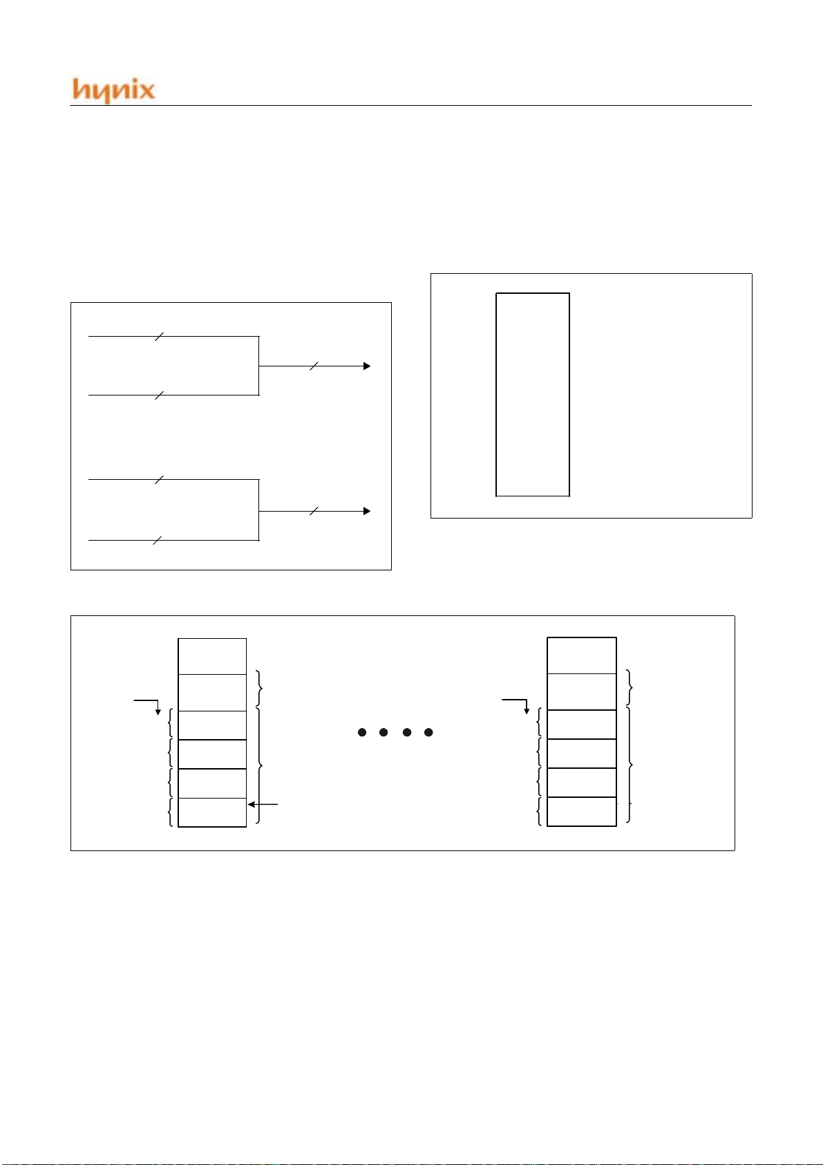
XTAL2
Another application of this instruction is in "greate r than, less
than" comparisons. The two bytes in the operand field are taken
as unsigned integers. If the first is less than the second, then the
Carry bit is set (1). If the first is greater than or equal to the second, then the Carry bit is cleared
Quartz crysta l
or ceramic
resonator
C1
C2
Xout (XTout)
Xin (XTin)
XTAL1
3.10 CPU Timing
All HMS9XC8032 microcontrollers have an on-chip oscillator
which can be used if desired as the clock source for the CPU. To
use the on-chip oscillator, connect a crystal or ceramic resonator
between the Xout (XTout) an d Xin(XTin) pi ns of the mi crocontroller, and capacitor s to gr ound as sh own in F igure 3-4 Using the
On-Chip Oscillator.
Examples of how to drive the clock with an extern al oscillato r are
shown in Figure 3-5 . In the CMOS dev ices (HMS9XC80 32, etc.) ,
the signal at the Xout(XTout) pin drives the internal clock generator. The internal clock ge nerat or defi nes t he sequ ence o f st ates
that make up the HMS9XC80 32 machine cycle.
Main Clock
Xin, Xout : 7.2 MHz
Sub Clock
XTin, XTout : 32.768 KHz
Figure 3-4 sing the On-Chip Oscillator
EXTERNAL
OSCILLATOR
SIGNAL
CMOS GATE
Figure 3-5 Using an External Clock
Vss
DTS3
NC
XTAL1
Xout (XTout)
XTAL2
Xin (XTin)
Vss
NOV., 2001 Ver 1.02 15
Page 19
HMS91C8032/97C8032
3.1 1 Machine Cycles
A machine cycle consists of a sequence of 6 states, numbered S1
through S6. One machine cycle period vary according to the SCMOD register value. Refer to Figure 3-6
Each state is divided into a Phase 1 half and a Phase 2 half. State
Sequence in HMS9XC8032 Devices shows that fetch/execute sequences in states and phases for vari ous kinds of instructi ons.
Normally two progra m fetches are gene rated during each machine cycle, even if the instruction being executed doesn't require
it. If the instruction being executed doesn't need more code bytes,
the CPU simply ignores the e xtra fetc h, a nd the Pro gram Coun ter
is not incremented.
Execution of a one-cycle instruction (Figure 3-6) begins during
State 1 of the machine cycle, when th e opc od e is latche d into the
Instruction Register. A second fetch occurs during S4 of the same
machine cycle. Execution is complete at the end of State 6 of this
machine cycle.
Osc.
CPU Clock
(XTAL2)
(f
)
CPU
S1 S2 S3 S4 S5 S6 S1 S2 S3 S4 S5 S6 S1
P1P2 P1P2 P1P2 P1P2 P1P2 P1P2 P1P2 P1P2 P1P2 P1P2 P1P2 P1P2
Read opcode.
S1
S2
S3
S4
a. 1-byte, 1-cycle instruction, e.g., INC A
Read opcode.
S1
S2
S3
S4
b. 2-byte, 1-cycle Instruction, e.g., ADD A, #data
Read opcode.
Read next
opcode
(discard).
S5
S6
Read 2nd byte.
S5
S6
Read next
opcode (discard)
P1P2
Read next opcode again.
Read next opcode.
Read next opcode again.
S1
S2
S3
S4
S5
S6
S1
S2
S3
S4
S5
S6
c. 1-byte, 2-cycle instruction, e.g., INC DPTR
Figure 3-6 State Sequence in HMS9XC8032 Devices
16 NOV., 2001 Ver 1.02
Page 20
HMS91C8032/97C8032
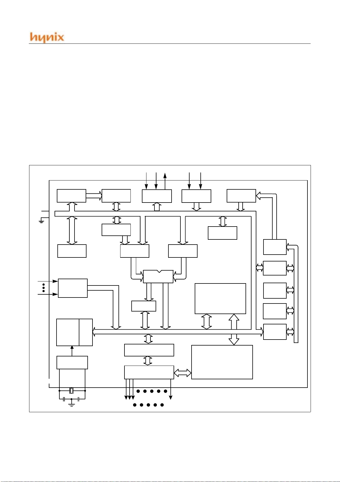
4. HARDWARE DESCRIPTION
This chapter provides a detailed description of the HMS9XC8032 microcontroller (see Figure 4-1) included in this description are the:
• Clock Genernation Block
• IF Counter
• Special Function Registers
• Timers/Counters
• Serial Interface (UART)
• Standard Serial Interface (SI0 1, SIO2)
• Port Structure
• Watch Dog Timer
•Buzzer
RAM Address
Register
Vcc
Vss
B
Register
RAM
ACC
TMP2 TMP1
•PLL
• ADC
• Interrupts
• Reset
• Power-On Reset
• Power-Saving Modes
• On-Chip Oscillators
Stack
Pointer
ROM
Program
Address
Register
XTAL1
Timing
And
Control
Oscillator
Instruction
XTAL2
Buffer
ALU
PC
Peripheral Control
PSW
Register
Register Blocks
Incrementer
Program
Counter
DPTR
Ports Latchs
Peripheral Blocks
(Interrupt, SIOs, Timers, etc)
Ports Drivers
P0 P7
Figure 4-1 HMS9XC8032 Architecture
NOV., 2001 Ver 1.02 17
Page 21
HMS91C8032/97C8032
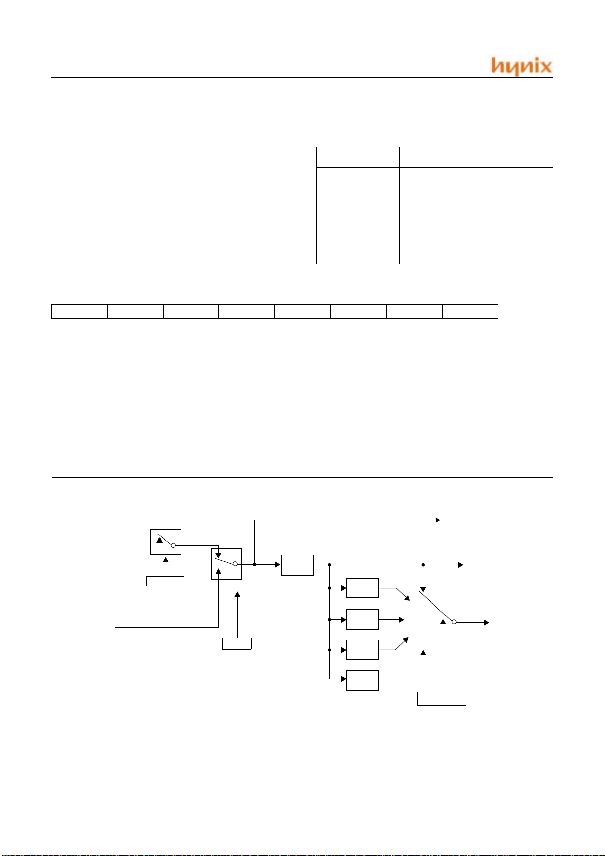
4.1 Clock Generation Block
Software can control the system clock speed of HMS91C8032
with the SCMOD register. the SCMOD register determine system clock speed and clock source. Figure 4-3 shows the block diagram of the system clo c k generation block.
Guideline on the CPU clock speed
For determining the speed of CPU clock(f
constraints should be satisfied.
The maximum counting rate of timer0~4 in counter mode,
should be less than or equal to (1/6)f
CPU
The maximum timer clock rate of timer0~4 in timer mode
should be less than or equal to (1/2)f
CPU
), the following
CPU
SCMOD: SELECT CLOCK MODE. : 80H
- - - SCSTOP SCSW SCMOD2 SCMOD1 SCMOD0
- SCMOD.7 Reserved for future use *
- SCMOD.6 Reserved for future use *
- SCMOD.5 Reserved for future use *
SCSTOP SCMOD.4 Software control of the main system oscillator. A logic 1 pulls down the main
system oscillator (7.2MHz).
SCSW SCMOD.3 Software switch control betwee n main system oscillator and sub syst em oscillator.
A logic 1 switches sub syst em oscillator (32.768KHz).
SCMOD2 SCMOD.2 See NOTES
SCMOD1 SCMOD.1 See NOTES
SCMOD0 SCMOD.0 See NOTES
NOTE:
SCMOD[2:0] Select system clock
0xxfxx
1 0 0 fxx / 2
1 0 1 fxx / 4
1 1 0 fxx / 8
1 1 1 fxx / 16
PLL Clock
f
MOSC
(Main Oscillator Clock)
f
SOSC
(Sub Oscillator Clock)
SCSTOP
0
1
SCSW
f
OSC
(Oscillator
Clock)
1/2
f
XX
1/2
1/4
1/8
1/16
SCMOD1 ,2 ,3
Watchdog Clock
f
CPU
(CPU Clock)
Figure 4-2 System Clock Generation Block
18 NOV., 2001 Ver 1.02
Page 22
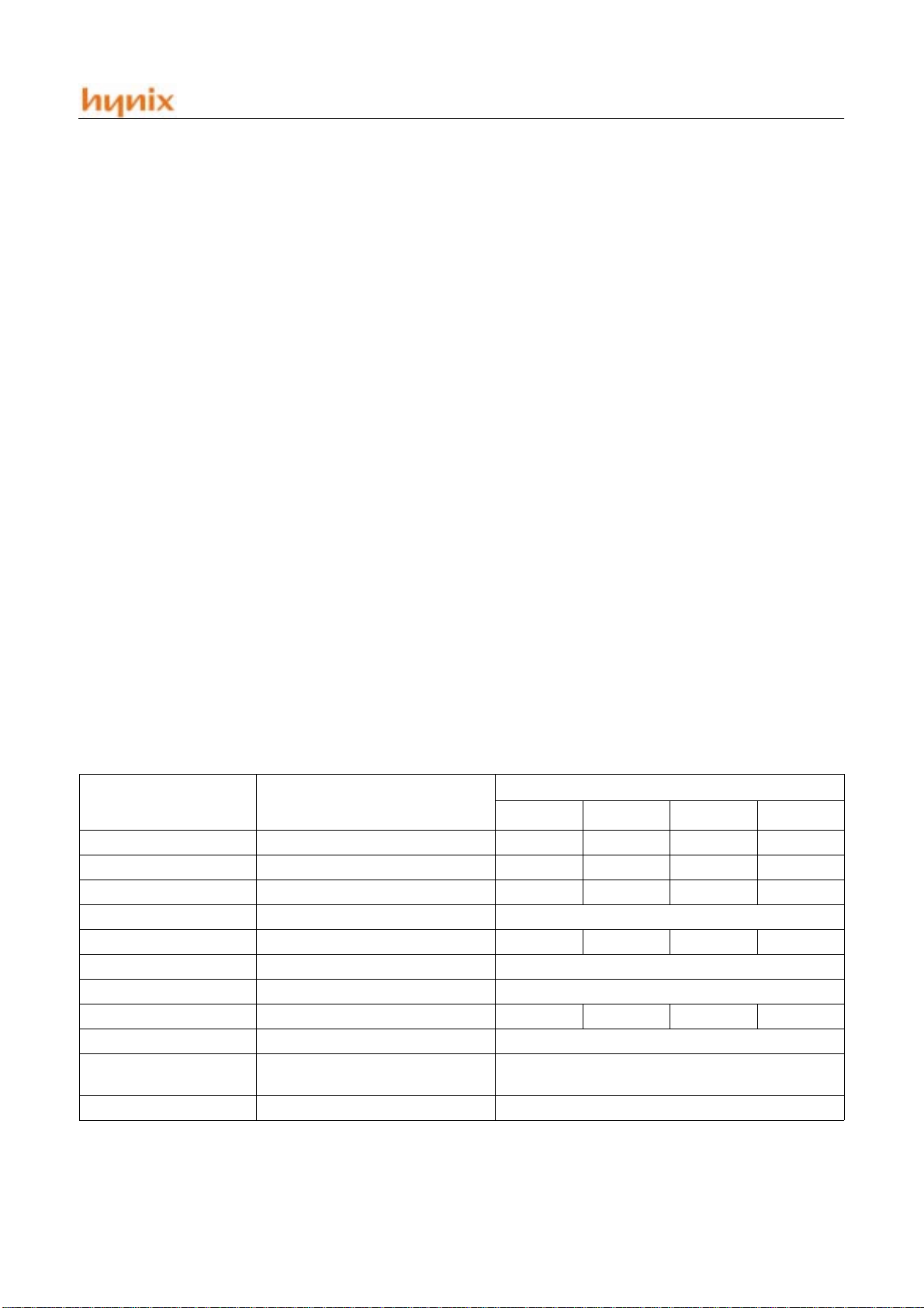
4.2 Special Function Registers
A map of the on -chip memory area called the Specia l Function
Register (SFR) space is shown in Table 4-1 and Table 4-2. Note
that in the SFRs not all of the addresses are occupied. Unoc cupied
addresses are not implemented on the chip. Read accesses to
these addresses will in general return random data, and write accesses will have no effect.
HMS91C8032/97C8032
User software should not write 1s to these unimplemented locations, sinc e they ma y be used in other H MS9XC8032 F amily
products to invoke new fe atures. In th at case th e reset or inac tive
values of the new bits will always be 0, and their active values
will be 1.
F8
F0 B PLLMOD PLLDRH PLLDRL IFCMOD IFCDR2 IFCDR1 IFCDR0 F7
E8 IR3 EF
E0 ACC E7
D8
D0 PSW D7
C8 T2CON RCAP2L RCAP2H TL2 TH2 CF
C0
B8 IP P4MOD P5MOD P6MOD P7MOD BF
B0 IE2 IP2 P0MOD P1MOD P2MOD P3MOD B7
A8
A0 S12CON SBUF1 SBUF2 P0CON P1CON P2CON P3CON A7
98 SCON SBUF 9F
90
88 TCO N TMOD TL0 TL1 TH0 TH1 8F
80 SCMOD SP DPL DPH ADCCON ADCDR PLLDEBUG PCON 87
F8
F0 B
E8 P6DATA
E0 ACC
D8
D0 PSW
C8
C0
B8 P3DATA
B0
A8 P2DATA
A0
98 P1DATA
90
88 P0DATA
80
WDTCON WDTDR RDPG WRPG SFRPG FF
IR2 IT2 DF
IE3 IP3 C7
IE P4CON P5CON P6CON P7CON AF
T34CON T34MOD TL3 TL4 TH3 TH4 97
Table 4-1 SFRPG0 SFR Memory Map (8 Bytes)
Bit Addressable
P7DATA
: in this area, the registers of SFRPG0 are the sam e regi sters of SFRPG1
P5DATA
: in this area, the registers of SFRPG0 are different from registers of SFRPG1
P4DATA
Table 4-2 SFRPG1 SFR Memory Map (8 Bytes)
NOV., 2001 Ver 1.02 19
Page 23

HMS91C8032/97C8032
(MSB)
CY AC F0 RS1 RS0 OV - P
Symbol
CY
AC
F0
RS1
RS0
OV
-
P
NOTE: The contents of (RS1, RS0) enable the working register bank as follows:
Position
PSW.7
PSW.6
PSW.5
PSW.4
PSW.3
PSW.2
PSW.1
PSW.0
(0,0) - Bank 0 (00H-07H)
(0,1) - Bank 1 (08H-0FH)
(1,0) - Bank 2 (10H-17H)
(1,1) - Bank 3 (18H-1FH)
Name and Significance
Carry Flag.
Auxiliary Catrry flag. (For BCD Operations.)
Flag 0. (Available to the user for general purposes.)
Register bank select control bit 1.
Set/clear by software to determine working register bank. (See Note.)
Register bank select control bit 0.
Set/clear by software to determine working register bank. (See Note.)
Overflow flag.
User-definable flag.
Parity flag.
Set/cleared by hardware each instruction cycle to indicate an odd/even
number of "one" bits in the Accumulator, i.e., even parity.
Figure 4-3 Program Status Word (PSW) Register
(LSB)
Accumulator
ACC is the Accumulator register. The mnemonics for accumula-
tor-specific instructions, however, refer to the accumulator simply as A.
B Register
The B register is u s e d d uring multiply and divide operati on s . Fo r
other instructions it can be treated as ano ther scratch pad registe r.
Program Status Word
The PSW register contains program status information as detailed
in Figure 4-3.
Stack Pointer
The Stack Pointer register is 8 bi ts wide . It is in c re mente d b e fore
data is stored during PUSH and CALL executions. While the
stack may reside anywhere in on-chip RAM, the Stack Pointer is
initialized to 07H after a reset. This causes the stack to begin at
locations 08H.
But, it is forbidden to use th e area of 00H to
7FH as the Stack. Thus the stack pointer should be set to the
address larger than 7FH when it is initialized.
Data Pointer
The Data Pointer (DPTR) consists of a high byte (DPH) and a low
byte (DPL). Its intended function is to hold a 16-bit address. It
may be manipulated as a 16-bit register or as two independent
8-bit registers.
Serial Data Buffer
SBUF, SBUF1 and SBUF2 are Serial Buffers. SBUF register is
used by UART, SBUF1 used by SIO1 and SBUF2 used by SIO2.
The SBUF is actually two se parate registers, a transmit buffer a nd
a receive buffer. When data is moved to SBUF, it goes to the
transmit buffer and is held for serial transmission. (Moving a byte
to SBUF is what initiates the transmission.) When data is moved
from SBUF, it comes from the receive buffer.
Unlike SBUF, SBUF1(SBUF2) is one register. If the SIO1(SIO2)
run flag is activated, receive and transmit of serial data is done simultaneously using SBUF1(SBUF2).
Timer Registers Basic to HMS9XC8032
Register pairs (THx, TLx) are the 16-bit Counting regis ters for
Timer/Counters 0, 1, 2, 3 and 4, respectively.
Control Register for the HMS9XC8032
Special Functio n Regist ers IP x, IEx, TMOD, T 34MOD, TCO N,
T2CON, SCON, S12CON, PCON and etc. contain control and
status bits for the various peripherals in HMS9XC8032. They are
described in later sections.
20 NOV., 2001 Ver 1.02
Page 24
HMS91C8032/97C8032
Summary of SFR
PSW: PROGRAM STATUS WORD. BIT ADDRESSABLE. : D0H
CY AC F0 RS1 RS0 OV - P
CY PSW.7 Carry Flag.
AC PSW.6 Auxiliary Carry Flag.
F0 PSW.5 Flag 0 available to the user for ge neral purpose.
RS1 PSW.4 Register Bank selector bit 1 (See NOTE 1).
RS0 PSW.3 Register Bank selector bit 0 (See NOTE 1).
OV PSW.2 Overflow Flag.
- PSW.1 User flag.
P PSW.0 Parity flag. Set/cleared by hardware each instruction cycle to indicate an odd/even number of ‘1’ bits in
th accumulator.
NOTE 1:
The value presented by RS0 and RS1 selects the corresponding register bank.
RS1 RS0 Register Bank Addresss
0 0 0 00H-07H
01 1 08H-0FH
1 0 2 10H-17H
11 3 18H-1FH
PCON: POWER CONTROL REGISTER. NOT BIT ADDRESSABLE. : 87H
SMOD - - - GF1 GF0 PD IDL
SMOD PCON.7 Double baud rate bit. If Timer 1 is used to generate baud rate and SMOD = 1, th e baud rate is doubled
when the Serial Port is used in modes 1, 2, or 3.
- PCON.6 Not implemented, reserved for future use.*
- PCON.5 Not implemented, reserved for future use.*
- PCON.4 Not implemented, reserved for future use.*
GF1 PCON.3 General pu rpose flag bit.
GF0 PCON.2 General pu rpose flag bit.
PD PCON.1 Power Down bit. Setting this bit activates Power Down operation.
IDL PCON.0 dle Mode bit. Setting this bit activates Idle Mode operation.
If 1s are written to PD and IDL at the same time, PD takes precedence.
*User software should not write 1s to reserved bits. These bits may be used in future DTS3 products to invoke new features. In that case,
the reset or inactive value of the new bit will be 0, and its active value will be 1.
NOV., 2001 Ver 1.02 21
Page 25
HMS91C8032/97C8032
INTERRUPTS:
In order to use any of the interrupt in the DTS3, the following three steps must be taken.
1. Set the EA (Enable All) bit in the IE Register to 1.
2. Set the corresponding individual interrupt enable bit in the IE, IE2 and IE3 regi ster to 1.
3. Begin the interrupt service routine at the corresponding Vector Address of that interrupt. See Table below.
Interrupt
Source
INTEX0 0003H
INTT0 000BH
INTEX1 0013H
INTT1 001BH
INTS0 (RI & TI) 0023H
INTT2 (TF2 & EXF2) 002BH
INTWDT 0033H
INTIFC 003BH
INTAD 0043H
INTEX2 004BH
INTEX3 0053H
INTEX4 005BH
INTS1 0063H
INTS2 006BH
INTEX5 0073H
INTEX6 007BH
INTT3 0083H
INTT4 008BH
Vector
Address
Table 4-3 Intrrupt Vector
IE: INTERRUPT ENABLE REGISTER. BIT ADDRESSABLE. : A8H
If the bit is 0, the corresponding interrupt is disabled. If the bit is 1, the corresponding interrupt is enabled.
EA - IET2 IES0 IET1 IEX1 IET0 IEX0
EA IE.7 Disables all interrupt. If EA = 0. no interrupt will be acknowledged. IF EA = 1, each interrupt source is
individually enabled or disabled by setting or clearing its enable bit.
- IE.6 Not implemented, reserved for future use.*
IET2 IE.5 Enable or disable the Timer 2 overflow or capture interrupt
IES0 IE.4 Enable or disable the serial port interrupt.
IET1 IE.3 Enable or disable the Timer 1 overflow interrupt.
IEX1 IE.2 Enable or disable External Interrupt 1
IET0 IE.1 Enable or disable the Timer 0 overflow interrupt.
IEX0 IE.0 Enable or disable External Interrupt 0.
* User software should not write 1s to reserved bits. These bits may be used in future DTS3 products to invo ke new features. In that case,
the reset or inactive value of the new bit will be 0, and its active value will be 1.
22 NOV., 2001 Ver 1.02
Page 26

HMS91C8032/97C8032
IE2: INTERRUPT ENABLE REGISTER 2. BIT ADDRESSABLE. : B0H
If the bit is 0, the corresponding interrupt is disabled. If the bit is 1, the corresponding interrupt is enabled.
- - - IEX6 IEX5 IEX4 IEX3 IEX2
- IE2.7 Not implemented, reserved for future use.*
- IE2.6 Not implemented, reserved for future use.*
- IE2.5 Not implemented, reserved for future use.*
IEX6 IE 2.4 Enable or disable External Interrupt 6
IEX5 IE 2.3 Enable or disable External Interrupt 5
IEX4 IE 2.2 Enable or disable External Interrupt 4
IEX3 IE 2.1 Enable or disable External Interrupt 3
IEX2 IE 2.0 Enable or disable External Interrupt 2.
* User software should not write 1s to reserved bits. These bits may be used in future DTS3 products to invo ke new features. In that case,
the reset or inactive value of the new bit will be 0, and its active value will be 1.
IE3: INTERRUPT ENABLE REGISTER 3. BIT ADDRESSABLE. : C0H
If the bit is 0, the corresponding interrupt is disabled. If the bit is 1, the corresponding interrupt is enabled.
- IEWDT IEADC IEIF IES2 IES1 IET4 IET3
- IE3.7 Not implemented, reserved for future use.*
IEWDT IE3.5 Enable or disable Watchdog timer interrupt
IEADC IE3.6 Enable or disable A/D conversion completion interrupt
IEIF IE3.4 Enable or disable IF counter interrupt
IES2 IE3.3 Enable or disable SIO2 interrupt
IES1 IE3.2 Enable or disable SIO1 Interrupt
IET4 IE3.1 Enable or disable the Timer 4 overflow interrupt.
IET3 IE3.0 Enable or disable the Timer 3 overflow interrupt.
* User software should not write 1s to reserved bits. These bits may be used in future DTS3 products to invo ke new features. In that case,
the reset or inactive value of the new bit will be 0, and its active value will be 1.
ASSIGNING HIGHER PRIORITY TO ONE OR MORE INTERRUPTS:
In order to assign higher priority to an interrupt the corresponding bit in the IP0, IP1 and IP2 register must be set to 1.
Remember that while an interrupt service is progress, it cannot be interrupted by a lower or same level interrupt.
PRIORITY WITHIN LEVEL:
Priority within level is only to resolve simultaneous requests of the same priority level.
From high to low, interrupt sources are listed below:
INTEX0
INTT0
INTEX1
INTT1
NOV., 2001 Ver 1.02 23
Page 27

HMS91C8032/97C8032
INTS0 (RI or TI)
INTT2 (TF2 or EXF2)
INTWDT
INTIFC
INTAD
INTEX2
INTEX3
INTEX4
INTS1
INTS2
INTEX5
INTEX6
INTT3
INTT4
IP: INTERRUPT PRIORITY REGISTER. BIT ADDRESSABLE. : B8H
If the bit is 0, the corresponding interrupt has a lower priority and If the bit is 1, the corresponding interrupt has a higher priority.
- - IPT2 IPS0 IPT1 IPX1 IPT0 IPX0
- IP.7 Not implemented, reserved for future use.*
- IP.6 Not implemented, reserved for future use.*
IPT2 IP.5 Defines the Timer 2 interrupt priority level
IPS IP.4 Defines the Serial Port interrupt priority level.
IPT1 IP.3 Defines the Timer 1 interrupt priority level.
IPX1 IP.2 Defines External Interrupt 1 priority level.
IPT0 IP.1 Defines the Timer 0 interrupt priority level.
IPX0 IP.0 Defines the External Interrupt 0 priority level.
* User software should not write 1s to reserved bits. These bits may be used in future DTS3 products to invo ke new features. In that case,
the reset or inactive value of the new bit will be 0, and its active value will be 1.
IP2: INTERRUPT PRIORITY REGISTER 2. : B1H
If the bit is 0, the corresponding interrupt has a lower priority and If the bit is 1, the corresponding interrupt has a higher priority.
- - - IPX6 IPX5 IPX4 IPX3 IPX2
- IP2.7 Not implemented, reserved for future use.*
- IP2.6 Not implemented, reserved for future use.*
- IP2.5 Not implemented, reserved for future use.*
IPX6 IP2.4 Defines External Interrupt 6 priority level.
IPX5 IP2.3 Defines External Interrupt 5 priority level.
IPX4 IP2.2 Defines External Interrupt 4 priority level.
IPX3 IP2.1 Defines External Interrupt 3 priority level.
IPX2 IP2.0 Defines External Interrupt 2 priority level.
* User software should not write 1s to reserved bits. These bits may be used in future DTS3 products to invo ke new features. In that case,
the reset or inactive value of the new bit will be 0, and its active value will be 1.
24 NOV., 2001 Ver 1.02
Page 28

HMS91C8032/97C8032
IP3: INTERRUPT PRIORITY REGISTER 3. : C1H
If the bit is 0, the corresponding interrupt has a lower priority and If the bit is 1, the corresponding interrupt has a higher priority.
- IPWDT IPADC IPIFC IPS2 IPS1 IPT4 IPT3
- IP3.7 Not implemented, reserved for future use.*
IPWDT IP3.6 Defines the Watchdog timer interrupt priority level.
IPADC IP3.5 Defines ADC interrupt priority level.
IPIFC IP3.4 Defines IF counter interrupt priority level.
IPS2 IP3.3 Defines SIO2 interrupt priority level.
IPS1 IP3.2 Defines SIO1 Interrupt priority level.
IPT4 IP3.1 Defines the Timer 4 interrupt priority level.
IPT3 IP3.0 Defines the Timer 3 interrupt priority level.
* User software should not write 1s to reserved bits. These bits may be used in future DTS3 products to invo ke new features. In that case,
the reset or inactive value of the new bit will be 0, and its active value will be 1.
REQUESTING TO SERVICE ONE OR MORE INTERRUPTS:
IR2: INTERRUPT REQUEST REGISTER 2. BIT ADDRESSABLE. : D8H
- - - IRX6 IRX5 IRX4 IRX3 IRX2
- IR2.7 Reserved for future use *
- IR2.6 Reserved for future use *
- IR2.5 Reserved for future use *
IRX6 IR2.4 External interrupt 6 flag. Set by hardware when External interrupt is detected. Cleared by hardware
when interrupt is processed.
IRX5 IR2.3 External interrupt 5 flag. Set by hardware when External interrupt is detected. Cleared by hardware
when interrupt is processed.
IRX4 IR2.2 External interrupt 4 flag. Set by hardware when External interrupt is detected. Cleared by hardware
when interrupt is processed.
IRX3 IR2.1 External interrupt 3 flag. Set by hardware when External interrupt is detected. Cleared by hardware
when interrupt is processed.
IRX2 IR2.0 External interrupt 2 flag. Set by hardware when External interrupt is detected. Cleared by hardware
when interrupt is processed.
* User software should not write 1s to reserved bits. These bits may be used in future DTS3 products to invo ke new features. In that case,
the reset or inactive value of the new bit will be 0, and its active value will be 1.
IR3: INTERRUPT REQUEST REGISTER 3. BIT ADDRESSABLE. : E8H
- IRWDT IRADC IRIFC IRS2 IRS1 IRT4 IRT3
- IR3.7 Reserved for future use *
IRWDT IR3.6 Watchdog timer overflow flag. Set by hardware when WDT overflows. Cleared by hardware as proces-
sor vectors to the interrupt service routine.
IRADC IR3.5 A/D conversion completio n flag. Set by hard ware when ADC completes. Cleared by hardware as pro-
cessor vectors to the interrupt service routine.
IRIFC IR3.4 IF counter interrupt flag. Set by hardware when run time of IF counter reaches to gate time. Cleared by
hardware as processor vectors to the interrupt service routine.
IRS2 IR3.3 SIO2 interrupt flag. Set by hardware when one TX/RX is completed. Cleared by hardware as processor
NOV., 2001 Ver 1.02 25
Page 29
HMS91C8032/97C8032
vectors to the interrupt service routine.
IRS1 IR3.2 SIO1 interrupt flag. Set by hardware when one TX/RX is completed. Cleared by hardware when inter-
rupt is processed.
IRT4 IR3.1 Timer 4 Overflow flag. Set by hardware when the Timer/Counter 4 overflows. Cleared by hardware as
processor vectors to the interrupt service routine.
IRT3 IR3.0 Timer 3 Overflow flag. Set by hardware when the Timer/Counter 3 overflows. Cleared by hardware as
processor vectors to the interrupt service routine.
* User software should not write 1s to reserved bits. These bits may be used in future DTS3 products to invo ke new features. In that case,
the reset or inactive value of the new bit will be 0, and its active value will be 1.
IT2: EXTERNAL INTERRUPT TPYE REGISTER 2. BIT ADDRESSABLE. : D9H
IT5M1 IT5M0 IT4M1 IT4M0 IT3M1 IT3M0 IT2M1 IT2M0
IT5M1 IT2.7 See Table 4-4
IT5M0 IT2.6 See Table 4-4
IT4M1 IT2.5 See Table 4-4
IT4M0 IT2.4 See Table 4-4
IT3M1 IT2.3 See Table 4-4
IT3M0 IT2.2 See Table 4-4
IT2M1 IT2.1 See Table 4-4
IT2M0 IT2.0 See Table 4-4
ITxM[1:0] Select interrupt detect mode
0 0 Both rising & falling edge detection
0 1 Rising edge detect mode
1 0 Falling edge detect mode
1 1 Level (high) detect mode
Table 4-4 Interrupt Detect Mode
TCON: TIMER01/COUNTER01 CONTROL REGISTER. BIT ADDRESSABLE. : 88H
TF1 TR1 TF0 TR0 IE1 IT1 IE0 IT0
TF1 TCON.7 Timer 1 Overflow flag. Set by hardware when the Timer/Counter 1 overflows. Cleared by hardware as
processor vectors to the interrupt service routine.
TR1 TCON.6 Timer 1 run control bit. Set/cleared by software to turn Timer/Counter 1 ON/OFF.
TF0 TCON.5 Timer 0 Overflow flag. Set by hardware when the Timer/Counter 0 overflows. Cleared by hardware as
processor vectors to the interrupt service routine.
TR0 TCON.4 Timer 0 run control bit. Set/cleared by software to turn Timer/Counter 0 ON/OFF.
IE1 TCON.3 Interrupt 1 Edge flag. Set by hardware when external interrupt edge detected. Cleared when interrupt
processed.
IT1 TCON.2 Interrupt 1 Type control bit. Set/cleared by software to specify falling edge/low level triggered external
interrupts.
IE0 TCON.1 Interrupt 0 Edge flag. Set by hardware when external interrupt edge detected. Cleared when interrupt
processed.
IT0 TCON.0 Interrupt 0 Type control bit. Set/cleared by software to specify falling edge/low level triggered external
interrupts.
26 NOV., 2001 Ver 1.02
Page 30
HMS91C8032/97C8032
T34CON: TIMER34/COUNTER34 CONTROL REGISTER. BIT ADDRESSABLE. : 90H
TF4 TR4 TF3 TR3 T3_SUB T4_SUB
TF4 TCON.7 Timer 4 Overflow flag. Set by hardware when the Timer/Counter 4 overflows. Cleared by hardware as
processor vectors to the interrupt service routine.
TR4 TCON.6 Timer 4 run control bit. Set/cleared by software to turn Timer/Counter 4 ON/OFF.
TF3 TCON.5 Timer 3 Overflow flag. Set by hardware when the Timer/Counter 3 overflows. Cleared by hardware as
processor vectors to the interrupt service routine.
TR3 TCON.4 Timer 3 run control bit. Set/cleared by software to turn Timer/Counter 3 ON/OFF.
- TCON.3 Reserved for future use *
T3_SUB TCON.2 Switch main clock to sub clock for timer3 counting. This bit is a write-only register.
0 = Main Osc, 1 = Sub Osc.
- TCON.1 Reserved for future use *
T4_SUB TCON.0 Switch main clock to sub clock for timer4 counting. This bit is a write-only register.
0 = Main Osc, 1 = Sub Osc.
* User software should not write 1s to reserved bits. These bits may be used in future DTS3 products to invo ke new features. In that case,
the reset or inactive value of the new bit will be 0, and its active value will be 1.
TMOD: TIMER/COUNTER MODE CONTROL REGISTER. NOT BIT ADDRESSABLE. : 89H
GATE C /T M1 M0 GATE C/T M1 M0
Timer 1
GATE TMOD.7 When TRx (in TCON) is set and GATE = 1, TIMER/COUNTERx will run only while INTx pin is high
(hardware control). When GATE = 0, TIMER/COUNTERx will run only while TRx = 1 (software con-
trol).
C/T TMOD.6 Timer or Counter selector. Cleared for Timer operation (input from internal system clock). Set for
Counter operation (input from Tx input pin).
M1 TMOD.5 Mode selector bit. (See Table 4-5)
M0 TMOD.4 Mode selector bit. (See Table 4-5)
GATE TMOD.3 When TRx (in TCON) is set and GATE = 1, TIMER/COUNTERx will run only while INTx pin is high
(hardware control). When GATE = 0, TIMER/COUNTERx will run only while TRx = 1 (software con-
trol).
C/T TMOD.2 Timer or Counter selector. Cleared for Timer operation (input from internal system clock). Set for
Counter operation (input from Tx input pin).
M1 TMOD.1 Mode selector bit. (See Table 4-5)
M0 TMOD.0 Mode selector bit. (See Table 4-5)
M1 M0 Mode Operating Mode
0 0 0 13-bit Timer
0 1 1 16-bit Timer/Counter
1 0 2 8-bit Auto-Reload Timer/Counter
113
1 1 3 (Timer 1) Timer/Counter 1 stopped.
(Timer 0) TL0 is an 8-bit Timer/Counter controlled by the standard Timer 0
control bits, TH0 is an 8-bit Timer and is controlled by Timer 1 control bits.
Timer 0
Table 4-5 Timer 0 and Timer 1 Mode
NOV., 2001 Ver 1.02 27
Page 31

HMS91C8032/97C8032
T34MOD: TIMER/COUNTER MODE CONTROL REGISTER. NOT BIT ADDRESSABLE. : 91H
GATE C/T M1 M0 GATE C/T M1 M0
Timer 4
GATE T34MOD.7 When TRx (in TCON) is set and GATE = 1, TIMER/COUNTERx will run only while INTx pin is high
(hardware control). When GATE = 0, TIMER/COUNTERx will run only while TRx = 1 (software con-
trol).
C/T T34MOD.6 Timer or Counter selector. Cleared for Timer operation (input from internal system clock). Set for
Counter operation (input from Tx input pin).
M1 T34MOD.5 Mode selector bit. (See Table 4-6)
M0 T34MOD.4 Mode selector bit. (See Table 4-6)
GATE T34MOD.3 When TRx (in TCON) is set and GATE = 1, TIMER/COUNTERx will run only while INTx pin is high
(hardware control). When GATE = 0, TIMER/COUNTERx will run only while TRx = 1 (software con-
trol).
C/T T34MOD.2 Timer or Counter selector. Cleared for Timer operation (input from internal system clock). Set for
Counter operation (input from Tx input pin).
M1 T34MOD.1 Mode selector bit. (See Table 4-6)
M0 T34MOD.0 Mode selector bit. (See Table 4-6)
Timer 3
M1 M0 Mode Operating Mode
0 0 0 13-bit Timer
0 1 1 16-bit Timer/Counter
1 0 2 8-bit Auto-Reload Timer/Counter
113
1 1 3 (Timer 4) Timer/Counter 4 stopped.
(Timer 3) TL3 is an 8-b it Tim er/Counte r controll ed by the sta ndard T imer 3 control bits, TH3 is an 8-bit Timer and is controlled by Timer 4 control bits.
Table 4-6 Timer 3 and Timer 4 Mode
TIMER SET-UP
TIMER/COUNTER 0 (TIMER/COUNTER 3)
TMOD (T34MOD)
MODE
0 13-bit Timer 00H 08H
1 16-bit Timer 01H 09H
2 8-bit Auto-Reload 02H 0AH
3 two 8-bit Timers 03H 0BH
TIMER 0 (TIMER 3)
FUNTION
INTERNAL
CONTROL
(NOTE 1) (NOTE 2)
EXTERNAL
CONTROL
Table 4-7 Timer0 and Timer3 TMOD
28 NOV., 2001 Ver 1.02
Page 32

TMOD (T34MOD)
HMS91C8032/97C8032
MODE
0 13-bit Timer 04H 0CH
1 16-bit Timer 05H 0DH
2 8-bit Auto-Reload 06H 0EH
3 One 8-bit Counter 07H 0FH
NOTES:
1. The Timer is turned ON/OFF by setting/clearing bit TR0 (TR3) by the software.
2. The Timer is turned ON/OFF by the 1 to 0 transition on /INT0 (/INT3) when TR0 = 1 (hardware control).
COUNTER 0 (COUNTER 3)
FUNTION
Table 4-8 Counter0 and Counter3 TMOD
INTERNAL
CONTROL
(NOTE 1) (NOTE 2)
EXTERNAL
CONTROL
TIMER/COUNTER 1 (TIMER/COUNTER 4)
TMOD (T34MOD)
MODE
0 13-bit Timer 00H 80H
1 16-bit Timer 10H 90H
2 8-bit Auto-Reload 20H A0H
3 does not run 30H B0H
TIMER 1 (TIMER 4)
FUNTION
INTERNAL
CONTROL
(NOTE 1) (NOTE 2)
EXTERNAL
CONTROL
Table 4-9 Timer0 and Timer3 TMOD
TMOD (T34MOD)
MODE
0 13-bit Timer 40H C0H
1 16-bit Timer 50H D0H
2 8-bit Auto-Reload 60H E0H
3 not available - -
NOTES:
1. The Timer is turned ON/OFF by setting/clearing bit TR0 (TR3) by the software.
2. The Timer is turned ON/OFF by the 1 to 0 transition on /INT1 (/INT4) when TR1 = 1 (hardware control).
COUNTER 1 (COUNTER 4)
FUNTION
Table 4-10 Counter0 and Counter3 TMOD
INTERNAL
CONTROL
(NOTE 1) (NOTE 2)
EXTERNAL
CONTROL
NOV., 2001 Ver 1.02 29
Page 33

HMS91C8032/97C8032
T2CON: TIMER/COUNTER 2 CONTROL REGISTER. BIT ADDRESSABLE. : C8H
TF2 EXF2 RCLK TCLK EXEN2 TR2 C/T2
TF2 T2CON.7 Timer 2 Overflow flag set by hardware and cleared by software. TF2 cannot be set when either RCLK
=1 or TCLK = 1.
EXF2 T2CON.6 Timer 2 external flag set when e ither a captur e or reloa d is cau sed by a n egativ e transition on T2 EX, and
EXEN2 = 1. When Timer 2 interrupt is enabled, EXF2 = 1 will cause the CPU to vector to the Timer 2
interrupt routine. EXF2 must be cleared by software.
RCLK T2CON.5 Receive clock flag. When set, causes the Serial Port to use Timer 2 overflow pulses for its receive clock
in modes 1 & 3. RCLK = 0 causes Timer 1 overflow to be used for the receive c lock.
TCLK T2CON.4 Transmit clock flag. When set, causes the Serial Port to use Timer 2 overflow pulses for its transmit
clock in modes 1 & 3. TCLK = 0 causes Timer 1 overflow to be used for the transmit clock.
EXEN2 T2CON.3 Timer 2 external enable flag. When set, allows a capture or reload to occur as a result of negative transi-
tion on T2EX if Timer 2 is not being used to clock the Serial Port.
EXEN2 = 0 causes Timer 2 to ignore events at T2EX.
TR2 T2CON.2 Software START/STOP control for Timer 2 . A logic 1 starts the Timer.
C/T2
CP/RL2
T2CON.1 Timer or Counter selector.
0 = Internal Timer
1 = External Event Counter (falling edge trigge red) .
T2CON.0 Capture/Reload flag. When set, captures will occur on negative transitions at T2EX if EXEN2 = 1.
When cleared, Auto-Reloads will occur either with Timer 2 overflows or negative transitions at T2EX
when EXEN2 =1. When either RCLK = 1 or TCLK = 1, this bit is ignored and the Timer is forced to
Auto-Reload on Timer 2 overflow.
CP/RL2
TIMER/COUNTER 2 SET-UP
Except for the baud rate generato r mode, the value given for T2C ON do not inc lude the settin g of the TR2 bi t. Therefore , bit TR2 mu s t be
set, separately, to turn the Timer on.
T2CON
MODE
16-bit Auto-Reload 00H 08H
16-bit Capture 01H 09H
BAUD rate generator receive & transmit
same baud rate
receive only 24H 26H
transmit only 14H 16H
Table 4-11 Timer 2 Mode
INTERNAL
CONTROL
(NOTE 1) (NOTE 2)
34H 36H
EXTERNAL
CONTROL
30 NOV., 2001 Ver 1.02
Page 34

TMOD
HMS91C8032/97C8032
MODE
INTERNAL
CONTROL
EXTERNAL
CONTROL
(NOTE 1) (NOTE 2)
16-bit Auto-Reload 02H 0AH
16-bit Capture 03H 0BH
Table 4-12 Counter 2 Mode
NOTES:
1. Capture/Reload occurs only on Timer/Counter overflow.
2. Capture/Reload occurs on Timer/Counter overflow and a 1 to 0 transition on T2EX pin except when Timer 2 is used in the baud rate
generating mode.
SCON: SERIAL PORT CONTROL REGISTER.(UART) BIT ADDRESSABLE. : 98H
SM0 SM1 SM2 REN TB8 RB8 TI RI
SM0 SCON.7 Serial Port mode specifier. (See Table 4-13).
SM1 SCON.6 Serial Port mode specifier. (See Table 4-13).
SM2 SCON.5 Enables the multiprocessor communication feature in modes 2&3. In modes 2 or 3, if SM2 is set to 1
then RI will not be activated if the received 9th data bit (RB8) is 0. In mode 1, if SM2 = 1 then RI will
not be activated if a valid stop bit was not received. In mode 0, SM2 should be 0.
REN SCON.4 Set/C le ared by software to Enable/Disable reception.
TB8 S CON.3 The 9th bit that will be transmitted in modes 2 & 3. Set/Cleared by software.
RB8 SCON.2 In modes 2 & 3, is the 9th data bit that was received. In mode 1, if SM2 = 0, RB8 is the stop bit that was
received, In mode 0, RB8 is not used.
TI SCON.1 Transmit interrupt flag. Set by hardware at the end 8th bit time in mode 0, or at the beginning of the stop
bit in the other modes. Must be cleared by software.
RI SCON.0 Receive interrupt flag. Set by hardware at the end 8th bit time in mode 0, or halfway through the stop bit
in the other modes (except see SM2). Must be clear e d by software.
SM0 SM1 Mode Description Baud Rate
/6*
0 0 0 SHIFT REGISTER
f
CPU
0 1 1 8-Bit UART Variable
1 0 2 9-Bit UART
f
CPU
/32* or f
CPU
/16*
1 1 3 9-Bit UART Variable
Table 4-13 UART Mode
: CPU Clock Frequency (f
* f
CPU
f
: Oscillator Clock Frequency
OSC
OSC
/2, f
OSC
/4, f
OSC
/8, f
OSC
/16, f
OSC
/32)
NOV., 2001 Ver 1.02 31
Page 35

HMS91C8032/97C8032
SERIAL PORT SET-UP
MODE SCON SM2 VARIATION
0
1
2
3
0
1
2
3
10H
50H
90H
D0H
NA
70H
B0H
F0H
Table 4-14 Serial Port
Single Processor
Environment
(SM2 = 0)
Multiprocessor
Environment
(SM2 = 1)
GENERATING BAUD RATES
Serial Port in Mode 0:
Timer/Counters need to be stop. Only the SCON register needs to be defined.
2f
×
CPU
Baud Rate
---------------------
=
12
Serial Port in Mode 1:
Mode 1 has a variable baud rate. The baud rate can be generated by either Timer 1 or Timer 2
USING TIMER/COUNTER 1 TO GENERATE BAUD RATES:
For this purpose, Timer 1 is used in mode 2 (Auto-Reload). Refer to Timer Setup section of this chapter.
K2f
××
Baud Rate
If SMOD = 0, then K =1.
If SMOD = 1, then K = 2. (SMOD is the PCON register).
Most of the timer the user knows the baud rate and needs to know the reload value for TH1.
Therefore, the equation to calculate TH1 can be written as:
TH1 256
TH1 must be an integer value. Rounding off TH1 to the nearest integer may not produce the desired baud rate. In this case, the user may
have to choose another crystal frequenc y.
Since the PCON register is not bit addressable, one way to set the bit is logical ORing the PCON register. (i.e., ORL PCON, #80H). The
address of PCON is 87H.
------------------------------------------------------------
=
32 12×256 TH1
K2f
----------------------------------------
–=
384 Baud Rate
×
CPU
()–[]×
××
CPU
USING TIMER/COUNTER 2 TO GENERATE BAUD RATES:
For this purpose, Timer 2 must be used in the baud rate generating mode. If Timer 2 is being clocked through pin T2 the baud rate is:
Timer2 Overflow Rate
------------------------------------------------------ -
Baud Rate
=
16
32 NOV., 2001 Ver 1.02
Page 36

And if it is being clocked internally the baud rate is:
2f
×
Baud Rate
-------------------------------------------------------------------------------------------------
=
32 65536
CPU
()–[]×
RCAP2H RCAP2L
,
To obtain the reload value for RCAP2H and RCAP2Ll the above can be rewritten as:
2f
×
CPU
RCAP2H, RCAP2L
65535
-------------------------------------
–=
32 Baud Rate
×
SERIAL PORT IN MODE 2:
HMS91C8032/97C8032
The baud rate is fixed in this mode and is 1/
16
or 1/
of the CPU clock depending on the value of the SMOD bit in the PCON register.
32
In this mode, the Timers are used and the clock comes from the internal phase 2 clock.
SMOD = 1
2f
×
CPU
Baud Rate
---------------------
=
32
SMOD = 0
2f
×
CPU
Baud Rate
---------------------
=
64
To set the SMOD bit: ORL PCON, #80H. The address of PCON is 87H.
SERIAL PORT IN MODE 3:
The baud rate in mode 3 is variable and sets up exactly the same as in mode 1.
S12CON: SIO1 & SIO2 CONTROL REGISTER. BIT ADDRESSABLE. : A0H
SIO2HIZ SIO2TS SIO2CK1 SIO2CK0 SIO1HIZ SIO1TS SIO1CK1 SIO1CK0
SIO2HIZ S12CON.7 Software Port control for SiO2. A logic 1 assigns general I/O port to SIO2 port
SIO2TS S12CON.6 Software START/STOP control for SIO2. A logic 1 starts the SIO2
SIO2CK1 S12CON.5 See Table 4-15
SIO2CK0 S12CON.4 See Table 4-15
SIO1HIZ S12CON.3 Software Port control for SiO1. A logic 1 assigns general I/O port to SIO1 port
SIO1TS S12CON.2 Software START/STOP control for SIO1. A logic 1 starts the SIO1
SIO1CK1 S12CON.1 See Table 4-15
SIO1CK0 S12CON.0 See Table 4-15
:
SIO1/2CK1 SIO1/2CK0
Set input/output clock frequency of SIO1 (f
= 7.2 MHz)
OSC
0 0 Slave mode : External clock
0 1 Master mode : 75KHz
1 0 Master mode : 150KHz
1 1 Master mode : 450KHz
Table 4-15 SIO Clock
NOV., 2001 Ver 1.02 33
Page 37

HMS91C8032/97C8032
PLLMOD : PLL MODE & REFERENCE FREQUENCY SELECT REGISTER. BIT ADDRESSABLE. : F1H
PLLRF3 PLLRF2 PLLRF1 PLLRF0 PLLUL1 PLLUL0 PLLMD1 PLLMD0
PLLRF3 PLLMOD.7 See Table 4-16
PLLRF2 PLLMOD.6 See Table 4-16
PLLRF1 PLLMOD.5 See Table 4-16
PLLRF0 PLLMOD.4 See Table 4-16
PLLUL1 PLLMOD.3
PLLUL0 PLLMOD.2
PLLMD1 PLLMOD.1 See Table 4-17
PLLMD0 PLLMOD.0 See Table 4-17
Detects status of unlock FF1 (1.1µs). Set by hardware when PLL locks 900KHz
Detects status of unlock FF0 (2.2µs). Set by hardware when PLL locks 450KHz
PLLRF3 PLLRF2 PLLRF1 PLLRF0
0000PLL stop
00011KHz
00101.25KHz
00112.5KHz
01003KHz
01015KHz
01106.25KHz
01119KHz
100010KHz
100112.5KHz
101018KHz
101120KHz
110025KHz
110150KHz
1110Reserved for future use *
1111Reserved for future use *
Table 4-16 PLL Reference Frequency
Reference Frequency of PLL (f
= 7.2 MHz)
OSC
* User software should not write 1s to reserved bits. These bits may be used in future DTS3 products to invo ke new features. In that case,
the reset or inactive value of the new bit will be 0, and its active value will be 1.
PLLMD1 PLLMD0
0 0 Disable VCOL & VCOH pins
0 1 VCOH & VHF mode select
1 0 VCOL & HF mode select
1 1 VCOL & MF mode select
Selects of PLL input pin (f
Table 4-17 PLL Mode
= 7.2 MHz)
OSC
34 NOV., 2001 Ver 1.02
Page 38

HMS91C8032/97C8032
IFCMOD : IFC MODE SELECT & CONTROL REGISTER. BIT ADDRESSABLE. : F4H
IFCJR IFCST IFCCLR - IFCGT1 IFCGT0 IFCMD1 IFCMD0
IFCJR IFCMOD.7 IF counter judge register. Set by hardware automatically when IF counting is ended, Cleared by hard-
ware automatically when software reads IFCMOD register or IF interrupt service routine is started.
IFCST IFCMOD.6 Software START/STOP control for IF counter. A logic 1 starts the IF counter.
IFCCLR IFCMOD.5 A logic 1 resets the IF counter.
IFCMOD.4 Reserved for future use *
IFCGT1 IFCMOD.3 See Table 4-18
IFCGT0 IFCMOD.2 See Table 4-18
IFCMD1 IFCMOD.1 See Table 4-19
IFCMD0 IFCMOD.0 See Table 4-19
NOTE:
IFCGT1
008ms
0132ms
1 0 128ms
11Soft
IFCMD1 IFCMD0 Selects of IFC input
0 X Disable FMIFC & AMIFC pins
10FMIFC pin select
1 1 AMIFC pin select
* User software should not write 1s to reserved bits. These bits may be used in future DTS3 products to invo ke new features. In that case,
the reset or inactive value of the new bit will be 0, and its active value will be 1.
IFCGT0 Setting of IFC gate time (f
Table 4-18 IFC Gate Time
Table 4-19 IFC Mode
= 7.2 MHz)
OSC
NOV., 2001 Ver 1.02 35
Page 39

HMS91C8032/97C8032
IFCDR2 : IF counter data register 2. : F5H
----IFCDETIFCDATA18IFCDATA17IFCDATA16
- IFCDR2.7 Reserved for future use
- IFCDR2.6 Reserved for future use
- IFCDR2.5 Reserved for future use
- IFCDR2.4 Reserved for future use
IFCDET IFCDR2.3 Detection bit of 19bit IF counter overflow. A logic 1 implies the overflow of IF counter. It can
be reset by IFCCLR. (See IF Counter Control Register
IFCDATA18 IFCDR2.2
IFCDATA17 IFCDR2.1
IFCDATA16 IFCDR2.0
IFCDR1 : IF counter data register 1. : F6H
IFCDATA15 IFCDATA14 IFCDATA13 IFCDATA12 IFCDATA11 IFCDATA10 IFCDATA9 IFCDATA8
th
19
bit of 19bit IF counter (MSB)
18th bit of 19bit IF counter
17th bit of 19bit IF counter
IFCDATA15 IFCDR1.7
IFCDATA14 IFCDR1.6
IFCDATA13 IFCDR1.5
IFCDATA12 IFCDR1.4
IFCDATA11 IFCDR1.3
IFCDATA10 IFCDR1.2
IFCDATA9 IFCDR1.1
IFCDATA8 IFCDR1.0
th
16
bit of 19bit IF counter
15th bit of 19bit IF counter
14th bit of 19bit IF counter
13th bit of 19bit IF counter
12th bit of 19bit IF counter
th
11
bit of 19bit IF counter
10th bit of 19bit IF counter
9th bit of 19bit IF counter
IFCDR0 : IF counter data register 0. : F7H
IFCDATA7 IFCDATA6 IFCDATA5 IFCDATA4 IFCDATA3 IFCDATA2 IFCDATA1 IFCDATA0
IFCDATA7 IFCDR0.7
IFCDATA6 IFCDR0.6
IFCDATA5 IFCDR0.5
IFCDATA4 IFCDR0.4
IFCDATA3 IFCDR0.3
IFCDATA2 IFCDR0.2
IFCDATA1 IFCDR0.1
IFCDATA0 IFCDR0.0
th
8
bit of 19bit IF counter
7th bit of 19bit IF counter
6th bit of 19bit IF counter
5th bit of 19bit IF counter
4th bit of 19bit IF counter
rd
3
bit of 19bit IF co unter
2nd bit of 19bit IF co unter
1st bit of 19bit IF counter (LSB)
36 NOV., 2001 Ver 1.02
Page 40

HMS91C8032/97C8032
WDTCON: BEEPER & WATCHDOG TIMER CONTROL REGISTER. BIT ADDRESSABLE. : F8H
RUNBEEP BEEPMD1 BEEPMD0 RUNWDT WDTMK WDTMD2 WDTMD1 WDTMD0
RUNBEEP WDTCON.7 Software START/STOP control for Beeper. A logic 1 starts the Beeper.
BEEPMD1 WDTCON.6 See Table 4-20
BEEPMD0 WDTCON.5 See Table 4-20
RUNWDT WDTCON.4 Restart Watchdog timer (This bit is automatically cleared to “0” after restart.).
WDTMK WDTCON.3 Software Enable/Disable NMI(Non M askable In terrup t) f or W DT. A logic 1 makes WDT interrupt NMI
WDTMD2 WDTCON.2 See Table 4-21
WDTMD1 WDTCON.1 See Table 4-21
WDTMD0 WDTCON.0 See Table 4-21
BEEPMD1 BEEPMD0
00
01
10
11
Select Beeper Clock Frequency (f
OSC
OSC
OSC
OSC
/ 6000)
/ 3000)
/ 1600)
/ 900)
1.2KHz (f
2.4KHz (f
4.5KHz (f
8KHz (f
Table 4-20 BEEP Mode
WDTMD2 WDTMD1 WDTMD0
000
Selects of WDT input (f
= f
fxx (f
XX
OSC
001fxx / 2^3
010fxx / 2^4
011fxx / 2^5
100fxx / 2^7
101fxx / 2^9
110fxx / 2^11
111fxx / 2^13
Table 4-21 Watchdog Timer
/2)
= 7.2 MHz)
OSC
= 7.2 MHz)
OSC
SCMOD : SYSTEM CLOCK & POWER CONTROL REGISTER. BIT ADDRESSABLE. : 80H
- - - SCSTOP SCSW SCMOD2 SCMOD1 SCMOD0
- SCMOD.7 Reserved for future use *
- SCMOD.6 Reserved for future use *
- SCMOD.5 Reserved for future use *
SCSTOP SCMOD.4 Software control of the main system oscillator. A logic 1 pulls down the main system oscillator
(7.2MHz).
SCSW SCMOD.3 Software switch control between main system oscillator and sub system oscillator. A logic 1 switches
sub system oscillator (32.768KHz).
SCMOD2 SCMOD.2 See Table 4-22
SCMOD1 SCMOD.1 See Table 4-22
SCMOD0 SCMOD.0 See Table 4-22
NOV., 2001 Ver 1.02 37
Page 41

HMS91C8032/97C8032
SCMOD2 SCMOD1 SCMOD0 Select system clock
0xxfxx
1 0 0 fxx / 2
1 0 1 fxx / 4
1 1 0 fxx / 8
1 1 1 fxx / 16
Table 4-22 Select System Clock
ADCCON: ADC CONTROL REGISTER. BIT ADDRESSABLE. : 84H
- ADCEN - ADCCH2 ADCCH1 ADCCH0 ADCST ADCSF
- ADCCON.7 Reserved for future use *
ADCEN ADCCON.6 ADC Enable flag. This bit is a write-only register.
- ADCCON.5 Reserved for future use *
ADCCH2 ADCCON.4 See Table 4-23. This bit is a write-only register.
ADCCH1 ADCCON.3 See Table 4-23. This bit is a write-only register.
ADCCH0 ADCCON.2 See Table 4-23. This bit is a write-only register.
ADCST ADCCON.1 Software START control for ADC. A logic 1 starts A/D conversion. This bit is a write-only register.
ADCSF ADCCON.0 A/D conversion completion flag. Set by hardware when ADC operation complete. Cleared by hardware
when this flag is read.
ADCCH2 ADCCH1 ADCCH0 Select ADC channel
0 0 0 Select channel 0
0 0 1 Select channel 1
0 1 0 Select channel 2
0 1 1 Select channel 3
1 0 0 Select channel 4
1 0 1 Select channel 5
1 1 0 Select channel 6
1 1 1 Select channel 7
Table 4-23 ADC Channel Select
SFRPG: SFR PAGE REGISTER. NOT BIT ADDRESSABLE. : FFH
-------SFRP
- SFRPG.7 Reserved for future use *
- SFRPG.6 Reserved for future use *
- SFRPG.5 Reserved for future use *
- SFRPG.4 Reserved for future use *
- SFRPG.3 Reserved for future use *
- SFRPG.2 Reserved for future use *
- SFRPG.1 Reserved for future use *
SFRP SFRPG.0 Software SFR page0/page1 con tr ol fla g. A logic 1 switc h e s to SFR pa g e 1.
38 NOV., 2001 Ver 1.02
Page 42

HMS91C8032/97C8032
P0MOD: PORT0 MODE REGISTER. NOT BIT ADDRESSABLE. : B4H
P0MD7 P0MD6 P0MD5 P0MD4 P0MD3 P0MD2 P0MD1 P0MD0
P0MD7 P0MOD.7 Software Input/Output mode control flag for P0.7. A logic 1 c hanges P0.7 to input mo de.
P0MD6 P0MOD.6 Software Input/Output mode control flag for P0.6. A logic 1 c hanges P0.6 to input mo de.
P0MD5 P0MOD.5 Software Input/Output mode control flag for P0.5. A logic 1 c hanges P0.5 to input mo de.
P0MD4 P0MOD.4 Software Input/Output mode control flag for P0.4. A logic 1 c hanges P0.4 to input mo de.
P0MD3 P0MOD.3 Software Input/Output mode control flag for P0.3. A logic 1 c hanges P0.3 to input mo de.
P0MD2 P0MOD.2 Software Input/Output mode control flag for P0.2. A logic 1 c hanges P0.2 to input mo de.
P0MD1 P0MOD.1 Software Input/Output mode control flag for P0.1. A logic 1 c hanges P0.1 to input mo de.
P0MD0 P0MOD.0 Software Input/Output mode control flag for P0.0. A logic 1 c hanges P0.0 to input mo de.
P1MOD: PORT1 MODE REGISTER. NOT BIT ADDRESSABLE. : B5H
P1MD7 P1MD6 P1MD5 P1MD4 P1MD3 P1MD2 P1MD1 P1MD0
P1MD7 P1MOD.7 Software Input/Output mode control flag for P1.7. A logic 1 c hanges P1.7 to input mo de.
P1MD6 P1MOD.6 Software Input/Output mode control flag for P1.6. A logic 1 c hanges P1.6 to input mo de.
P1MD5 P1MOD.5 Software Input/Output mode control flag for P1.5. A logic 1 c hanges P1.5 to input mo de.
P1MD4 P1MOD.4 Software Input/Output mode control flag for P1.4. A logic 1 c hanges P1.4 to input mo de.
P1MD3 P1MOD.3 Software Input/Output mode control flag for P1.3. A logic 1 c hanges P1.3 to input mo de.
P1MD2 P1MOD.2 Software Input/Output mode control flag for P1.2. A logic 1 c hanges P1.2 to input mo de.
P1MD1 P1MOD.1 Software Input/Output mode control flag for P1.1. A logic 1 c hanges P1.1 to input mo de.
P1MD0 P1MOD.0 Software Input/Output mode control flag for P1.0. A logic 1 c hanges P1.0 to input mo de.
P2MOD: PORT2 MODE REGISTER. NOT BIT ADDRESSABLE. : B6H
P2MD7 P2MD6 P2MD5 P2MD4 P2MD3 P2MD2 P2MD1 P2MD0
P2MD7 P2MOD.7 Software Input/Output mode control flag for P2.7. A logic 1 c hanges P2.7 to input mo de.
P2MD6 P2MOD.6 Software Input/Output mode control flag for P2.6. A logic 1 c hanges P2.6 to input mo de.
P2MD5 P2MOD.5 Software Input/Output mode control flag for P2.5. A logic 1 c hanges P2.5 to input mo de.
P2MD4 P2MOD.4 Software Input/Output mode control flag for P2.4. A logic 1 c hanges P2.4 to input mo de.
P2MD3 P2MOD.3 Software Input/Output mode control flag for P2.3. A logic 1 c hanges P2.3 to input mo de.
P2MD2 P2MOD.2 Software Input/Output mode control flag for P2.2. A logic 1 c hanges P2.2 to input mo de.
P2MD1 P2MOD.1 Software Input/Output mode control flag for P2.1. A logic 1 c hanges P2.1 to input mo de.
P2MD0 P2MOD.0 Software Input/Output mode control flag for P2.0. A logic 1 c hanges P2.0 to input mo de.
P3MOD: PORT3 MODE REGISTER. NOT BIT ADDRESSABLE. : B7H
P3MD7 P3MD6 P3MD5 P3MD4 P3MD3 P3MD2 P3MD1 P3MD0
- P3MOD.7 Reserved for future use.
- P3MOD.6 Reserved for future use.
P3MD5 P3MOD.5 Software Input/Output mode control flag for P3.5. A logic 1 c hanges P3.5 to input mo de.
P3MD4 P3MOD.4 Software Input/Output mode control flag for P3.4. A logic 1 c hanges P3.4 to input mo de.
P3MD3 P3MOD.3 Software Input/Output mode control flag for P3.3. A logic 1 c hanges P3.3 to input mo de.
P3MD2 P3MOD.2 Software Input/Output mode control flag for P3.2. A logic 1 c hanges P3.2 to input mo de.
P3MD1 P3MOD.1 Software Input/Output mode control flag for P3.1. A logic 1 c hanges P3.1 to input mo de.
P3MD0 P3MOD.0 Software Input/Output mode control flag for P3.0. A logic 1 c hanges P3.0 to input mo de.
NOV., 2001 Ver 1.02 39
Page 43

HMS91C8032/97C8032
P4MOD: PORT4 MODE REGISTER. NOT BIT ADDRESSABLE. : BCH
P4MD7 P4MD6 P4MD5 P4MD4 P4MD3 P4MD2 P4MD1 P4MD0
P4MD7 P4MOD.7 Software Input/Output mode control flag for P4.7. A logic 1 c hanges P4.7 to input mo de.
P4MD6 P4MOD.6 Software Input/Output mode control flag for P4.6. A logic 1 c hanges P4.6 to input mo de.
P4MD5 P4MOD.5 Software Input/Output mode control flag for P4.5. A logic 1 c hanges P4.5 to input mo de.
P4MD4 P4MOD.4 Software Input/Output mode control flag for P4.4. A logic 1 c hanges P4.4 to input mo de.
P4MD3 P4MOD.3 Software Input/Output mode control flag for P4.3. A logic 1 c hanges P4.3 to input mo de.
P4MD2 P4MOD.2 Software Input/Output mode control flag for P4.2. A logic 1 c hanges P4.2 to input mo de.
P4MD1 P4MOD.1 Software Input/Output mode control flag for P4.1. A logic 1 c hanges P4.1 to input mo de.
P4MD0 P4MOD.0 Software Input/Output mode control flag for P4.0. A logic 1 c hanges P4.0 to input mo de.
P5MOD: PORT5 MODE REGISTER. NOT BIT ADDRESSABLE : BDH
P5MD7 P5MD6 P5MD5 P5MD4 P5MD3 P5MD2 P5MD1 P5MD0
P5MD7 P5MOD.7 Software Input/Output mode control flag for P5.7. A logic 1 c hanges P5.7 to input mo de.
P5MD6 P5MOD.6 Software Input/Output mode control flag for P5.6. A logic 1 c hanges P5.6 to input mo de.
P5MD5 P5MOD.5 Software Input/Output mode control flag for P5.5. A logic 1 c hanges P5.5 to input mo de.
P5MD4 P5MOD.4 Software Input/Output mode control flag for P5.4. A logic 1 c hanges P5.4 to input mo de.
P5MD3 P5MOD.3 Software Input/Output mode control flag for P5.3. A logic 1 c hanges P5.3 to input mo de.
P5MD2 P5MOD.2 Software Input/Output mode control flag for P5.2. A logic 1 c hanges P5.2 to input mo de.
P5MD1 P5MOD.1 Software Input/Output mode control flag for P5.1. A logic 1 c hanges P5.1 to input mo de.
P5MD0 P5MOD.0 Software Input/Output mode control flag for P5.0. A logic 1 c hanges P5.0 to input mo de.
P6MOD: PORT6 MODE REGISTER. NOT BIT ADDRESSABLE. : BEH
P6MD7 P6MD6 P6MD5 P6MD4 P6MD3 P6MD2 P6MD1 P6MD0
P6MD7 P6MOD.7 Software Input/Output mode control flag for P6.7. A logic 1 c hanges P6.7 to input mo de.
P6MD6 P6MOD.6 Software Input/Output mode control flag for P6.6. A logic 1 c hanges P6.6 to input mo de.
P6MD5 P6MOD.5 Software Input/Output mode control flag for P6.5. A logic 1 c hanges P6.5 to input mo de.
P6MD4 P6MOD.4 Software Input/Output mode control flag for P6.4. A logic 1 c hanges P6.4 to input mo de.
P6MD3 P6MOD.3 Software Input/Output mode control flag for P6.3. A logic 1 c hanges P6.3 to input mo de.
P6MD2 P6MOD.2 Software Input/Output mode control flag for P6.2. A logic 1 c hanges P6.2 to input mo de.
P6MD1 P6MOD.1 Software Input/Output mode control flag for P6.1. A logic 1 c hanges P6.1 to input mo de.
P6MD0 P6MOD.0 Software Input/Output mode control flag for P6.0. A logic 1 c hanges P6.0 to input mo de.
P7MOD: PORT7 MODE REGISTER. NOT BIT ADDRESSABLE. : BFH
P7MD7 P7MD6 P7MD5 P7MD4 P7MD3 P7MD2 P7MD1 P7MD0
P7MD7 P7MOD.7 Software Input/Output mode control flag for P7.7. A logic 1 c hanges P7.7 to input mo de.
P7MD6 P7MOD.6 Software Input/Output mode control flag for P7.6. A logic 1 c hanges P7.6 to input mo de.
P7MD5 P7MOD.5 Software Input/Output mode control flag for P7.5. A logic 1 c hanges P7.5 to input mo de.
P7MD4 P7MOD.4 Software Input/Output mode control flag for P7.4. A logic 1 c hanges P7.4 to input mo de.
P7MD3 P7MOD.3 Software Input/Output mode control flag for P7.3. A logic 1 c hanges P7.3 to input mo de.
P7MD2 P7MOD.2 Software Input/Output mode control flag for P7.2. A logic 1 c hanges P7.2 to input mo de.
P7MD1 P7MOD.1 Software Input/Output mode control flag for P7.1. A logic 1 c hanges P7.1 to input mo de.
P7MD0 P7MOD.0 Software Input/Output mode control flag for P7.0. A logic 1 c hanges P7.0 to input mo de.
40 NOV., 2001 Ver 1.02
Page 44

HMS91C8032/97C8032
P0CON: PORT0 CON REGISTER. NOT BIT ADDRESSABLE. : A4H
P0CON7 P0CON6 P0CON5 P0CON4 P0CON3 P0CON2 P0CON1 P0CON0
P0CON7 P0CON.7 Software Enable/Disable pull-up TR control flag for P0.7. A logic 1 pulls up P0.7
P0CON6 P0CON.6 Software Enable/Disable pull-up TR control flag for P0.6. A logic 1 pulls up P0.6.
P0CON5 P0CON.5 Software Enable/Disable pull-up TR control flag for P0.5. A logic 1 pulls up P0.5.
P0CON4 P0CON.4 Software Enable/Disable pull-up TR control flag for P0.4. A logic 1 pulls up P0.4.
P0CON3 P0CON.3 Software Enable/Disable pull-up TR control flag for P0.3. A logic 1 pulls up P0.3.
P0CON2 P0CON.2 Software Enable/Disable pull-up TR control flag for P0.2. A logic 1 pulls up P0.2.
P0CON1 P0CON.1 Software Enable/Disable pull-up TR control flag for P0.1. A logic 1 pulls up P0.1.
P0CON0 P0CON.0 Software Enable/Disable pull-up TR control flag for P0.0. A logic 1 pulls up P0.0.
P1CON: PORT1 CON REGISTER. NOT BIT ADDRESSABLE. : A5H
P1CON7 P1CON6 P1CON5 P1CON4 P1CON3 P1CON2 P1CON1 P1CON0
P1CON7 P1CON.7 Software Enable/Disable pull-up TR control flag for P1.7. A logic 1 pulls up P1.7.
P1CON6 P1CON.6 Software Enable/Disable pull-up TR control flag for P1.6. A logic 1 pulls up P1.6.
P1CON5 P1CON.5 Software Enable/Disable pull-up TR control flag for P1.5. A logic 1 pulls up P1.5.
P1CON4 P1CON.4 Software Enable/Disable pull-up TR control flag for P1.4. A logic 1 pulls up P1.4.
P1CON3 P1CON.3 Software Enable/Disable pull-up TR control flag for P1.3. A logic 1 pulls up P1.3.
P1CON2 P1CON.2 Software Enable/Disable pull-up TR control flag for P1.2. A logic 1 pulls up P1.2.
P1CON1 P1CON.1 Software Enable/Disable pull-up TR control flag for P1.1. A logic 1 pulls up P1.1.
P1CON0 P1CON.0 Software Enable/Disable pull-up TR control flag for P1.0. A logic 1 pulls up P1.0.
P2CON: PORT2 CON REGISTER. NOT BIT ADDRESSABLE. : A6H
P2CON7 P2CON6 P2CON5 P2CON4 P2CON3 P2CON2 P2CON1 P2CON0
P2CON7 P2CON.7 Software Enable/Disable pull-up TR control flag for P2.7. A logic 1 pulls up P2.7.
P2CON6 P2CON.6 Software Enable/Disable pull-up TR control flag for P2.6. A logic 1 pulls up P2.6.
P2CON5 P2CON.5 Software Enable/Disable pull-up TR control flag for P2.5. A logic 1 pulls up P2.5.
P2CON4 P2CON.4 Software Enable/Disable pull-up TR control flag for P2.4. A logic 1 pulls up P2.4.
P2CON3 P2CON.3 Use not bit. P2.3 have no pulls up TR.
P2CON2 P2CON.2 Use not bit. P2.2 have no pulls up TR.
P2CON1 P2CON.1 Use not bit. P2.1 have no pulls up TR.
P2CON0 P2CON.0 Use not bit. P2.0 have no pulls up TR.
P3CON: PORT3 CON REGISTER. NOT BIT ADDRESSABLE. : A7H
P3CON7 P3CON6 P3CON5 P3CON4 P3CON3 P3CON2 P3CON1 P3CON0
- P3CON.7 Reserved for future use.
- P3CON.6 Reserved for future use.
P3CON5 P3CON.5 Software Enable/Disable pull-up TR control flag for P3.5. A logic 1 pulls up P3.5.
P3CON4 P3CON.4 Software Enable/Disable pull-up TR control flag for P3.4. A logic 1 pulls up P3.4.
P3CON3 P3CON.3 Software Enable/Disable pull-up TR control flag for P3.3. A logic 1 pulls up P3.3.
P3CON2 P3CON.2 Software Enable/Disable pull-up TR control flag for P3.2. A logic 1 pulls up P3.2.
P3CON1 P3CON.1 Software Enable/Disable pull-up TR control flag for P3.1. A logic 1 pulls up P3.1.
P3CON0 P3CON.0 Software Enable/Disable pull-up TR control flag for P3.0. A logic 1 pulls up P3.0.
NOV., 2001 Ver 1.02 41
Page 45

HMS91C8032/97C8032
P4CON: PORT4 CON REGISTER. NOT BIT ADDRESSABLE. : ACH
P4CON7 P4CON6 P4CON5 P4CON4 P4CON3 P4CON2 P4CON1 P4CON0
P4CON7 P4CON.7 Software Enable/Disable pull-up TR control flag for P4.7. A logic 1 pulls up P4.7.
P4CON6 P4CON.6 Software Enable/Disable pull-up TR control flag for P4.6. A logic 1 pulls up P4.6.
P4CON5 P4CON.5 Software Enable/Disable pull-up TR control flag for P4.5. A logic 1 pulls up P4.5.
P4CON4 P4CON.4 Software Enable/Disable pull-up TR control flag for P4.4. A logic 1 pulls up P4.4.
P4CON3 P4CON.3 Software Enable/Disable pull-up TR control flag for P4.3. A logic 1 pulls up P4.3.
P4CON2 P4CON.2 Software Enable/Disable pull-up TR control flag for P4.2. A logic 1 pulls up P4.2.
P4CON1 P4CON.1 Software Enable/Disable pull-up TR control flag for P4.1. A logic 1 pulls up P4.1.
P4CON0 P4CON.0 Software Enable/Disable pull-up TR control flag for P4.0. A logic 1 pulls up P4.0.
P5CON: PORT5 CON REGISTER. NOT BIT ADDRESSABLE. : ADH
P5CON7 P5CON6 P5CON5 P5CON4 P5CON3 P5CON2 P5CON1 P5CON0
P5CON7 P5CON.7 Software Enable/Disable pull-up TR control flag for P5.7. A logic 1 pulls up P5.7.
P5CON6 P5CON.6 Software Enable/Disable pull-up TR control flag for P5.6. A logic 1 pulls up P5.6.
P5CON5 P5CON.5 Software Enable/Disable pull-up TR control flag for P5.5. A logic 1 pulls up P5.5.
P5CON4 P5CON.4 Software Enable/Disable pull-up TR control flag for P5.4. A logic 1 pulls up P5.4.
P5CON3 P5CON.3 Software Enable/Disable pull-up TR control flag for P5.3. A logic 1 pulls up P5.3.
P5CON2 P5CON.2 Software Enable/Disable pull-up TR control flag for P5.2. A logic 1 pulls up P5.2.
P5CON1 P5CON.1 Software Enable/Disable pull-up TR control flag for P5.1. A logic 1 pulls up P5.1.
P5CON0 P5CON.0 Software Enable/Disable pull-up TR control flag for P5.0. A logic 1 pulls up P5.0.
P6CON: PORT6 CON REGISTER. NOT BIT ADDRESSABLE. : AEH
P6CON7 P6CON6 P6CON5 P6CON4 P6CON3 P6CON2 P6CON1 P6CON0
P6CON7 P6CON.7 Software Enable/Disable pull-up TR control flag for P6.7. A logic 1 pulls up P6.7.
P6CON6 P6CON.6 Software Enable/Disable pull-up TR control flag for P6.6. A logic 1 pulls up P6.6.
P6CON5 P6CON.5 Software Enable/Disable pull-up TR control flag for P6.5. A logic 1 pulls up P6.5.
P6CON4 P6CON.4 Software Enable/Disable pull-up TR control flag for P6.4. A logic 1 pulls up P6.4.
P6CON3 P6CON.3 Software Enable/Disable pull-up TR control flag for P6.3. A logic 1 pulls up P6.3.
P6CON2 P6CON.2 Software Enable/Disable pull-up TR control flag for P6.2. A logic 1 pulls up P6.2.
P6CON1 P6CON.1 Software Enable/Disable pull-up TR control flag for P6.1. A logic 1 pulls up P6.1.
P6CON0 P6CON.0 Software Enable/Disable pull-up TR control flag for P6.0. A logic 1 pulls up P6.0.
P7CON: PORT7 CON REGISTER. NOT BIT ADDRESSABLE. : AFH
P7CON7 P7CON6 P7CON5 P7CON4 P7CON3 P7CON2 P7CON1 P7CON0
P7CON7 P7CON.7 Software Enable/Disable pull-up TR control flag for P7.7. A logic 1 pulls up P7.7.
P7CON6 P7CON.6 Software Enable/Disable pull-up TR control flag for P7.6. A logic 1 pulls up P7.6.
P7CON5 P7CON.5 Software Enable/Disable pull-up TR control flag for P7.5. A logic 1 pulls up P7.5.
P7CON4 P7CON.4 Software Enable/Disable pull-up TR control flag for P7.4. A logic 1 pulls up P7.4.
P7CON3 P7CON.3 Software Enable/Disable pull-up TR control flag for P7.3. A logic 1 pulls up P7.3.
P7CON2 P7CON.2 Software Enable/Disable pull-up TR control flag for P7.2. A logic 1 pulls up P7.2.
P7CON1 P7CON.1 Software Enable/Disable pull-up TR control flag for P7.1. A logic 1 pulls up P7.1.
P7CON0 P7CON.0 Software Enable/Disable pull-up TR control flag for P7.0. A logic 1 pulls up P7.0.
42 NOV., 2001 Ver 1.02
Page 46

4.3 Timer/Counters (Timer0, Timer1 and Timer2)
The HMS9XC8032 has five 1 6-bit Timer/Coun ter registers: Timer 0, Timer 1, Timer2, Timer 3 an d Timer 4. All of them c an be
configured to operat e either as t imers or even t counters . In this
chapter, Timer0, Timer1 an d Timer2 wh ich ar e compatib le with
Intel 8052 are described. Timer3 and Timer4 are described in
Part C: Timer/Counters (Timer3 and Timer4) chapter.
In the "Timer" function, the register is incremented every machine cycle. Thus, one can think of it as counting machine cycles.
Since a machine cycle consists of 6 CPU clock periods, the count
rate is 1/6 of the CPU cl ock frequency.
In the "Counter" function, the register is incremented in response
to a 1-to-0 transition at its co rresponding externa l input p in, T0 o r
T1. In this function, the external inpu t is sampled during S5P2 o f
every machine cycle. When the samples show a high in one cycle
and a low in the next cycle, the count is incremented. The new
count value appears in t he register du ring S2 P1 of th e cycle fol-
HMS91C8032/97C8032
lowing the one in which the transition wa s detected. Since it takes
2 machine cycles (12 CPU cloc k periods) to recogni ze a 1-to-0
transition, the maximum count rate is 1/12 of the CPU clock frequency. There are no restrictions on the duty cycle of the external
input signal, but to ensure that a given level is sampled at least
once before it changes, it shou ld be held for at le ast one full cycle.
In addition to the "Timer" or "Counter" selection, Timer 0 and
Timer1 have four operating modes from which to select.
Timer 0 and Timer 1
The "Timer" or "Co unte r" func tion i s select ed by cont rol bi ts C/
T in the Special Function Register TM OD. These Timer/Counters
have four oper ati ng m ode s, wh ich ar e sel ec ted by b i t-p airs (M1 ,
M0) in TMOD. Modes 0, 1, and 2 are the same for Timers/
Counters. Mo de 3 is di ffe ren t. Th e f our oper ati ng m ode s ar e described in the following text.
(MSB)
TF1 TR1 TF0 TR0 IE1 IT1 IE0 IT0
Symbol
TF1
TR1
TF0
TR0 Timer 0 Run control bit. Set/cleared by
Position
TCON.7 Timer 1 overflow flag. Set by hardware
TCON.6
TCON.5
TCON.4
Name and Significance
on Timer/Counter overflow. Cleared by
hardware when processor vectors to
interrupt routine.
Timer 1 Run control bit. Set/cleared by
software to turn Time r/Counter on/off.
Timer 0 overflow flag. Set by hardware
on Timer/Counter overflow. Cleared by
hardware when processor vectors to
interrupt routine.
software to turn Time r/Counter on/off.
Figure 4-4 TCON Control Reigster
Mode 0
Putting either Timer into Mode 0 makes it lo ok like a n 8048 Timer, which is an 8-bit Co unte r with a div ide-by- 32 presc aler. Figure 4-6 shows the Mode 0 operation as it applies to Timer 1.
In this mode, the Timer register is configured as a 13-bit register.
As the count rolls over from all 1s to all 0s, it sets the Timer interrupt flag TF1. The counted input is enabled to the Tim er when
TR1 = 1 and either GATE = 0 or /INT1 = 1. (Setting GATE = 1
allows the Timer to be controlled by external input /INT1, to facilitate pulse width measurements). TR1 is a control bit in the
Mode 1
Mode 1 is the same as Mo de 0, exce pt that the Ti mer reg ister is
(LSB)
Symbol
IE1
IT1
IE0
IT0
Position
TCON.3
TCON.2
TCON.1
TCON.0
Name and Significance
Interrupt 1 Edge flag. Set by hardware
when external interrupt edge
detected. Cleared when interrupt
Processed.
Interrupt 1 Type control bit. Set/
cleared by software to specify falling
Edge/low level triggered external
Interrupt.
Interrupt 0 Edge flag. Set by hardware
when external interrupt edge
detected. Cleared when interrupt
Processed.
Interrupt 1 Type control bit. Set/
cleared by software to specify falling
Edge/low level triggered external
Interrupt.
Special Function Register TCON (TCON Control Reigster).
GATE is in TMOD.
The 13-bit register consists of all 8 bits of TH1 and the lower 5
bits of TL1. The upper 3 bits of TL1 ar e indeterminate a nd should
be ignored. Setting the run flag does not clear the registers.
Mode 0 operation is the same for the Timer 0 as for Timer 1. Su bstitute TR0, TF0, and /INT0 for the corresponding Timer 1 signals in Figure 4-6. There are two different GATE bits, one for
Timer 1 and one for Timer 0.
being run with all 16 bits.
NOV., 2001 Ver 1.02 43
Page 47

HMS91C8032/97C8032
Gate
C/
(MSB)
Gate C/ M1 M0 Gate C/ M1 M0
Gating Control wh en set. Timer/Counter
"x" is enabled only while "INTx " pin is high
and "TRx" control pin is s et . When
cleared Timer "x" is enabled whenever
"TRx" control bit is set.
T
Timer o r Counte r Selector cleared for Timer
operation (imput fro m internal system clock).
Set for Counter operation (input from "Tx"
input pin).
T
Timer 1 Timer 0
M1
0
0
10
T
M0
0
1
11
11
Operating
13-bit Timer/Counter
8048 Timer "TLx" serves as 5-bit prescaler.
16-bit Timer/Counter "THx" and "TLx" are
cascaded : there is no pre scaler.
8-bit auto-reload Timer/Counter "THx" holds
a value which is to be reloaded into "TLx"
each time it overflows.
(Timer 0) TL0 is an 8-b i t Timer/Counter
controlled by the standard Timer 0 control
bits. TH0 is an 8-bit ti m er only controlled by
Timer 1 c ontrol bits.
(Timer 1) Timer/Counter 1 stopped.
(LSB)
Figure 4-5 TMOD Register
osc.
INT1
Gate
Pin
f
CPU
T1 Pin
TR1
12
÷
6
T
C/ = 0
C/ = 1
T
Control
Figure 4-6 Timer/Counter Mode 0: 13-bit Counter
Mode 2
Mode 2 configures the Timer register as an 8-bit Counter (TL1)
with automatic reload, as shown in Figure 4-7. Overflow from
TL1 not only sets TF1, but also reloads TL1 with the contents of
TH1, which is preset by software. The reload leaves TH1 unchanged.Mode 2 operation is t he same for Timer/Counter 0.
Mode 3
Timer 1 in Mode 3 simply holds its count. The effect is the same
as setting TR1 = 0.
Timer 0 in Mode 3 establishes TL0 and TH0 as two separate
TL1
(8-Bits)
TH1
(8-Bits)
TF1
Interrupt
counters. The logic for Mode 3 on Tim er 0 is shown in Figure 4-8.
TL0 uses the Timer 0 control bits: C/T, GATE, TR0, INT0, and
TF0. TH0 is locked into a timer function (counting machine cycles) and takes over the use of TR1 and TF1 from Timer 1. Thus,
TH0 now controls the "Timer 1" interrupt.
Mode 3 is provided for application s requiring an extra 8-b it timer
on the counter. With Timer 0 in Mode 3, an HMS9XC8032 can
look like it has three Timer/Counters. When Timer 0 is in Mode
3, Timer 1 can be turned on and off by switch ing it o ut of and into
its own Mode 3, or can still be used by the serial port as a baud
rate generator, or in fact, in any application not requ iring an interrupt.
44 NOV., 2001 Ver 1.02
Page 48

f
÷
÷
osc.
CPU
T1 Pin
HMS91C8032/97C8032
12
6
÷
÷
T
C/ = 0
C/ = 1
T
Control
TL1
(8-Bits)
TF1
Interrupt
INT1
INT0
Gate
Pin
Gate
Pin
f
osc.
CPU
T0 Pin
TR1
TR0
÷
÷
12
Reload
TH1
(8-Bits)
Figure 4-7 Timer/Counter Mode 2: 8-bit Auto-reload
6
6
T
C/ = 0
C/ = 1
T
Control
TL0
(8-Bits)
TF0
Interrupt
f
osc.
CPU
÷
12
6
Control
TR1
Figure 4-8 Timer/Counter Mode 3: Two 8-bit Counters
Timer 2
In addition to timer/counter 0, 1, 3 and 4 of the HMS9XC8032,
the HMS9XC8032 contains timer/counter 2. Like timer 0, 1, 3
and 4, timer 2 can operate as either an event timer or as an ev ent
counter. This is selected by bit C/T2 in the special function register T2CON (see Figure 4-9). It has three operating modes: capture, auto-load, and baud rate generator, which are selected by
bits in the T2CON as shown in Table 4-24.In the Capture Mode
there are two options which are selected by bit EXEN2 in
T2CON. if EXEN2 = 0, then Timer 2 is a 16-bit timer or counter
which upon overflowing sets bit TF2, the Timer 2 overflow bit,
which can be used to generate an interrupt. If EXEN2 = 1, then
Timer 2 still does the above, but with the added feature that a
1-to-0 transition at external input T2EX causes the current value
in the Timer 2 registers, TL2 and TH2, to be captured into registers RCAP2L and RCAP2H, respectively. In addi tion , th e tr ansi-
TH0
(8-Bits)
TF1 Interrupt
tion at T2EX causes bit EXF2 in T2CON to be set, and EXF2 like
TF2 can generate an interrupt. T he Capture Mode is illu strated in
Figure 4-10.
In the auto-reload mode, there are agai n two options, which are
selected by bit EXEN2 in T2CON. If EXEN2 = 0, t hen when
Timer 2 rolls over it not only sets TF2 but also causes the Timer
2 registers to be reloaded with the 16-bit value in registers
RCAP2L and RCAP2H, which are preset by software. If EXEN2
= 1, then Timer 2 still does the abov e, but with the added feature
that a 1-to-0 transition at ext ernal input T2EX will also trigger the
16-bit reload and set EXF2. The auto-reload mode is illustrated
in Standard Serial Interface (UART)Figure 4-11.
The baud rate ge neratio n mode i s selected b y RCLK = 1 an d/or
TCLK = 1. It will be described in conjunction with the serial port.
NOV., 2001 Ver 1.02 45
Page 49

HMS91C8032/97C8032
Timer/Counter 2 Set-up
T2CON do not include the setting of the TR2 bit. Therefore, bit
TR2 must be set, separately, to turn the timer on.
(MSB)
TF2 EXF2 RCLK TCLK EXEN2 TR2 C/ CP/
Symbol
TF2
EXF2
RCLK
TCLK
EXEN2
TR2
Position Name and Significance
T2CON.7
T2CON.6
T2CON.5
T2CON.4
T2CON.3
T2CON.2
Timer 2 overflow flag set by a Timer 2 overflow and must be cleared by software. TF2 will not be set when
either RCLK or TCLK = 1.
Timer 2 external fl ag set when either a capture or re l oad i s caus ed by a negative transit i on on T2EX and
EXEN2 = 1. When Timer 2 inter ru pt is enabled, EXF2 = 1 will cause the CP U to v ector to the Timer 2
interrupt routine. EXF2 must be cleared by software.
Receive clock f la g. When set, causes the serial port to use Timer 2 overflow pulses for its receive clock in
modes 1 and 3. RCLK = 0 causes Timer 1 overflow to be used for the receive clock.
Transmit clock f la g. When set, causes the ser ial port to use Timer 2 overfl ow pulses for its transmi t clock in
modes 1 and 3. TCLK = 0 causes Timer 1 overflow to be used for the tra ns m it clock.
Timer 2 external enable flag. When set, allows a capture or reload to occur as a result of a negative
transition on T2E X if Timer 2 is not bei ng used to clock the serial port. E XEN2 = 0 causes T imer 2 to
ignore events at T2EX.
Start/stop control for Timer 2. A logic 1 starts the timer.
(LSB)
T2
RL2
C/
T2
CP/
RL2
RCLK + TCLK
T2CON.1
T2CON.0
Timer or Count er select. (T im er 2)
0 = Internal timer (OSC/12)
1 = External event counter (falling edge triggered).
Capture/Reload flag. When set, capture will occur on negative t ransition at T2EX if EXEN2 = 1. When
cleared, auto-reloads will occur either with Timer 2 overflows or negative transitions at T2EX when EXEN2
= 1. When either RCLK = 1 or TCLK = 1, this bit is ignored and timer is forc ed to auto-reloa d on Timer 2
overflow.
(f
/6)
CPU
Figure 4-9 Timer/Counter 2 Control Register (T2CON)
RL2
CP/
0 0 1 16-bit Auto-reload
0 1 1 16-bit Capture
1 X 1 Baud rate generator
1 X 0 (off)
TR2 MODE
Table 4-24 Timer2 Operating Modes
46 NOV., 2001 Ver 1.02
Page 50

osc
f
CPU
T2 Pin
Transition
Detector
HMS91C8032/97C8032
12
6
÷
T2
C/ = 0
C/ = 1
T2
TR2
Control
Capture
TL2
(8-bits)
RCAP2L RCAP2H
TH2
(8-bits)
TF2
Timer 2
Interrupt
T2EX Pin
T2EX Pin
osc
f
CPU
T2 Pin
Transition
Detector
EXF2
Control
EXEN2
Figure 4-10 Timer2 in Capture Mode
12
6
÷
T2
C/ = 0
T2
C/ = 1
EXEN2
Control
TR2
Control
Reload
TL2
(8-bits)
RCAP2L RCAP2H
TH2
(8-bits)
TF2
EXF2
Timer 2
Interrupt
Figure 4-11 Timer 2 in Auto-Reload Mode
4.4 Timer/Counters (Timer3 and Timer4)
HMS9XC8032 has five 16-bit general-purpose Timer/Counter.
Timer0, Timer1 and Timer2, which are compatible with genuine
8052, are described in "4.3 Timer/Counters (Timer0, Timer1 and
Timer2)" on page 43. It is a clone in fu nctional level between
Timer0 and Timer3, and between Timer4 and Timer1. But
Timer3(Timer4) has a little difference from Timer 0(Timer1). It is
the counting clock source for Time r/Counter that make a di fference of Timer3(Timer4) from Timer0(Timer1).
* The f
CPU
and the f
are shown in Figure 4-2
SOSC
The counting clock source s of Timer0 and Timer1 are Xtin/12 for
Timer and external signal like T0, T1 and T2 for Counter. But for
the counting clock so urces of Tim er3 and Ti mer4, Xtin2 for Timer is added to the abo ve two sources. In T imer3 and Timer4, to
select Xtal2 for countin g clock source, turn on T3_S UB for
Timer3 or T4_SUB for Timer4 in T34CON.
.
NOV., 2001 Ver 1.02 47
Page 51

HMS91C8032/97C8032
f
CPU
/6
f
SOSC
Figure 4-12 Clock Counting Sources fot Timer3/Counter3 and Timer4/Counter4
(MSB)
TF4 TR4 TF3 TR3 T4_SUB T3_SUB
Symbol
TF4
TR4
TF3
TR3 Timer 3 Run control bit. Set/cleared by
Position
TCON.7 Timer 4 overflow flag. Set by hardware
TCON. 6
TCON.5
TCON. 4
Name and Significance
on Timer/Counter overflow. Cleared by
hardware when proces s or vect o rs to
interrup t rou t in e.
Timer 4 Run control bit. Set/cleared by
software to turn Timer/Counter on/off.
Timer 3 overflow flag. Set by hardware
on Timer/Counter overflow. Cleared by
hardware when proces s or vect o rs to
interrup t rou t in e.
software to turn Timer/Counter on/off.
34
Symbol
3
T4_SUB
T3_SUB
4
Position
TCON.3
TCON.2 Switch main cloc k to su b cl ock
TCON.1
TCON.0
for Timer 4 counting.
This bit is a write-only register.
0 = Main Osc, 1 = Sub Osc.
Switch main cloc k t o sub cl ock
for Timer 3 counting.
This bit is a write-only register.
0 = Main Osc, 1 = Sub Osc.
(LSB)
Name and Significance
3
4
Gate
C/
Figure 4-13 T34CON Register
(MSB)
Gate C/ M1 M0 Gate C/ M1 M0
Gating Control when set. Timer/Counter
"x" is enabled only while "INTx" pin is high
and "TRx" control pin is set. When
cleared Timer "x" is enabl e d when ever
"TRx" control bit is set.
T
Timer or Counter Selector cleared for Timer
operation (imput from internal system clock).
Set for Counter oper ation (i npu t from "T x"
input pin).
T
Timer 4 Timer 3
M1
0
0
10
T
M0
0
1
11
11
13-bit Timer/Counter
8048 Timer "TLx" serves as 5-bit prescaler.
16-bit Timer/ Counter "THx" and "TLx" are
cascaded : there is no prescaler.
8-bit auto-reloa d Tim er/Counter "THx" holds
a value which is to be reloaded into "TLx"
each time it overflows.
(Timer 3) TL3 is an 8-bit Timer/Counter
controlled by the standard Timer 3 control
bits. TH3 is an 8-bit timer only controlled by
Timer 4 control b its .
(Timer 4) Timer/Counter 4 stopped.
(LSB)
Operating
Figure 4-14 FiT34MOD Register
48 NOV., 2001 Ver 1.02
Page 52

4.5 Standard Serial Interface (UART)
The serial port is full duplex, meaning it can transmit and receive
simultaneously . It is al so receive -buffere d, meanin g it can co mmence reception of a second byte before a previously received
byte has been read from the register. (However, if the first byte
still hasn't been read by the time reception of the second byte is
complete, one of the bytes will be lost.) The serial port receive
and transmit registers are both accessed at Special Function Register SBUF. Writing to SBUF loads the transmit register, and
reading SBUF accesses a physically separate receive register.
The serial por t ca n operate in 4 mo de s :
HMS91C8032/97C8032
Mode 0 by the condition RI = 0 and REN = 1. Reception is initiated in the other modes by the incoming start bit if REN = 1.
Multiprocessor Communications
Modes 2 and 3 have a special provision for multiprocessor communications . In these m odes, 9 data bits are r eceived. The 9th on e
goes into RB8. Then comes a s top bit. The port can be programmed such that when the sto p bit is received, the serial port
interrupt will be activated o nly if RB8 = 1. This feature is enabled
by setting bit SM2 in SCON. A way to use this feature in multiprocessor systems is as follows:
Mode 0:
the shift clock. 8 bits are transmitted/r eceived (LSB first). The
baud rate is fixed at 1/6 the CPU clock frequency.
Mode 1:
(through RxD) : a start bit ( 0 ), 8 da ta bits (LS B fir st), an d a stop
bit (1). On receive, the stop bit goes into RB8 in Special Fun ction
Register SCON. The baud rate is variable.
Mode 2:
(through RxD) : start bit (0), 8 data bits (LSB first), a programmable 9th data bit, and a stop bit (1). On Transmit, the 9th data
bit (TB8 in SCON) can be assi gned the value of 0 or 1. Or, for
example, the parity bit (P, in the PSW) coul d be moved int o TB8.
On receive, the 9th data bit goes into RB8 in Special Function
Register SCON, while the stop bit is ignored. The baud rate is
programmable to either 1/16 or 1/32 the CPU clock frequency.
Mode 3:
(through RxD) : a start bit (0), 8 data bits (LSB first), a programmable 9th data bit, and a stop bit (1). In fact, Mode 3 is the same
as Mode 2 in all respects exc ept baud rat e. The baud rate in Mode
3 is variable.
In all four modes, transmissi on is init iated b y any inst ruction th at
uses SBUF as a destination register. Reception is initiated in
Serial data enters and exits throug h RxD. TxD outputs
10 bits are transmitted (through TxD) or received
11 bits are transmitted (through TxD) or received
11 bits are transmitted (through TxD) or received
When the master p rocessor wants to transmit a block of da ta to
one of several slaves, it first sends out an address byte which
identifies the target slave. An address byte differs from a data
byte in that the 9th bit is 1 in an addre ss byte and 0 in a data byt e.
With SM2 = 1, no slav e will be in terrupt ed by a data b yte. An ad dress byte, however, will interrupt all slaves, so that each slave
can examine the received byte and see if it is being addressed.
The addressed slave will clear its SM2 bit and prepare to receive
the data bytes that will be coming. The slaves that weren't being
addressed leave their SM2s set and go on about their business, ignoring the coming data bytes.
SM2 has no effect in Mode 0, and in Mode 1 can be used to check
the validity of the stop bit. In a Mode 1 recep tion, if SM2 = 1, the
receive interrupt will not be a ctivated unless a va lid sto p bit is received.
Serial Port Control Register
The serial port control and status register is the Special Function
Register SCON, shown in Figure 4-15. This register contains not
only the mode selectio n bits, but also the 9t h d a ta b it fo r tran smit
and receive (TB8 and RB8), and the serial port interrupt bits (TI
and RI).
NOV., 2001 Ver 1.02 49
Page 53

HMS91C8032/97C8032
(MSB)
SM0 SM1 SM2 REN TB8 RB8 TI RI
Where SM0, SM1 specify the serial port mode, as follows :
SM0 Mode
SM1
0
0 1 1
1 0 2
1 1 3 9-Bit UART variable
0 0 Shift Register
enables the multiprocessor communication feature in
SM2
mode2 and 3. In mode 2 or 3, if SM2 is set to 1, then RI
will not be activated if the received 9th data bit (RB8) is 0.
In mode 1, if SM2= 1, then RI will not be activated if a valid
stop bit was not received. In mode 0, SM2 should be 0.
enables serial reception. Set by software to enable
REN
reception. Clear by software to disable reception.
Description Baud Rate
f
/12
f
/6
CPU
8-Bit UART variable
8-Bit UART
OSC
f
f
OSC
f
f
OSC
CPU
CPU
/32
/64
or
/16
/32
Figure 4-15 Serial Port Control Register (SCON)
* f
: CPU clock
CPU
* The f
is shown in Figure 4-2
CPU
Baud Rates
The baud rate in Mode 0 is fixed:
f
6
Mode 0 Baud Rate
CPU
⁄=
The baud rate in Mode 2 de pen ds on t he va l ue of bit S MOD = 0
(which is the value on reset), the baud rate is 1/32 the CPU clock
frequency. If SMOD = 1, the baud rate is 1/16 the CPU clock frequency.
SMOD
2
Mode 2 Baud Rate
-----------------
32
f
×=
CPU
In the HMS9XC8032, the baud rates in Modes 1 and 3 are determined by the Timer 1 overflow rate.
Using Timer 1 to Generate Baud Rates
When Timer 1 is used as the baud rate generator, the baud rates
in Modes 1 and 3 are determined by the Timer 1 overflow rate and
the value of SMOD as follows
SMOD
2
Mode 1,3 Baud Rate
--------------- -
32
Timer 1 Overflow Rate
()×=
(LSB)
The 9th data bit that will be transmitted in modes
TB8
2 and 3. Set or clear by software as desired.
In modes 2 and 3, is the 9th data bit that was
RB8
received. In mode 1, If SM2 = 0, RB8 is the stop
bit that was received. In mode 0, RB8 is not used.
Transmit interrupt flag. Set by hardware at the end
TI
of the 8th bit time in mode 0, or at the beginning of
the stop bit in the other modes, in any serial
transmission. Must be cleared by software.
Receive interrupt flag. Set by hardware at the end
RI
of the 8th bit time in mode 0, or halfway through the
stop bit in the other modes, in any serial reception
(except see SM2). Must be cleared by software.
the baud rate is given by the formula:
Mode 1,3 Baud Rate
SMOD
2
--------------- -
16
×=
f
------------------------------------------------
12 256 TH1
CPU
()–[]×
One can achieve very low baud rates with Timer 1 b y leaving th e
Timer 1 interrupt enabled, and configuring the Timer to run as a
16-bit timer (high nibble of TMOD = 0001B), and using the Timer 1 interrupt to do a 16-bit software reload. Figure 12 lists various commonly used baud rates and how they can be obtained
from Timer 1. be obtained from Timer 1.
Using Timer/Counter 2 to Generate Baud Rates
In the HMS9XC8032, Timer 2 selected a s the ba ud rate ge nerator
by setting TCLK and/or RCLK in T2CON (see Figure B-14 Tim er/Counter 2 Control Register (T2CON)). Note that the baud rate
for transmit and receive can be simultaneously different. Setting
RCLK and/or TCLK puts Timer into its baud rate generator
mode.
The baud rate generato r mod e i s si mil ar to th e a uto -reloa d m ode,
in that a roll over in TH2 causes the Timer 2 regist ers to be reloaded with the 16-bit value in registe rs RCAL2H and RCAP2L,
which are preset by software.
The Timer 1 interrupt should be disabled in this application. The
Timer itself can be configu red fo r ei the r " tim er" or "counter" op-
Now, the baud rates in Mo des 1 and 3 a re determined at Timer 2’s
overflow rate as follows:
eration, and in an y of its 3 runnin g mo des. In the m ost typ ical applications, it is configured for "timer" operati on, in the
auto-reload mode (high nibble of TMOD = 0010B). In that case
Mode 1,3 Baud Rate
Timer 2 Overflow Rate
------------------------------------------------------ -
=
16
The timer can be configured for either “timer” or “counter” oper-
50 NOV., 2001 Ver 1.02
Page 54

HMS91C8032/97C8032
ation. In the most typical application s, it is configured for “timer”
operation (C/T2 = 0). “Timer” operation is a little different for
Timer 2 when it’s being used as a baud rate generator. Normally,
as a timer it would increment every machine cycle (thus at the 1/
6 the CPU clock fr equency). In the ca se, the baud rate is given
by the formula:
f
Mode 1,3 Baud Rate
where (RCAP2H, RCAP2L ) is the content of RCAP2H and
RCAP2L taken as a 16-bit unsigned integer.
Timer 2 also be used as the baud rate generating mode. This mode
is valid only if RCLK + TCLK = 1 in T2CON. Note that a rollover in TH2 does not set TF2, and will not generate an interrupt.
Therefore, the Timer interrupt does not have to be disabled when
Timer 2 is in the baud rate generator mode. Note too, that if
EXEN2 is set, a 1-to-0 transition in T2EX will set EXF2 but will
not cause a reload from (RCAP2H, RCAP2L) to (TH2, TL2).
Thus when Timer 2 is in use as a baud rate generator, T2EX can
be used as an extra external interrupt, if desired.
It should be noted that whe n Timer 2 is running (TR2 = 1) in “timer” function in the baud rate g ene rator mo de, one sho uld not t ry
to read or write TH2 or TL2. Under these conditions the timer is
being incremented every stat e time, and t he results o f a read or
write may not be accurate. The RCAP registers may be read, but
should not be written to, because a write might overlap a reload
and cause write and/or reload errors. Turn the timer off (clear
TR2) before accessing the Timer 2 or RCAP registers, in this
case.
----------------------------------------------------------------------------------------
=
16 65536
CPU
5&$35+ 5&$35//()–[]×
More About Mode 0
Serial data enters and exits th rough RxD. TxD outputs the shift
clock. 8 bits are transmitted/received: 8 data bits (LSB first). The
baud rate is fixed a 1/6 the CPU clock frequency.
Figure 4-16 s hows a simpli fied functi onal dia gram of th e serial
port in Mode 0, and associated ti ming.
Transmission is initiated by any instruction that uses SBUF as a
destination register. The "write to SBUF" signal at S6P2 also
loads a 1 into the 9th position of the transmit shift register and
tells the TX Control block to commence a transmission. The internal timing is such that one full machine cy cle will elapse between "write to SBUF" and activation of SEND.
SEND enables the output o f the shift register to the alte rn ate ou tput function line of RxD and also enable SHIFT CLOCK to the
alternate output function line of TxD. S HIFT CLOCK is low du ring S3, S4, and S5 of every machi ne cycle, and h igh durin g S6,
S1, and S2. At S6P2 of ever y machine cycle in wh ich SEND is
active, the contents of the
transmit shift are shifted to the right one position.
As data bits shift out to the right, zeros come in f rom the left.
When the MSB of the data byte is at the output position of the
shift register, then the 1 that was initially loaded into the 9th position, is just to the left of the MSB, and all positions to the left of
that contain zeros. This condition flags the TX Control block to
do one last shift and then deactivate SEND and set T1. Both of
these actions occur at S1P1. Bo th of th ese act ions occ ur at S 1P1
of the 10th machine cycle after "wri te to SBUF."
Reception is initiated by the condition REN = 1 and R1 = 0. At
S6P2 of the next machine cycle, the RX Control unit writes the
bits 11111110 to the receive shift register, and in the next clock
phase activates RECEIVE.
RECEIVE enables SHIFT CLOCK to the alternate output function line of TxD. SHIFT CLOCK makes transitions at S3P1 and
S6P1 of every machine cyc le in which RECEIVE is active, the
contents of the receive shift register are shifte d to the le ft one po sition. The value that comes in from the right is the value that was
sampled at the RxD pin at S5P2 of the same machine cycle.
As data bits come in from the right, 1s shift out to the left. When
the 0 that was initially loaded into the rightmost position arrives
at the leftmost position in the shift register, it flags the RX Control block to do on e last sh ift an d load SB UF. At S1 P1 of the 10th
machine cycle after the write to SCON that cleared RI, RECEIVE
is cleared as RI is set.
More About Mode 1
Ten bits are transmitted (through TxD), or received (through
RxD): a start bit (0), 8 data bits (LSB first). and a stop b it (1). On
receive, the stop bit goes into RB8 in SCON. In the
HMS9XC8032 the baud rate is determined by the Timer 1 overflow rate.
Figure 4-17 shows a simplified functional diagram of the serial
port in Mode 1, and associated timings for transmit receive.
Transmission is initiated by any instruction that uses SBUF as a
destination register. The "write to SBUF" signal also loads a 1
into the 9th bit position of the transmit shift register and flags the
TX Control unit that a transmission is requested. Transmission
actually commences at S1P1 of the mac hine cycle fol lowing the
next rollover in the divide-by-16 counter. (Thus, the bit times are
synchronized to the divide-by-16 counter, not to the "write to
SBUF” signal.)
The transmission begins wi th activ a tio n o f SE ND whic h pu ts th e
start bit at TxD. One bit time later, DATA is activate d, which enables the output bit of th e transm it shift register to TxD. The first
shift pulse occurs one bit time after that.
As data bits shift out to the right, zeros are clocked in from the
left. When the MSB of the data byte is at the output position of
the shift register, then the 1 that was initially loaded into the 9th
position is just to the left of the MSB, an d all p osit ion s to th e left
of that contain zeros. This condition flags the TX Control unit to
do one last shift and then deac tivate SEND and set TI. This occu rs
NOV., 2001 Ver 1.02 51
Page 55

HMS91C8032/97C8032
at the 10th divide -by-16 rollove r after "write to SBUF."
Reception is initiated by a detected 1-to-0 transition at RxD. For
this purpose RxD is sampled at a rate of 16 times whatever baud
rate has been established. When a transition is detected, the divide-by-16 counter is immediately rese t, and 1FFH is written into
the input shift register. Resetting the divide-by-16 counter aligns
its rollovers with the boundaries of the incoming bit times.
The 16 states of the c ounter d ivide each bit time into 16ths. At the
7th, 8th, and 9th coun ter states of each bi t time, the bit detector
samples the value of RxD. The value accepted is the value that
was seen in at least 2 of the 3 samples. This is done for noise rejection. If the value accepted during the first bit time is not 0, the
receive circuits are reset and the unit goes back to looking for another 1-to-0 transition. This is to provide rejection of false start
bits. If the start bit proves valid, it is shifted into the input shift
register, and reception of the reset of the rest of the frame will
proceed.
As data bits come in from the right, 1s shift out to the left. When
the start bit arrives at the leftmost position in the shift register
(which in mode 1 is a 9-bit register), it flags the RX Control block
to do one last shift, load SBUF and RB8, and set RI. The signal
to load SBUF and RB8, and to set RI, will be generated if, and
only if, the following c ondition s are m et at th e time th e fina l shift
pulse is generated:
1. R1 = 0, and
2. Either SM2 = 0, or the received stop bit = 1.
over in the divide-by-16 counter. (Thus, the bit times are synchronized to the divide-by-16 counter, not to the "write to SBUF"
signal.)
The transmission begins with act ivation of SEND, which pu ts the
start bit at TxD. One bit time later, DATA is activate d, which enables the output bit of th e transm it shift register to TxD. The first
shift pulse occurs one bit time af ter th at. Th e first shift c lock s a 1
(the stop bit) into the 9th bit position of the shift register. Thereafter, only zeros are clocked in. Thus, as data bits shift out to the
right, zeros are clocked in from the left. When TB8 is at the output position of the shift registe r, then the stop bit is j ust to th e left
of TB8, and all positions to the left of that contain zeros. This
condition flags the TX Control unit to do one last shift and then
deactivate SEND and set TI. This occurs at the 11th divide-by 16
rollover after "write to SUBF."
Reception is initiated by a detected 1-to-0 transition at RxD. For
this purpose RxD is sampled at a rate of 16 times whatever baud
rate has been established. When a transition is detected, the divide-by-16 counter is immediately reset, and 1FFH is written to
the input shift register.
At the 7th, 8th, and 9th counter states of each bit time, the bit detector samples the value of R-D. Th e valu e accept ed is the v alue
that was seen in at l east 2 of the 3 sampl es. If the value accepted
during the first bit time is not 0, th e receive circuits are reset and
the unit goes back to looking for another 1-to-0 transition. If the
start bit proves valid, it is shifted into the in pu t shift register, and
reception of the re st of the frame will proceed.
If either of these two conditions is not met, the received frame is
irretrievably lost. If bo th condition s are met , the stop b it goes i nto
RB8, the 8 data bits go into SBUF, and RI is activated. At this
time, whether the ab ove co nditio ns are m et or not, t he uni t goes
back to looking for a 1-to-0 transition in RxD.
More About Modes 2 and 3
Eleven bits are transmitted (through TxD), or received (through
RxD): a start bit (0), 8 data bits (LSB first), a programmable 9th
data bit, and a stop bit (1). On transmit, th e 9th data bit (TB8) c an
be assigned the value of 0 or 1. On receive, the th data bit goes
into RB8 in SCON. The baud ra te i s progr ammab le to e ither 1 /16
or 1/32 the CPU clock frequency in Mode 2. Mode 3 may have a
variable baud rate generated from Timer 1.
Figure 4-18 and Figure 4-19 show a functional diagram of the serial port in Modes 2 and 3. The receive portion is exactly the same
as in Mode 1. The transmit portion differs from Mode 1 only in
the 9th bit of the transmit shift register.
Transmission is initiated by any instruction that uses SBUF as a
destination register. The "write to SBUF" signal also loads TB8
into the 9th bit p osition o f th e tran smit sh ift reg iste r a n d fla gs the
TX Control unit that a transmission is requested. Transmission
commences at S1P1 of the machine cycle following the next roll-
As data bits come in from the right, 1s shift out to the left. When
the start bit arrives at t he leftmost position in the s hift register
(which in Modes 2 and 3 is a 9-bit r egis te r) , it fl ags th e RX Con trol block to do one last shift, load SBUF and RB8, and set RI.
The signal to load S BUF a nd RB8, and to set RI, will be generated if, and only if, the following conditions are met at the time the
final shift pulse is generated:
1. RI = 0, and
2. Either SM2 = 0, or the received 9th data bit = 1
If either of these conditio ns is no t m et, th e re cei ved frame is irretrievably lost, and RI is not set . If both condit ions a re met, the received 9th data bit goes in to RB8, and th e fi rst 8 data b its go in to
SBUF. One bit time later, whet her the abov e condition s were met
or not, the unit goes back to looking for a 1-to-0 transition at the
RxD input.
52 NOV., 2001 Ver 1.02
Page 56

Write
to
SBUF
HMS91C8032/97C8032
Internal Bus
S
D
Q
CL
SBUF
Zero Detector
RxD
P3.0 Alt
Output
Function
Start
S6
Serial
Port
Interrupt
REN
RI
S4 .. S1 .... S6 S1 .... S6 S1 .... S6 S1 .... S6 S1 .... S6 S1 .... S6 S1 .... S6 S 1 .... S6 S1 .... S6 S1 .... S6 S1
ALE
Write to SBUF
S6P2
Send
Shift
RxD(Data Out)
TxD (Shift Clock)
TI
D0
D1 D2 D3 D4 D5 D6 D7
S3P1 S6P1
Tx Clock
Rx Clock
Start
Read
SBUF
Tx Control
TI
RI
Rx Control
1 1 1 1 1 1 1 0
Input Shift Register
Load
SBUF
SBUF
Internal Bus
Shift
Send
Receive
Shift
Shift
Shift
Clock
P3.0 Alt
Function
RxD
Input
TxD
P3.1 Alt
Output
Function
Transmit
Write to SCO N (Cl ear RI)
RI
Receive
Shift
RxD(Data In)
TxD (Shift Clock)
D1D0 D2 D3 D4 D5 D6 D7
Receive
Figure 4-16 Serial Port Mode 0
NOV., 2001 Ver 1.02 53
Page 57

HMS91C8032/97C8032
SMOD = 0
Timer 1
Overflow
÷
?
2
SMOD = 1
RxD
Write
to
SBUF
1-to-0
Transition
Detector
÷
?
Sample
16
Serial
Port
Interrupt
D
CL
Bit Detector
TB8
S
Q
Start
Tx Clock
Start
÷
?
16
Load
SBUF
Zero Detector
Rx Clock
Tx Control
TI
RI
Rx Control
Inp ut Shift R e gist e r
Internal Bus
SBUF
Shift
(9 Bits)
1FFH
Data
Send
Load
SBUF
Shift
TxD
Shift
TX
Clock
Data
Shift
TxD
TI
RX
Clock
RxD
Bit Detector
Sample Times
Shift
RI
Write to SBUF
Send
Start
Bit
÷
16 Reset
?
SBUF
Read
SBUF
Internal Bus
S1P1
D0 TB8
D1 D2 D3 D4 D5 D6 D7
Start
D0 RB8
Bit
D1 D2 D3 D4 D5 D6 D7
Figure 4-17 Serial Port Mode 1
Transmit
Stop Bit
Stop Bit
Receive
54 NOV., 2001 Ver 1.02
Page 58

HMS91C8032/97C8032
Mode 2
÷
?
2
Phase 2 C lock
( f
)
(1/2 fosc)
CPU
SMOD = 1
SMOD = 0
(SMO D is
PCON.7)
RxD
Write
to
SBUF
1-to-0
Transition
Detector
÷
?
Sample
16
Serial
Port
Interrupt
D
CL
Bit Detector
TB8
S
Q
Start
Tx Clock
Start
Stop Bit
Gen.
÷
16
?
Load
SBUF
Zero Detector
Rx Clock
.
Internal Bus
SBUF
Tx Control
TI
RI
Rx Control
Input Shift Register
SBUF
Shift
(9 Bits)
1FFH
Shift
Data
Send
Load
SBUF
Shift
TxD
TX
Clock
Shift
TxD
TI
Stop Bit Gen.
RX
Clock
RxD
Bit Detector
Sample Times
Shift
RI
Write to SB UF
Send
Start
Bit
÷
16 Reset
?
Read
SBUF
Internal Bus
S1P1Data
D0 TB8
Start
Bit
D1 D2 D3 D4 D5 D6 D7
D0 RB8
D1 D2 D3 D4 D5 D6 D7
Figure 4-18 Serial Port Mode 2
Transmit
Stop Bit
Stop Bit
Receive
NOV., 2001 Ver 1.02 55
Page 59

HMS91C8032/97C8032
Timer 1
Overflow
÷
2
?
SMOD = 0
SMOD = 1
Write
to
SBUF
D
CL
TB8
S
Internal Bus
Q
SBUF
Zero Detector
TxD
TX
Clock
Shift
TxD
TI
Stop Bit Gen.
RxD
Write to SBUF
Transition
Detector
Send
S1P1Data
Start
Bit
Start
÷
16
?
Serial
Port
Interrupt
Sample
1-to-0
D0 TB8
D1 D2 D3 D4 D5 D6 D7
Tx Clock
Start
Bit Detec tor
Read
SBUF
÷
?
SBUF
Tx Control
16
Rx Clock
Rx Control
Load
Shift
TI
RI
Input Shift Register
(9 Bits)
SBUF
Internal Bus
1FFH
SBUF
Shift
Data
Send
Load
Shift
Transmit
Stop Bit
÷
16 Reset
RX
Clock
RxD
Bit Detec tor
Sample Times
Shift
RI
?
Start
D0 RB8
Bit
D1 D2 D3 D4 D5 D6 D7
Stop Bit
Receive
Figure 4-19 Serial Port Mode 3
56 NOV., 2001 Ver 1.02
Page 60

4.6 Standard Serial Interface (SIO 1, SIO 2)
HMS91C8032/97C8032
Configuration of Serial Interface
Figure 4-20 shows the bl ock diagram of the SIO1 and SIO2.
As shown in Figure 4-20, the shift clock control section of the
SIO is composed of a clock input/outp ut pin block , clock gene ration block, w a it co ntrol block, a nd clo c k c ou nt block. The ser ia l
data control section is composed of a serial data input/output pin
Shift Clock Input/Output Pin Block
SCK1/2
P5 Output
Control
P5MOD
Output
Latch
WRITE
Port
Register
READ
block and SBUF 1 and SB UF2. These blocks ar e control led by th e
flags of the control r egister. W riting of data into and readin g of
data from the SBUF1 and SBUF2 are performed via the data buffer. The functions of each block are outlined in Outline of function
of serial interface section
Register
S12CON
SIO1TS/SIO2TS
SIO1HIZ/SIO2HIZ
SIO1MD2/SIO2MD2
SIO1MD1/SIO2MD1
WAIT
SIOEND
Wait
Control
SIOEND
Wait
Control
Shift
Clock
Output
CLKOUT
Clock
Control
SO1/2
SI1/2
Shift Clock Input/Output Pin Block
P5 Output
Control
P5MOD
P5MOD
Output
Latch
Output
Latch
Figure 4-20 SIO Block Diagram
WRITE
Port
Register
READ
WRITE
Port
Register
READ
Serial
Output
Data
Serial Clock I n put
DATAOUT
Serial Buffer (SBUF)
Serial In Data
CLKIN
DATAIN
NOV., 2001 Ver 1.02 57
Page 61

HMS91C8032/97C8032
Outline of function of serial interface
The SIO1 and SIO2 permits use of 3-wire serial I/O system. The
SIO1 and SIO2 uses SCK pin, SI pin and SO pin. The SIO1 and
SIO2 permits selection of internal clo ck and externa l clock, and
also permits selection of the reception and transmission operations. The following sections indicate the functions of blocks of
the SIO1 and SIO2.
Shift clock input/output pin block
This block is used for selecting the shift clock input/ output pin.
This selection of the shift clock input/output pin is performed by
the serial I/O mode select register. See Shift clock and serial data
input/output control block section.
Serial data input/output pin block
This block is used for selecting the shift data input/ output pin.
This selection of the shift data input/output pin is performed by
the serial I/O mode select register. See Shift clock and serial data
input/output control block section.
Clock generation block
This block selects the clock frequency of the shift clock, and also
controls the shift clock output timing. Selection of the clock frequency is performed by the serial I/O clock select register. See
Clock Generation Block section.
Serial Buffer (SBUF1 and SBUF2)
This is a shift register which sets the seria l out data and stores th e
serial in data. This register performs shift operation to input or
output data by the cl ock in put of th e sh ift cl ock in put pin . Setti ng
of the output data and readi ng of inpu t data ar e perfo rm ed vi a the
data buffer. See Serial Buffer (SBUF1, SBUF2) section.
Wait control block
This block controls the wait (pause) and wait cancel (communication operation) of serial comm unicati on. Wait can cel of seria l
communication is performed by the serial I/O mode select register. See Wait Block section.
Shift clock and serial data input/output control
block
The shift clock and serial data inpu t/output cont rol block con trols
the setting of pins and sending and receiving operation related to
the SIO1 and SIO2. These are controlled by the serial I/O mode
select register. The configuration and function of the serial I/O
mode select register are explained in
of serial I/O mode select register
each pin by the serial I/O mode select register is explained in
ting of Each pin by serial I/O mode select register
Configuration and function
section. The setting status of
Set-
section.
Clock counter
The clock counter counts the number of the rising edges of the
clocks output fr om the shift clock ou tp ut pin, and issu e s si gn a l a t
8th clock (SIOEND signal). The SIOEND signal is used to put the
serial communication into a wait (pause). See Clock Counter section.
Configuration and function of serial I/O mode
select register
The configuration and functio n of the seria l I/O mode selec t register are explained below. SIO1CK1 and SIO2CK0 flags select
between internal clock and external clock, and also set the frequency of internal clock. For the clock , see Clock Generation
Block Section. SIO2TS flag sets the wait and wait cancel state of
the SIO1 and SIO2. For the wait o peration, se e Wait Bl ock section.
S12CON: SIO1 & SIO2 CONTROL REGISTER. BIT ADDRESSABLE. : A0H
SIO2TS SIO2HIZ SIO2CK1 SIO2CK0 SIO1TS SIO1HIZ SIO1CK1 SIO1CK0
SIO2TS S12CON.7 Software START/STOP control for SIO2. A logic 1 starts the SIO2
SIO2HIZ S12CON.6 Software Port control for SIO2. A logic 1 assigns general I/O port to SIO2 port
SIO2CK1 S12CON.5 See Table 5-24
SIO2CK0 S12CON.4 See Table 5-24
SIO1TS S12CON.3 Software START/STOP control for SIO1. A logic 1 starts the SIO1
SIO1HIZ S12CON.2 Software Port control for SIO1. A logic 1 assigns general I/O port to SIO1 port
SIO1CK1 S12CON.1 See Table 5-24
SIO1CK0 S12CON.0 See Table 5-24
58 NOV., 2001 Ver 1.02
Page 62

HMS91C8032/97C8032
SIO1CK1/SIO2CK1 SIO1CK0/SIO2CK0
00
01
10
11
Set input/output clock frequency of SIO1/SIO2
Slave mode : External clock
Master mode : 75KHz (f
Master mode : 150KHz (f
Master mode : 450KHz (f
Table 4-25 SIO1 and SIO2 Control Register
Setting of Each pin by serial I/O mode select register
The setting of each pin also re qu ire s ha n dling of th e in pu t/o ut pu t
setting flags. When using SO pin as serial out pin, SO pin must
be set as the output port by the port5 mode select register
(P5MOD). Similarly, SI pin must be set as input port. When using the external clock, SCK pi n must be set a s the general purpose
input port. It must be set as output port when using the internal
clock.
Clock Generation Block
The clock generation block controls the clock generation and
clock output timing when the internal clock is used (m aster oper -
)
( f
SC
/ 48)
XX
/ 24)
XX
/ 8)
XX
f
ation mode). The internal c lock frequen cy
is set by SIO2CK1
SC
and SIO2CK0 flags of the serial I/O mode select register. The
shift clock is output until the value of the clock counter, to be
mentioned later, reaches “8”.
ing
section shows the clock output waveform and generation tim-
Internal shift clock generation tim-
ing.
Internal shift clock generation timing
(1) Wait cancel from initialization state
The initialization state indi cated the state whe re the internal c lock
operation mode is selected and “high” level is output to SCK pin
which is set as output pin. During the wait state, “High” level is
output to the shift clock pin.
450 KHz
OR
150 KHz
OR
75 KHz
H
L
H
L
H
L
Wait state
Initialization Wait cancel
11
1/f
SC
Figure 4-21 SIO Clock ( fSC )
(2)When wait operation is performed
For the details of wait operation, see Wait Block section 21.19.
1/f
SC
1/f
SC
NOV., 2001 Ver 1.02 59
Page 63

HMS91C8032/97C8032
(a) Ordinary wait with clock counter reached “8”
Content of
output latch
Wait canceled state
(b)Forced wait during a wait
wait period
Wait Wait can cel
1/f
SC
Cantent of
output latch
wait period
Forced wait by SIO2TS
(c) Forced wait during wait canceled state
Wait canceled state
Forced wait by SIO2TS
Wait canceled state
Cantent of
output latch
wait period
Content of
output latch
wait period
Content of
output latch
wait period
Wait cancel
1/f
SC
1/f
SC
Forced wait by SIO2TS
Wait cancel
(D) Wait cancel during wait canceled state
No change occurs in the clock output wave form. The clock
counter is not reset.
(e) When clock frequency change and wait cancel are effected
wait (setting of SIO2TS flag) a nd changing of the clock fre quency can be performed by single instruction. If wait cancellation
and clock frequency cha nge are performe d at the same t ime, the
same state is resulted as th e wa it c ancel state from t he i niti alization state mentioned in item (1) above.
at the same time.
The setting of clock frequency and cancellation of wait are per-
formed by the register of the same address, and cancellation of
Clock Counter
The operation of clock counter is shown in Figure 4-22.
The
60 NOV., 2001 Ver 1.02
Page 64

HMS91C8032/97C8032
Shift Clock
pin
Serial Data
pin
Clock Counter
initial value of the clock counter is 0, and counter value increments (+1) upon each detection of the fall ing edge of the cloc k
pin waveform. When co unte d up to 8, th e cou nter i s r eset t o 0 at
the rising edge of next shift clock. The serial communication is
put to wait state at the time the clock counter is reset to 0.
0
Wait cancel Wait
123 78
D7
1
Figure 4-22 Clock Counter Operation
Clock Counter Reset 0 Condition
The clock counter resetting conditions are listed below:
(1) Power ON
(2) Writing of 0 into SIO2TS flag
(3) Rising of shift clock when wait is canceled and clock counter
is 9.
Serial Buffer (SBUF1, SBUF2)
The serial buffer (SBUF1 and SBUF2) is an 8-b it shift regist er
D6 D5 D1 D0
2
3
which is used to set the serial out data and read the serial in data.
Setting (writing) of data to and reading of data from the serial
buffer are performed respectively by MOV instruction. The data
shift operation of the serial buffer is performed in synchronization with the clock applied to the shift clock pin (SCK pin). The
content of the most significant bit of the serial buffer is output to
serial data pin in synchronizat ion with the falling edge of the shift
clock. The data of the serial data pin is read into the least sig nifi cant bit of the serial buffer in sync hronization with the rising edge
of the clock waveform.
Operation of Serial buffer
cautions concerning this shift register.
ting and Data reading
data writing into and data reading from the serial buffer. During
the wait state, the serial buffer does not perfo rm data shift op era tion.
78
section shows the operation and pre-
Precautions in Data set-
Section shows precautions concerning
0
NOV., 2001 Ver 1.02 61
Page 65

HMS91C8032/97C8032
Operation of Serial buffer
The operation is shown below.
SCK
Clock
Counter
012
1
SI
SO
D7
D6
D5
D4
D3
D2
D1
D0
Figure 4-23 SIO1 and SIO2 Timing Diragram
Data shift operation of Serial buffer
2367
d7 d6
D7
D6
D5
D4
D3
D2
D1
D0
d7
3
d5
D6 D5
D5
D4
D3
D2
D1
D0
d7
d6
8
6
d2 d1
D2 D1 D0
D1
D0
d7
d6
d5
d4
d3
d2
7
8
D0
d7
d6
d5
d4
d3
d2
d1
0
d0
d7
d6
d5
d4
d3
d2
d1
d0
Serial I/O system
Serial input operation Serial output operation
The status of SI is entered by shifti ng fro m LSB at et h risi ng
edge of shift clock p in wave form. If the SI pin is s et as i npu t
port, the content of output latch is entered.
Table 4-26
Precautions in Data Setting and Data reading
Data writing into the serial buffer is performed by MOV instruction. Reading of data is perfo rmed b y MOV instructio n. Da ta setting and data reading must be performed while the wait status
exists. During the wait cancel, data setting and data carrying may
fail depending on the status of the shift clock pin.
Wait Block
The wait block control s pause (wai t) and cancel of commun ication of the SIO1 and SIO2. This control is performed by the
SIO2TS flag.
wait operation and precaut io ns.
Wait Operation and Pre cau tio ns
section shows the
The data is output to SO pin by shifting from MSB at the falling edge of shift clock pin waveform. If the SO pin is set as
input port, if if SIO2HIZ flag is 0, then no serial output is provide.
Wait Operation and Precautions
The wait state means a state when the clock generation block, serial buffer, etc. stop their operation, and the serial communication
is suspend ed. Whe n th e wa it stat e i f c anc el ed, ser ial com m uni ca tion operation is started. Wait state is canceled by writing 1 into
SIO2TS flag. When 1 is written into the SIO2TS flag, the internal
clock is output to the shift clock output p in (master op eration
mode), and the serial buffer and clock counter st art operation.
When the clock counter is 8 and shift clock rises, the wait cancel
state turns into the wait state. In this case, the SIO2TS flag is reset
(0) automatically. The operation status of serial communication
can be known by dete ctin g th e c onte nt o f SIO2 TS flag while the
wait is canceled. After starting the serial communicatio n by writ ing 1 to SIO2TS flag, the data can be read or set by det ecti ng the
62 NOV., 2001 Ver 1.02
Page 66

HMS91C8032/97C8032
SIO2TS flag turning to 0. This means tha t correct data setting and
reading may fail if data setting or data reading is executed to the
serial buffer during the wait canceled state. See
data setting and data reading
section. Writing of 0 to SIO2TS
Precautions in
flag during the wait cancel state causes the wait state to be established. This is called as “forced wait”.
An example of wait operat ion is shown below.
When wait is canceled, the serial data is output at the falling edge
of the next clock, and t he flag turn s into the wai t cancele d state.
When eight shift clock pulses are entered, the value of the output
latch (usually high level) is output from the shift clock pin, and
this causes the operation o f th e clock counter and serial buffer to
be stopped. Note that correct data will not be set if data writing to
and data reading from the serial buffer are attempted while the
wait is in the canceled state and the shift clock pin is at high level.
If data is written into the serial buffer while the wait is in the canceled state and the shift clock pin is at low level, the content of
MSB will be output to the serial data outpu t p in a t th e time wh en
MOV instruction is executed. If forced wait is effected during the
wait canceled state, a wait state is resumed upon writin g of 0 into
SIO2TS flag.
Shift Clock
Content of
output latch
123
Usage of SIO1 and SIO2
Figure 4-25 and Figure 4-26 shows the input/output blocks and
communication method of the SIO. As shown in Figure 4-25 and
Figure 4-26, there are internal clock operation mode and external
clock operation mode, and each mode permits transmission and
reception. Master and slave operation modes are selected by
SIOxCK1 and SIOxCK0 flags. Reception and transmission are
set according to the pins used. In the master operation mode, SCK
pin outputs internal cloc k. In this case , however, the SCK pin
must be set as output port. In the slave operation mode, SCK pin
is set in the floating state for receiving external clock. In this case,
however, the SCK pin must be set as input port. Serial data is output from SO pin at the falling edge of the shift clock irrespe ctiv e
of the internal clock or externa l clock. In this cas e, however, SO
pin must be set as output port, and SIO2HIZ flag be set. Serial
data is input to the serial buffer as the status of SI pin at the rising
edge of the shift cl ock i rre spe ct ive of th e int er na l clo ck or ext ernal clock. SCK p in reads the curr e nt status of output latch during
a wait , or reads the status of the current pin during a wait cancel.
SO pin reads the curr e nt status of output latch.
78
Serial Data
Serial Output
Clock Counter
SIO2TS flag
Previous
value
Wait state
Wait cancel
D7
D7
0
12
D6 D5 D1 D0
D6 D5 D1 D0
3
Wait canceled state
78
0
Wait state
Wait
Figure 4-24 Example of Wait Operation
NOV., 2001 Ver 1.02 63
Page 67

HMS91C8032/97C8032
Serial Data
Input
Serial Data
Output
Shift Clock
d7
D7
123 78
Data reading
Data output
Wait cancel
d6 d5 d1 d0
D6 D5 D1 D0
Hardware control
Figure 4-25 Input/Ouitput Block of the SIO and Communication Method
Wait state
64 NOV., 2001 Ver 1.02
Page 68

HMS91C8032/97C8032
SCK1/2
SO1/2
P5 Input/Output Control Block
P5MOD
P5 Input/Output Control Block
P5MOD
SIO1/SIO2TS
1
0
SIO1/SIO2TS
1
0
Output
Latch
1
0
Output
Latch
1
0
SIO1/SIO2CK1
SIO1/SIO2CK0
Wait Signal
Shift Clock Output
WRITE
Port
Register
READ
Shift Clock Input
Serial Data Output
WRITE
Port
Register
READ
P5 Input/Output Control Block
P5MOD
Output
Latch
SI1/2
1
0
WRITE
Port
Register
READ
Serial Data Input
Figure 4-26 Operation of Each Mode of the SIO
NOV., 2001 Ver 1.02 65
Page 69

HMS91C8032/97C8032
4.7 Port Structure and Operation
Ports 0 to 7
The direction of each port is controlled by the value of PXMOD
register and On/Off con trol of pull-up tr ansistor in ports exce pt
P2.0, P2.1, P2.2 an d P2.3 is se lected by the content of PX CON
register. P0DATA, P1DATA, P2DATA, P3D ATA, P4DATA,
P5DATA, P6DATA and P7DATA are the SFR latches of Ports 0,
1, 2, 3, 4, 5, 6 and 7, respectively. Writing a one to a bit of a port
SFR causes the corresp onding port outp ut pin to switch high.
Writing a zero causes the port output pin to switch low. When
used as an input, the external state of a port pin will be held in the
port SFR (i.e., if the external state of a pin is low, the corresponding port SFR bit will contain a 0, if it is high, the bit will contain
a 1).
All eight ports in the HMS9XC8032 are bi-directional.
All the Port 3, Port 4, Port 5 and Port 7 pins are multifunctional.
They are not only port pins, but a lso serve the functions of va rious
special features as listed below:
Port Pin Alternate Function
P3.0 T0 (Timer/Counter 0 External Input)
P3.1 T1 (Timer/Counter 1 External Input)
P3.2 T2 (Timer/Counter 2 External Input)
Port Pin Alternate Function
P5.0 TxD (serial output port)
P5.1 RxD (serial input port)
P5.2 SCK1 (SIO1 clock port)
P5.3 SO1 (SIO1 output port)
P5.4 SI1 (SIO1 input port)
P5.5 SCK2 (SIO2 clock port)
P5.6 SO2 (SIO2 output port)
P5.7 SI2 (SIO2 input port)
P7.0 ANI0 (Analog input channel 0 for ADC)
P7.1 ANI1 (Analog input channel 1 for ADC)
P7.2 ANI2 (Analog input channel 2 for ADC)
P7.3 ANI3 (Analog input channel 3 for ADC)
P7.4 ANI4 (Analog input channel 4 for ADC)
P7.5 ANI5 (Analog input channel 5 for ADC)
P7.6 ANI6 (Analog input channel 6 for ADC)
P7.7 ANI7 (Analog input channel 7 for ADC)
P3.3 T3 (Timer/Counter 3 External Input)
P3.4 T4 (Timer/Counter 4 External Input)
P3.5
P4.0 /INT0 (External Interrupt 0)
P4.1 /INT1 (External Interrupt 1)
P4.2 /INT2 (External Interrupt 2)
P4.3 /INT3 (External Interrupt 3)
P4.4 /INT4 (External Interrupt 4)
P4.5 /INT5 (External Interrupt 5)
P4.6 /INT6 (External Interrupt 6)
P4.7 Beeper Output
P5.0 TxD (serial output port)
P5.1 RxD (serial input port)
P5.2 SCK1 (SIO1 clock port)
T2EX (Timer/Counter 2 Capture/Reload
Trigger)
I/O Configurations
Figure 4-27 and Figure 4-28 shows a simplified functional diagram in each of the ports. The bit la tch (o ne bit in th e port's SF R)
is represented as a Type D flip-flop, which will clock in a value
from the internal bus in response to a "write to latch" signal from
the CPU. The level of the port pin itself is placed on the internal
bus in response to a "read pin" signal from the CPU. Some instructions that read a port activate the "re ad latch" signal, a nd others activat e th e "read pin" sign al.
All ports have internal pullups controlled by the user software,
except Port2 lo w nibble. Por t2.0 - Port2.3 hav e open drain ou tputs. Each I/O line can be independently used as an input or an
output.
All the port latches in the HMS9XC8032 have 1s written to the m
by the reset function. If a 0 is subseq uently written to a port latch,
it can be reconfigured as an input by writing a 1 to it.
Writing to a Port
Users, who want to use port as output, must set PXMOD register
as output. When a port specify as output mode, attempt to read
from the port will not be guaranteed.
66 NOV., 2001 Ver 1.02
Page 70

In the execution of an instructio n th at ch ang es the v al ue in a po rt
latch, the new value arrives at the latch during S6P2 of the final
cycle of the instruction.
Consequently, the new value in the port latch won't actually appear at the output pin until the next Phase 1, which will be at S1P1
of the next machine cycle.
PXCON
HMS91C8032/97C8032
PAD
Data_Output
PXMOD
Data_Input
Data_Output
PAD
PXMOD
Data_Input
Figure 4-27 P0 ~ P7 Ports Schematic (Except P2.0,
P2.1, P2.2 and P2.3)
Read-Modify-Write Feature
Some instructions that read a port read the lat ch and others rea d
the pin. Which ones do latc h and o ther s read th e pin . The inst ructions that read the latch rather than the pin are the ones that read
a value, possibly change it, and rewrite it to the latch. These are
ANL (logical AND, e.g., ANL P1, A)
ORL (logical OR, e.g., ORL P2, A)
XRL (logical EX-OR, e.g., XRL P3, A)
JBC (jump if bit = 1 and clear bit, e.g., JBC P1.1, LABEL)
CPL (complement bit, e.g., CPL P3.0)
INC (increment, e.g., INC P2)
DEC (decrement, e.g., DEC P2)
DJNZ (decrement and jump if not zero, e.g., DJNZ P3, LABEL)
MOV PX.Y,C (move carry bit to bit Y of Port X)
CLR PX.Y (clear bit Y of Port X)
SET PX.Y (set bit Y of Port X)
Figure 4-28 P2.0, P2.1, P2.2 and P2.3 Ports Schematic
called "read -modify-write" instructions. The instructions listed
below are read-modify-write instructions. When the destination
operand is a port, or a port bit, these instructions read the latch
rather than the pin:
It is not obvious that the last three instructions in this list are
read-modify-write instructions, but they are. They read the port
byte, all 8 bits, modify the addressed bit, then write the new byte
back to the latch.
The reason that read-modify-write instructions are directed to the
latch rather than the p in is to a void a possibl e misinterp retation o f
the voltage level at the pin. For exa mple, a port bi t might be used
to drive the based of a transistor. When a 1 is written to the bit,
the transistor is turned on. If the CPU then reads the same port bit
at the pin rather than the latc h, it wil l re ad th e ba se vo ltag e of th e
transistor and interpret it as a 0. Reading the latch rathe r than the
pin will return the correct value of 1.
NOV., 2001 Ver 1.02 67
Page 71

HMS91C8032/97C8032
4.8 Watch Dog Timer
Watchdog Timer Functions
The watchdog timer has the following functions.
• Non-maskable watchdog timer interrupt
• Maskable watchdog timer interrupt
Watchdog Timer Configuration
The watchdog timer consists of the following hardware.
WDTCON: BEEPER & WATCHDOG TIMER CONTROL REGISTER. BIT ADDRESSABLE. : F8H
RUNBEEP BEEPMD1 BEEPMD0
RUNWDT WDTCON.4 Restart watchdog timer (This bit is automatically cleared to “0” after restart.).
WDTMK WDTCON.3
WDTMD2 WDTCON.2 See Table 4-27
WDTMD1 WDTCON.1 See Table 4-27
WDTMD0 WDTCON.0 See Table 4-27
WDTMD[2:0] Selects of WDT input
000
001
010
011
100
101
110
1 1 1 fxx / 2^13
f
XX
/ 2^3
f
XX
f
/ 2^4
XX
fXX / 2^5
fXX / 2^7
fXX / 2^9
fXX / 2^11
Software Enable/Disable NMI (Non Maskable Interrupt) for WDT. A logic 1 makes
WDT interrupt NMI
RUNWDT WDTMK WDTMD2 WDTMD1 WDTMD0
* The
is shown in Figure 4-2 on page 18
f
XX
Table 4-27 Selects of WDT
WDTDR: WATCHDOG TIMER DATA REGISTER. : F9H
WDTDR7 WDTDR6 WDTDR5 WDTDR4 WDTDR3 WDTDR2 WDTDR1 WDTDR0
* WDTDR0 ~ 7 is counting value of the watchdog timer.
Watchdog Timer Operations
When WDTRUN flag is set to 1, the 8-bit watc hdog tim er be gins
to increment with the selected watchdog timer counting clock.
The initial value of this 8-bit counter is determined by WDTDR
register.
Watchdog timer interrupt
If the counter continues to increment and overflow is generated,
the watchdog timer interrupt occurs. The types of the watchdog
68 NOV., 2001 Ver 1.02
Page 72

f
XX
Prescaler
1/2
1/2
1/2
1/2
1/2
1/2
1/2
HMS91C8032/97C8032
1/1
3
4
5
7
9
11
13
WDTDR
8-bit
Counter
ENWDT
MI
IRQWD
NMI
RUNWDTWDTMD[2:0]
Figure 4-29 Watchdog Timer Block Dragram
timer interrupt(Maskable Interrupt or Non Maskable Interrupt)
are selected by WDTMK flag. If maskable interrupt is selected by
WDTMK flag, the watchdog timer interrupt can be disabled by
makes the 8-bit watchdog counter restart from the initial value
determined by WDTDR register. Once the watchdog timer starts,
setting RUNWDT flag to 1 does not stop the watchdog timer.
IEWDT flag of the IE3 register. Refer Figure 4-29.
Watchdog timer restart
After the watchdog timer starts, resetting RUNWDT flag to 1
The watchdog timer con tin ue s o pera tin g i n t he IDLE m ode bu t it
stops in the Power Down mode.
WDTMD[2:0] Inadvertent Program Loop Detection Time
000 OSC (0.139us)
001 OSC / 2^3 (1.1us)
010 OSC / 2^4 (2.2us)
011 OSC / 2^5 (4.4us)
100 OSC / 2^7 (17.8us)
101 OSC / 2^9 (71.1us)
110 OSC / 2^11 (284us)
111 OSC / 2^13 (1138us)
WDTMK
Table 4-28 Watchdog Timer Inadvertent Program Loop Detection Times
NOTE: OSC : System clock frequency
NOV., 2001 Ver 1.02 69
Page 73

HMS91C8032/97C8032
4.9 Buzzer
Buzzer Output Control Circuit Functions
The buzzer output control circuit outputs 1.2KHz, 2.4KHz,
4.5KHz, 8KHz frequency square waves. The buzzer frequency
selected with the watchdog timer register(WDTCON) is output
from the P4.7/BEEP pin.
Follow the procedure below to output the buzzer frequency.
(1) Select the buzzer output grequency with bits 5 to 7 of WDT-
1.2 KHz
2.4 KHz
4.5 KHz
8 KHz
BEEPMD[1:0] RUNBEEP
ON : 1
OFF : 0
CON.
(2) Set the P4.7 output latch to 1.
(3) Set the P4.7 port mode register to output mode.
Buzzer Output Control Circuit Configuration
The buzzer output control circuit consists of the following hardware.
P4.7 Output Latch
ON : 1 (Port Output Value)
OFF : 0
P4MOD.7
ON : 0 ( Port Output Mode)
OFF : 1 ( Port input Mode)
P4.7/BEEP
Figure 4-30 Buzzer Output Control Circuit Block Diagram
WDTCON: BEEPER & WATCHDOG TIMER CONTROL REGISTER. BIT ADDRESSABLE. : F8H
RUNBEEP BEEPMD1 BEEPMD0
RUNBEEP WDTCON.7 Software START/STOP control for Beeper. A logic 1 starts the Beeper.
BEEPMD1 WDTCON.6 See Table 4-29
BEEPMD0 WDTCON.5 See Table 4-29
BEEPMD[1:0]
00
01
10
11
Select Beeper Clock Frequency
= 7.2 MHz)
(f
OSC
OSC
OSC
OSC
OSC
/ 900)
/ 6000)
/ 3000)
/ 1600)
1.2KHz (f
2.4KHz (f
4.5KHz (f
8KHz (f
Table 4-29 Select Beeper Clock
RUNWDT WDTMK WDTMD2 WDTMD1 WDTMD0
Buzzer Control Register
The following two types of registers are used to control the buzzer output function.
Watchdog timer mode register (WDTCON)
Port mode register 4 (P4MOD)
(1) Watchdog timer mode register (WDTCON)
This register sets the buzzer output frequency.
NOTE: Besides setting the buzzer output frequency, WDTCON
sets the watchdog timer count clock.
Watchdog TimerMode Register Format.
70 NOV., 2001 Ver 1.02
Page 74

4.10 IF Counter
HMS91C8032/97C8032
Function of Frequency Counter
The frequency counter counts the in termed iate frequ enc y (IF) of
a tuner. It counts the intermediate frequency input to the FMIFC
or AMIFC pin for a specific time (8ms, 32ms, 128ms or soft) with
FMIFC
AMIFC
1/4
Input
Select
a 19-bit counter. The count value of the frequency counter is
stored to the IF counter register. Figure 4-31 shows a block diagram of IF counte r.
Gate Time
Control
IFCDATA
[18:0]
IFCDET
IFCDR
Register
Start/Stop
Control
19-bit Counter
and Register
with Overflow
Detection bit
IFCMD[1:0]
IFCGT[1:0]
IFCMOD Register
Figure 4-31 Frequency Counter Block Diagram
(1) Input select block
Input select block selects one of counter modes. Refer to IF
Counter Control Register section for the details.
(2) Gate time control block
The gate time control block sets a gate time (count time).
(3) Start/stop control block
The start/stop control block starts IF counter data register count-
ing and detects the en d of co u nting.
IFCJR IFCST
IFCCLR
(4) IF counter register block
The IF counter register block is a 19-bit register that counts up the
input frequency during the set gate time. The counted value is
stored to the IF counter register (IFC). The value of this register
is reset to 00000H at reset. When the count value reaches 3FFFH,
the overflow detection bit in IFCDR2 is set. The value of overflow detection bit is cleared by reset or writing 1 to IFCCLR.
IF Counter Control Register
The frequency counter is controlled by the following three registers.
IF counter mode register (IFCMOD)
IF counter data register (IFCDR2, IFCDR1, IFCDR0)
NOV., 2001 Ver 1.02 71
Page 75

HMS91C8032/97C8032
IFCMOD: IF counter mode register. : F4H
IFCJR IFCST IFCCLR - IFCGT1 IFCGT0 IFCMD1 IFCMD0
IFCJR IFCMOD.7
IFCST IFCMOD.6 Software START/STOP control for IF counter. A logic 1 starts the IF counter.
IFCCLR IFCMOD.5 A logic 1 resets the IF counter data registers.
IFCMOD.4 Reserved for future use *
IFCGT1 IFCMOD.3 See Table 4-30
IFCGT0 IFCMOD.2 See Table 4-30
IFCMD1 IFCMOD.1 See Table 4-31
IFCMD0 IFCMOD.0 See Table 4-31
IFCGT[1:0] Setting of IFC gate time
00
01
10
1 1 Soft *
Table 4-30 IFC gate time
* Software controls IFC gate time. IF counts during IFCST flag is high.
8ms 1/(f
32ms 1/(fXX/115200)
128ms 1/(fXX/460800)
IF counter judge register. Set by hardware automatically when IF counting is ended,
Cleared by hardware automatically when software reads IFCMOD register.
IFCMD[1:0] Selects of IFC input
/28800)
XX
0 X Disable FMIFC & AMIFC pins
1 0 FMIFC pin select
1 1 AMIFC pin select
Table 4-31 Selects of IFC inpu
IF Counter Data Register
IF counter data registers (IFCDR2, IFCDR1 and IFCDR0) are read only registers. Attempt to write these registers is not allowed. These
registers are valid when counting operation of IF counter is terminated normally.
IFCDR2: IF counter data register 2. : F5H
----IFCDETIFCDATA18IFCDATA17IFCDATA16
- IFCDR2.7 Reserved for future use
- IFCDR2.6 Reserved for future use
- IFCDR2.5 Reserved for future use
- IFCDR2.4 Reserved for future use
IFCDET IFCDR2.3 Detection bit of 19bit IF counter overflow. A logic 1 implies the overflow of IF counter. It
can be reset by IFCCLR. (See IF Counter Control Register
IFCDATA18 IFCDR2.2
IFCDATA17 IFCDR2.1
IFCDATA16 IFCDR2.0
th
bit of 19bit IF counter (MSB)
19
18th bit of 19bit IF counter
17th bit of 19bit IF counter
72 NOV., 2001 Ver 1.02
Page 76

HMS91C8032/97C8032
IFCDR1: IF counter data register 1. : F6H
IFCDATA15 IFCDATA14 IFCDATA13 IFCDATA12 IFCDATA11 IFCDATA10 IFCDATA9 IFCDATA8
IFCDATA15 IFCDR1.7
IFCDATA14 IFCDR1.6
IFCDATA13 IFCDR1.5
IFCDATA12 IFCDR1.4
IFCDATA11 IFCDR1.3
IFCDATA10 IFCDR1.2
IFCDATA9 IFCDR1.1
IFCDATA8 IFCDR1.0
th
bit of 19bit IF counter
16
15th bit of 19bit IF counter
14th bit of 19bit IF counter
th
13
bit of 19bit IF counter
12th bit of 19bit IF counter
11th bit of 19bit IF counter
10th bit of 19bit IF counter
9th bit of 19bit IF counter
IFCDR0: IF counter data register 0. : F7H
IFCDATA7 IFCDATA6 IFCDATA5 IFCDATA4 IFCDATA3 IFCDATA2 IFCDATA1 IFCDATA0
IFCDATA7 IFCDR0.7
IFCDATA6 IFCDR0.6
IFCDATA5 IFCDR0.5
IFCDATA4 IFCDR0.4
IFCDATA3 IFCDR0.3
IFCDATA2 IFCDR0.2
IFCDATA1 IFCDR0.1
IFCDATA0 IFCDR0.0
th
8
bit of 19bit IF counter
7th bit of 19bit IF counter
th
6
bit of 19bit IF counter
5th bit of 19bit IF counter
4th bit of 19bit IF counter
3rd bit of 19bit IF counter
2nd bit of 19bit IF counter
1st bit of 19bit IF counter (LSB)
* User software should not write 1s to reserved bits. These bits
may be used in future HMS9XC8032 products to invoke new features. In that case, the reset or inactive value of the new bit will
be 0, and its active value will be 1.
gate time has expired, IFCJR bi t of the IF coun ter gate judge reg ister is automatically cleared to 0. If it is specified tha t the gate be
open, however, IFCJR is not automatically cleared. In this case,
set a gate time. Figure 4-33 shows the gate timing of the frequency counter.
(5) While the gate opens, the IF counter register counts the input
Operation of Frequency Counter
(1) Select an inpu t pi n, mode an d gate time using the IF count er
mode register. Figure 4-32 shows a block that selects an input pin
frequency of the selected AMIFC or FMIFC pin. If the FMIFC
pin is used in the FMIF coun t mode, h owever the in put frequenc y
is divided by qu arter before if is counted.
and mode.
(2) Set IFCCLR bit of the IF counter mode register to 1, and
clears the data of the IF counter register.
The relationship between count v alue N (decimal), input frequen -
cies, and gate time is shown below.
(3) Set IFCST of the IF counter mode register to 1.
(4) The gate is opened only for the set gate time since 1KHz in-
ternal signal has risen after IFCST was set. If the gate time is set
to be opened, the gate is opened as soon as it has been spe cifie d
to be opened. IFCJR of the IF counter gate judge register is auto-
(1) FMIF count mode (FMIFC pin)
F
FMIFC
= N / T
GATE
x 4 (KHz)
N : FMIF Count Register Value
matically set to 1 as soon as IFCST has been set to 1. When the
NOV., 2001 Ver 1.02 73
Page 77

HMS91C8032/97C8032
Example) FMIFC : 10.7 MHz
Gate Time : 32 ms
N = (F
= 85600 (decimal) = 14E60H (hexadecimal)
(2) AMIF count mode (AMIFC pin)
F
N : AMIF Count Register Value
AMIFC
FMIFC
= N / T
/ 4) x T
GATE
= (10.7MHz/4) x 32ms
GATE
(KHz)
Example) AMIFC : 450 MHz
Gate Time : 32 ms
N = F
= 14400 (decimal) = 3840H (hexadecimal)
AMIFC
x T
= 450 KHz x 32ms
GATE
FMIFC
AMIFC
Internal
250Hz
8ms
32ms
Gate Time
{
128ms
8ms
AMP
AMP
Figure 4-32 Input Pin and Mode Selection Block Diagram
32ms
128ms
FMIF Counter M ode
1/4
AMIF Counter Mode
IF Counter
Register
IFCST
Clears IFCST
Counting starts
Sets IFCST
IFCJR
Notes on Frequency Counter
(1) Notes on using frequency counter
Counting ends
Figure 4-33 Gate Timing of Frequency Counter
Clears IFCJR if IFCMOD is read or
IF counter interrupt service routine is started.
Because signals are input to the frequency counter from an input
pin (FMIFC or AMIFC pin) with an AC amplifier as shown in
Figure 4-34Because signals are input to the frequency counter
(8/32/128ms)
Sets IFCJR
(8/32/128ms)
74 NOV., 2001 Ver 1.02
Page 78

HMS91C8032/97C8032
from an input pin (FMIFC or AMIFC pin) with an AC amplifier
as shown in Figure 4-34, cut the DC component of the input signals by using capacitor C. If the FMIFC or AMIFC pin is selected
by the IF counter mode select register, switch SW1 turns ON, and
switch SW2 turns OFF. As a result, th e voltage on the pi n is about
1/2VDD. Unless the voltage has risen to a sufficient intermediate
level at this time, counting may not be performed normally because the AC amplifier is not in the normal operating range.
Therefore, make sure that sufficient wait time elaps es after a pin
has been selected and before counting is started (IFCST = 1)., cut
R
the DC component of the input signals by usin g capacitor C. If the
FMIFC or AMIFC pin is selected by the IF counter m ode selec t
register, switch SW1 turns ON, and switch SW2 turns OFF. As a
result, the voltage on the pin is about 1/2VDD. Unless the voltage
has risen to a sufficient intermediate level at this time, counting
may not be performed normally because the AC amplifier is not
in the normal operating range. Therefore, make sure that suffi-
cient wait time elapses after a pin has been selected and before
counting is started (IFCST = 1).
PLL VCC
SW2
SW1
HMS91C8032
External
Frequency
(2) Error of frequency counter
Error of gate time
The gate time of th e frequency counter i s created by divi ding
7.2MHz. Therefore, if 7.2MHz i s shifted “+x ”ppm, the gate time
is also shifted “-x”ppm.
C
FMIFC or
AMIFC
Figure 4-34 Frquency Counter Input Pin Circuit
To Internal Counter
Count error
The frequency counter co unts the frequency at the rising edge of
the input signal. If a high level is in put to the pin when th e gate is
opened, therefore, one excess pulse is counted. When the gate is
closed, how e ve r , c ounting is no t a f fected by the s t a tus of the pi n.
Therefore, the count error is “maximum + 1”.
NOV., 2001 Ver 1.02 75
Page 79

HMS91C8032/97C8032
4.1 1 PLL
The phase locked loop (PLL) frequency sy nthesizer is used to
lock medium frequency (MF), high frequency (HF), and very
high frequency (VHF) signals to a fixed frequency using a phase
difference comparison system.
PLL Frequency Synthesizer Configuration
Figure 4-35 shows the PLL frequency synthesizer block diagram.
As shown in Figure 4-35, the PLL frequency synthesizer consists
of an input selection circuit, programmable divider (PD), phase
comparator (Phase-DET) and reference frequ ency generator
(RFG). These blocks are connected to cha rge pump, an externa l
low-pass filter (LPF) and voltage controlled oscil lator (VCO).
The PLL frequency synthesizer also has an internal CMOS oper-
ational amplifier so that it can be used as an external low-pa ss fil-
ter amplifier.
Control Register
Input Selection
Circuit
VCOH
VCOL
Data Buffer
Programmable
Divider(PD)
Reference Frequency
Generator (RFG)
Figure 4-35 PLL Frequency Synthesizer Block Diagram
PLL Frequency Synthesizer Functions
The PLL frequency synthesizer d iv ides the frequency of a signal
from the VCOH pin or VCOL pin using a programmable divider
and outputs the ph ase differen ce between the divid ed frequenc y
and reference frequency from EO pin.
Unlock Detector
Circuit
Phase Comparator
(
- DET)
Φ
Φ
Φ Φ
Voltage Controlled
Oscillator(VCO)
Charge Pump
EO
Low Pass
Filter (LPF)
Reference Frequency Generator
The reference frequency generator produces the reference fre-
quency that is compared using a phase comparator. Twelve refer-
ence frequencies can be selected using a PL L reference mode
select register. (See Reference Frequency Generator section)
Input Selection Circuit
The input selection circuit selects the pin to whic h the sign al output from an external voltage controlled oscillator is input. A
VCOH or VCOL pin is selected as the input pin using a PLL
mode select register (see IInput Selection Circuit and Pro grammable Divider Configuration section)
Programmable Divider
The programmable divider divides the frequency of a signal from
the VCOH or VCOL pin at the frequency division ratio that is set
using a program.
A direct frequency division system o r pu lse swallo w sys tem can
Phase Comparator and Unlock Detector Circuit
The phase comparat or compares the frequency di vided signal
output from a programmable divider and the signal from a refer-
ence frequency generator and outputs the phase difference.
The unlock detector circu its detected the PL L unlock state. T he
PLL unlock state is detect ed according to a PLL unlock flip-flop
judge register, PLLUL1 and PLLUL0. (See Twelve reference fre-
quencies (1, 1.25 , 2 .5, 3, 5, 6 .25, 9, 1 0, 12 . 5, 25 , 5 0KHz ) can be
selected using a PLL reference mode select register. The PLL ref-
erence mode se lect regist er is des cribed in PLL Mode Se lect Reg-
ister Configuration and Func tions sectionPhase Comparator,
charge pump and unlock detector circui t configuration sect ion)
be selected using a PLL mode select register. The frequency divi-
sion value is set via the data buffer using a PLL data register. (See
IInput Selection Circuit and Programmable Divider Configuration section)
Charge Pump
The charge pump outputs t he signal fro m a phase co mparat or to
the EO pins as high, low, and floating ou tput signals. (See Twelve
76 NOV., 2001 Ver 1.02
Page 80

HMS91C8032/97C8032
reference freque ncies (1, 1.25, 2.5, 3, 5, 6.25, 9 , 10, 12.5, 25,
50KHz) can be selected using a PLL reference mode select register. The PLL reference mode select register is described in PLL
Mode Select Regist er C onf igur a tio n and Fu nc tio ns se ct ionP ha se
Comparator, charge pump and unlock detector circuit configuration section)
IInput Selection Circuit and Programmable
Divider Configuration
Figure 4-36 shows t he inp ut sele ctio n cir cuit an d prog rammabl e
divider configuration.
As shown in Figure 4-36, the input selection circuit consists of a
VCOH pin, VCOL pin, and two input amplifiers. The programmable divider consists of a prescaler(1/16, 1/17), swallow
counter (SC), programmable counter (PC), and frequency division selection switch.
Input Selection Circuit and Programmable
Divider Functions
The input selection circuit and programmable divider select the
PLLMOD Register
PLLMD0
PLLMD1
input pin and frequency division system of a PLL frequency syn-
thesizer.
A VCOH or VCOL pin can be selected as the input pin, and a di-
rect frequency division system or pulse swallow system can be
selected as the frequency division system.
The programmab le divid er divide s a freque ncy accor ding to t he
values of PLL data register using a swallow counter and a pro-
grammable counter. Figure 4-36 shows the input pins ( VCOH
and VCOL) and frequency division systems. The content of PLL
mode register controls the input pin and the frequency division
system for the programmable counter. The configuration and
functions of the PLL mode select register are described in
Mode Select Register Configur ation and Functions
section.
PLL
The frequency divisi on va lue o f t he pr o gramm able di vid er i s se t
via the data buff e r using a PLL data register.
Programmable Divider and PLL Data Register
section describes
the programmable divider and PLL data register.
PLL Data Buffer
(PLL Data Register)
PLLDRH PLLDRL
Binary Decoder
VCOH
VCOL
AMP
AMP
AMP
1/2 DIV
VHF
HF
Figure 4-36 Input Selection Circuit and Programmable Divider Configuration
PLL Mode Select Register (PLLMOD) Configuration and Functions
The PLL mode select register sets the frequency division system
VHF/HF
Prescaler
(1/16, 1/17)
MF
MSB LSB
12-bits
Programmable
Counter
4-bits
Swallow
Counter
Fp
To Phase Detect
and input pin of a PLL freq uen cy sy nthe siz er. The PLL mod e se-
lect register configuration and functions are shown below. Steps
(1) through (4) b e low describe the frequency division outli ne.
NOV., 2001 Ver 1.02 77
Page 81

HMS91C8032/97C8032
Frequency division system Pin used
Input frequency
(MHz)
Direct frequency division (MF) VCOL 0.5 to 30 0.1
Pulse swallow (HF) VCOL 5 to 40 0.1
Pulse swallow (VHF) VCOH 9 to 150 0.1
Input amplitude
(Vp-p)
Possible frequency
division value
12
16
– 1
– 1
16 to 2
256 to 2
256 to 216 – 1
Figure 4-37 Input Pin and Frequency Division System
PLLMOD : PLL Mode Register. : F1H
PLLRF3 PLLRF2 PLLRF1 PLLRF0 PLLUL1 PLLUL0 PLLMD1 PLLMD0
PLLRF3 PLLMOD.7 See Table 4-32
PLLRF2 PLLMOD.6 See Table 4-32
PLLRF1 PLLMOD.5 See Table 4-32
PLLRF0 PLLMOD.4 See Table 4-32
PLLUL1 PLLMOD.3 Detects status of unlock FF1 (1.1µs). Set by hardware at 900KHz sampling when PLL
is unlock state. Cleared by software when PLL mode register is read.
PLLUL0 PLLMOD.2
PLLMD1 PLLMOD.1 See Table 4-33
PLLMD0 PLLMOD.0 See Table 4-33
Detects status of unlock FF0 (2.2µs). Set by hardware at 450KHz sampling when PLL
is unlock state. Cleared by software when PLL mode register is read.
PLLRF[3:0]
Reference Frequency
of PLL (f
= 7.2MHz)
OSC
0000 PLL stop
0001 1KHz
0010 1.25KHz
0011 2.5KHz
0100 3KHz
0101 5KHz
0110 6.25KHz
0111 9KHz
1000
1001
10KHz
12.5KHz
1010 18KHz
1011 20KHz
1100 25KHz
1101 50KHz
1110Reserved for future use *
1111Reserved for future use *
Table 4-32 Reference Frequency of PLL
* User software should not write 1s to reserved bits. These bits
may be used in future HMS9XC8032 products to invoke new features. In that case, the reset or inactive value of the new bit will
be 0, and its active value will be 1.
PLLMD[1:0] Selects of PLL input pin
0 0 Disable VCOL & VCOH pins
0 1 VCOH & VHF mode select
1 0 VCOL & HF mode select
1 1 VCOL & MF mode select
Table 4-33 PLL MODE
(1) Direct frequency division system (MF)
The VCOL pin is used, and the VCOH p in is pu lled down. The
direct freque ncy division system divide s the frequen cy using only
a programmable counter.
(2) Pulse swallow system (HF)
The VCOL pin is used, and the VCOH p in is pu lled down. The
pulse swallow system divides the frequency using a swallow
counter and a programmable counter.
(3) Pulse swallow system (VHF)
The VCOH pin is used, and the VCOL pin is pu lled down. The
pulse swallow system divides the frequency in a swallow counter
and programmabl e counter.
(4) VCOL and VCOH pin disable
VCOL and VCOH pins are pulled down internally.
78 NOV., 2001 Ver 1.02
Page 82

HMS91C8032/97C8032
Programmable Divider and PLL Data Register
The programmable divider divides the frequency of a signal from
the VCOH and VCOL pins accordin g to the valu e of PLL mod e
register. The swallow counter consists of a 4-bit binary down
counter, and the programmable counter consists of a 12-bit binary
down counter. The frequency division value of the swallow
counter and programmable counter is set via the data buffer using
a PLL data register.
The PLL data register can be read and written using MOV instruction. The frequency division value is called value N.
The relation between the PLL data register and data buffer is described below. For more detail s of the fr equency divi sion value
(N) setting in each frequency division system, see Use of PLL
Frequency Synthesizer section.
(1) PLL data register and data buffer
In the direct frequency division system, the high-order 12bits are
valid. In the pulse swallow system, all 16 bits are valid. The 12
bits in the direct frequency div ision system are se t in a program
counter. The high-order 12 bits in the pulse swal low system are
set in a program counter, and the low-orde r 4bits are set in a swallow counter.
(2) Relation between f requency divis ion value N and frequ ency
division output frequency of programmable divider
Relation between frequency division value N and frequency division output frequency of programmable divider, f
low. For more information, see Use of PLL Frequency
Synthesizer section.
, is shown be -
N
A. Direct frequency division (MF)
= fin / N where N is 12bits
f
N
B. Pulse swallow system (HF and VHF)
f
= fin / N where N is 16bits
N
Reference Frequency Generator
Figure 4-38 shows t he reference frequenc y generat or config uration.
As shown in Figure 4-38, the reference freque ncy generator divides a crystal oscillation frequ ency of 7.2MHz and generates
reference frequency fr of a PLL frequency synthesizer .
Twelve reference frequencies (1, 1.25, 2.5, 3, 5, 6.25, 9, 10, 12.5,
25, 50KHz) can be selected using a PLL reference mode select
register. The PLL reference mode select register is described in
PLL Mode Select Regist er Con fig urat io n and Fu ncti ons
Phase Comparator, charge pump and unlock detector circuit configuration
Figure 4-39 shows the phase comparator, charge pump and unlock detector circuit co nfiguration . The phase comparato r compares the phase of frequency division output f
programmable d ivider and t hat of refe rence frequen cy output fr
from a reference frequency generator and outputs up request
(UPB) and down re quest ( DWB) si gnals. T he ch arge pu mp outputs the output of t he phase comparator from error output pin
(EO). The unlock detector circuit consisting of unlock flip-flop
detects the unlock state of a PLL frequ ency synthesizer. .
section-
from a
N
f
XX
(7.2 MHz /2)
PLLRF0
PLLMOD Register
(Address : F1H)
Frequency
Divider
1 KHz
1.25 KHz
2.5 KHz
25 KHz
50 KHz
PLLRF1
PLLRF2
PLLRF3
Binary Decoder
PLL Disable Signal
To Phase Comparator
MUX
Figure 4-38 Referenc Frequency Generator Configuration
NOV., 2001 Ver 1.02 79
Page 83

HMS91C8032/97C8032
PLLMOD Regist er
(Address : F1H)
PLLUL1 PLLUL0
VCOH
VCOL
f
XX
Prescaler and
Programmable
Divider
Reference
Frequency
Generator
Fp
Phase
Comparator
Fr
Figure 4-39 Phase Comparator, Charge Pump and Unlock Detector Circuit Configuration
Phase Comparator Functions
As shown in Figure 4-39, the comparator comp ares the phase of
frequency di vision ou tput “f
that of reference frequency output f
” from a programmable divider and
N
from a reference frequency
r
generator and outputs up request (UP) and down request (DN)
signal. The UP signal is activated to low if divided frequency f
is higher than reference frequency fr. The DN signal is activated
to high if the former is lower than the latter.
shows the reference frequency (fr), divided fr equency ( fN), UP
signal, and DN signal. The up and down request signals are input
to the charge pump and unlock detector circuit.
Charge Pump
As shown in Figu re 4-39, the ch arge pump ou tputs the UP an d
DN signal from a phase comparator from erro r out put pins.
The relation between the error output pin output, divided frequency f
, and reference frequency fr is shown below
N
Reference frequency fr > Divided frequency fN : Low level output
Reference frequency fr < Divided frequency fN : High level output
Reference frequency fr = Divided frequency fN : Floating
Lock Detect
UP
DN
Unlock Detector
Circuit
Charge Pump
EO
Unlock Detector Circuit
As shown in Figur e 4-39, t he unlock detect or circui t detects t he
unlock state of a PLL frequency synthesizer using the up and
down request signals from a phase comparator.
N
The UP and DN signal cause EO to be a low or high signal when
the PLL frequency synthesizer is in unlock state. An unlock
flip-flop (FF) is set to high when PLL is in unlock state. The unlock FF state is detected using a PLL unlock flip-flop judge register. An unlock flip-flop is set according to the period of
reference frequency, fr, selected at that time. The unlock flip-flop
is also reset when the PLL unlock flip-flop judge register information is read using a MOV command. This unlock flip-flop
must thus be detected at a period longer th an perio d of reference
frequency f
. (1/fr)
r
The PLL unlock flip-flop judge regi ster that is a read only register
is reset when the register information is read in a window usin g a
MOV command. The unlock flip-flop is set at a period of reference frequency fr. Therefore, this register must be read at a period
longer than period of a reference frequency (1/fr) when it is read
in the window register.
Use of PLL Frequency Synthesizer
The data below is required to control a PLL frequenc y synthesiz er.
80 NOV., 2001 Ver 1.02
Page 84

If Fr advances Fp in phase
Fr
Fp
UP
DN
If Fr and Fp are in phase
Fr
Fp
UP
DN
HMS91C8032/97C8032
If Fp advances Fr in phase
Fr
Fp
UP
DN
Figure 4-40 Relation Between f
(1) Frequency divisi on system : Direct f requency d ivision (MF )
and pulse swallow (HF and VHF)
(2) Pin used : VCOL and VCOH pins
(3) Reference frequency : f
r
(4) Frequency division value : N
Setting the PLL data in each frequency division system (MF, HF
and VHF) is described in this section
Direct Frequency Division System
(1) Frequency division system selection
The direct frequenc y division system is selected using a PLL
mode select register.
(2) Pin used
, fN, UPB and DWB signals
r
The VCOL pin can operate when the direct frequency division
system is selected.
(3) Reference frequency fr setting
The reference frequency is set using a PLL reference mode select
register.
(4) Frequency divisi o n value N calculation
The frequency division value is calculated as follows:
N = f
where f
VCOL
/ fr
: Input frequency at VCOL pin
VCOL
fr : Reference frequency
(5) PLL data setting example
The data used to receiv e the MW-band br oadcasting stat ion be-
low is set as follows:
NOV., 2001 Ver 1.02 81
Page 85

HMS91C8032/97C8032
Receive frequency : 1260KHz (MW band)
Reference frequency : 9KHz
Intermediate frequency : +450KHz
Frequency division value N is given by
N = f
/ fr = (1260 + 450) / 9 =190 (decimal) = 0BEH (hexa-
VCOL
decimal)
Pulse Swallow System (HF)
(1) Frequency division system selection
The pulse swallow system is selected using a PLL mode select
register.
(2) Pin used
The VCOL pin can operate when the pulse swallow system is se-
lected.
(3) Reference frequency fr setting
The reference frequency is set using a PLL reference mode select
register.
(4) Frequency divisio n value N calculation
The frequency division value is calculated as follows:
N = f
where f
f
(5) PLL data setting example
The data used to receive th e SW-band bro adcasting station below
is set as follows:
Receive frequency : 25.50M Hz (SW band)
Reference frequency : 5KHz
Intermediate frequency : +450KHz
Frequency division value N is given by
N = f
/ f
VCOL
r
: Input frequency at VCOL pin
VCOL
: Reference frequency
r
/ fr = (25500 + 450) / 5 = 5190 (decimal) = 1446H
VCOL
(hexadecimal)
Pulse Swallow System (VHF)
(1) Frequency division system selection
The pulse swallow system is selected using a PLL mode select
register.
(2) Pin used
The VCOH pin can operate when the pulse swallow system is se-
lected.
(3) Reference frequency fr setting
The reference frequency is set using a PLL reference mode select
register.
(4) Frequency divisi o n value N calculation
The frequency division value is calculated as follows:
N = f
where f
f
(5) PLL data setting example
The data used to receive the FM-band broad casting statio n below
is set as follows:
Receive frequency : 100.0MHz (FM band)
Reference frequency : 25KHz
Intermedia te frequency : +10.7MHz
Frequency division value N is given by
N = f
(hexadecimal)
Data is set in a PLL data register and PLL mode select register as
shown below.
/ fr
VCOH
: Input frequency at VCOH pin
VCOH
: Reference frequency
r
/ fr = (100.0 + 10.7) / 0.025 = 4428 (decimal) = 114CH
VCOH
82 NOV., 2001 Ver 1.02
Page 86

HMS91C8032/97C8032
4.12 ADC
The analog-to-digital converter (A/D) allows conversion of an
analog input signal to a co rrespon d ing 8-bit d ig ita l v alue. Th e A/
D module has eight analog inputs, which are multiplexed int o one
sample and hold. The output of the sample and hold is the input
into the converter, which generates the re sult via success ive approximation. The analog supply voltage is connected to Avref+
of ladder resistance of A/D module.
ADCCON: AD CONVERTER CONTROL REGISTER. : 84H
- ADCEN - ADCCH2 ADCCH1 ADCCH0 ADCST ADCSF
- ADCCON.7 Reserved for future use *
ADCEN ADCCON.6 ADC Enable flag
- ADCCON.5 Reserved for future use *
ADCCH2 ADCCON.4 See Table 4-34
ADCCH1 ADCCON.3 SeeTable 4-34
ADCCH0 ADCCON.2 See Table 4-34
ADCST ADCCON.1 Software START control for ADC. A logic 1 starts A/D conversion.
ADCSF ADCCON.0
A/D conversion completion flag. Set by hardware when ADC operation complete.
Cleared by hardware when this flag is read.
The A/D module has two registers which are the control register
ADCCON and A/D result register ADCDR. The regi ster ADCCON, shown in Figure C-33 ADC Block Diagram, controls the
operation of the A/D converter module. The Port7 pins can be
configured as anal og inp uts o r digit al I/O. To use analog inpu ts,
I/O is selected input mode by P7MOD register.
ADCCH[2:0] Select ADC channel
0 0 0 Select channel 0
0 0 1 Select channel 1
0 1 0 Select channel 2
0 1 1 Select channel 3
1 0 0 Select channel 4
1 0 1 Select channel 5
1 1 0 Select channel 6
1 1 1 Select channel 7
Table 4-34 ADCCON Register
How to Use A/D Converter
The processing of conversion is start when the start bit ADST is
set to 1. After one cycle, it is cleared by hardware. ADCDR c ontains the results of the A/D conversion. When the conversion is
completed, the result is loaded into the ADCDR, the A/D conve rsion status bit ADSF is set to 1, and the A/D interrupt flag AIF is
set. The block diagram of the A/D module is shown in Fig ure
4-41. The A/D status bit ADSF is set automatically when A/D
conversion is completed, cleared when A/D conversion is in process.
NOV., 2001 Ver 1.02 83
Page 87

HMS91C8032/97C8032
Avref+
P7.0
P7.1
P7.2
P7.7
000
001
010
111
Ladder Resistor
Decoder
Vin
Sample
&
Hold
Figure 4-41 ADC Block Diagram
Guideline on ADC
Programmers who want to use ADC in HMS91C8032 series
should follow the recommend ed rules.
1. To enter the power down mode, programmers should power off the ADC using ADCCON.6 fla g
though HMS91C8032 is in the power down mode, static leakage
current may be.
2. While ADC is converting analog input, HMS91C8032 core
should do nothing except NOP instruction
that some instructions would disru pt the ADC result. S o, interrupt
function should be disabled because when unexpected interrupt is
called, some instructions in the interrupt routine may disrupt the
ADC result. Example code is as follows.
can be calculate by 21*6*(1/f
and f
CPU
is 1/2 f
, conversion time is approximately 22 ma-
MOSC
) seconds.
XX
chine cycles. So, at least 22 NOP instructions are required for
ADC conversion.
Example code)
; Interrupt should be disabled
mov adccon, #0e2h ; start ADC operation
nop
nop
nop
nop
. When ADC is on,
. This is the reason
ADC conversion time
If f
MOSC
is 7.2MHz
ADC
Successive
Interrupt
Approximation
Circuit
ADCDR
nop
nop
nop
nop
nop
nop
nop
nop
nop
nop
nop
nop
nop
nop
nop
nop
nop
nop
nop
nop
mov a, adcdr ; read the conversion result
84 NOV., 2001 Ver 1.02
Page 88

4.13 Interrupts
The HMS9XC8032 provides 18 interrup t sources. (T he 7 externa l
interrupts and 11 internal interrupts) Among the 7 external interrupts (INT0 through INT6), the 6 External Interrupts (INT0
through INT5) can be configured as either level-activ ated or transition-activated, depen ding on bi ts in Registe r IT2, a nd the external interrupt source , IN T6, ca n only be tr ansiti on-ac tivat ed. Th e
flags that actually generate these interrupts are bits IR0 and IR1
registers. When an external interrupt is generated, the flag that
generated it is cleared by the hardware when the se rvice routine
is vectored to only if the interrupt was transition-activated. If the
interrupt was a level-activated, then the external requesting
source is what controls the request flag, rather than the on-chip
hardware.
The Timer0, Timer1, Timer2, Timer3 and Timer4 interrupts are
generated by TF0, TF1, TF2 (T2EX), TF3 and TF4 which are set
when rollover in their respective Timer/Counter registers (except
see Timer 0 and Timer 3 in Mode 3) occurs. When a timer interrupt is generated, the flag that generated it i s cleared by the
on-chip hardware when the service routine is vectored to.
The UART interrupt is generated by the log ica l OR of RI and TI.
And SIO1 and SIO2 Interrupt is generated by IRS1 and IRS2.
Neither of these flags is cleared by hardware when the service
routine is vectored to. In fact, the service routine will normally
have to determine whether it was RI or TI that generated the interrupt, and the bit will have to be cleared in software.
The IF counter, ADC, WDT Interrupt is generated by IRIF,
IRADC and IRWDT. Neither of these flags is cl eared by hardware when the service routine is vectored to. Especially, WDT in terrupt can be NMI (Non Maskable Interrupt).
HMS91C8032/97C8032
Thus within each priority level there is a second priority structure
determined by the pollin g sequence as follows:
Source Priority Within Level
(Highest)
IN T E X0 E x te r n al in t e rr u p t 0
INTT0 Timer0/Counter0 interrupt
INTEX1 External interrupt 1
INTT1 Timer1/Counter1 interrupt
INTS0 (RI or TI) UART interrupt
INTT2 (TF2 or
EXF2)
INTWDT WDT interrupt
INTIFC IF Counter interrupt
INTAD ADC interrupt
INTEX2 External interrupt 2
INTEX3 External interrupt 3
INTEX4 External interrupt 4
INTS1 SIO1 interrupt
INTS2 SIO2 interrupt
INTEX5 External interrupt 5
INTEX6 External interrupt 6
INTT3 Timer3/Counter3 interrupt
INTT4 Timer4/Counter4 interrupt
(Lowest)
Timer2/Counter2 interrupt
All of the bits that generate interrupts can be set or cleared by
software, with the same result as thou gh it had b een set or clear ed
by hardware. That is, interrupts can be generated or pending interrupts can be canceled in software.
Each of these interrupt sources can be individually enabled or disabled by setting or clearing a bit in special Function Register IE,
IE2 and IE3. I E al so co nt ains a gl oba l dis able bit, EA , whic h dis ables all interrupts at once.
Priority Level Structure
Each interrupt source can also be individually programmed to one
of two priority levels by settin g or c le ar ing a bit in Spec ia l Fu nc tion Register IP, IP2 and IP3. A low-priority interrupt can itself
be interrupted by a high-priority interrupt, but not by another
low-priority interrupt. A high priorit y interrup t can' t be inter rupted by any other interrupt source.
If two requests of different priority levels are received simultaneously, the request of higher priority level is serviced. If requests of the same priority level are received simul taneousl y, an
internal poling sequence determines which request is serviced.
Note that the “priority within level” structure is only used to resolve simultaneous requests of the same priority level.
The IP, IP2 and IP3 register contains a number of unimplemented
bits. IP.7, IP.6, IP2.7, IP2.6, IP2.5 and IP3.7 are reserved in the
HMS9XC8032. User sof tware should no t writ e 1s to t hese pos itions, sinc e they ma y be used in other H MS9XC8032 F amily
products.
How interrupts Are Handled
The interrupt flags are sampled at S5P2 of every mach ine cycle .
The samples are polled during the following machine cycle. If
one of the flags was i n a set condition at S5P2 of the preceding
cycle, the polling cycle will find it and the interrupt system will
generate an LCALL to the appropriate service routine, provided
this hardware-generated LCALL is not block ed by any of the fol lowing conditions:
1. An interrupt of equal or higher priority level is already in
progress.
NOV., 2001 Ver 1.02 85
Page 89

HMS91C8032/97C8032
INTEX0
INTT0
INTEX1
INTT1
INTS0
(RI or TI)
INTT2
(TF2 or T2EX)
INTADC
INTWDT
INTIF
INTEX2
INTEX3
INTEX4
INTS1
INTS2
Interrupt Enable Control
IE / IE2 / IE3 Register
Interrupt Priority Control
IP / IP2 / IP3 Register
High Level Priority
High Polling Priority
Low Level Priority
High Polling Priority
Interrupt Polling
Sequence
INTEX5
INTEX6
INTT3
INTT4
Individual Enables
EA Register
Global Enable
Figure 4-42 Interrupt Control Block
2. The current (polling) cycle is not the final cycle in the execution of the instruction in progress.
3. The RETI instruction in progress or any write to the IEs or
IPs
registers.
Any of these three condit ions will block the generation of the
LCALL to the interrupt service routine, Condition 2 ensures that
the instruction in progress will be completed before vectoring to
any service routine. Condition 3 ensures that if the instruction in
progress is RETI or any access to IEs or IPs, then at least one
more instruction will be executed b efore any interr upt is vector ed
to.
High Level Priority
Low Polling Priority
Low Level Priority
Low Polling Priori ty
The polling cycle is repeated with each machine cycle, and the
values polled are the values that were present at S5P2 of the previous machine cycle. No te that if an inte rrupt flag is ac tive but not
being responded to for o ne of the abov e conditions, an d is not still
active when the blocking condition is removed, the denied interrupt will not be serviced. In other word s, the fact that the interru pt
flag was once active but no t serviced is not reme mbered. Ev ery
polling cycle is now.
The polling cycle/LCALL sequence is illustrated in Figure 4-43.
Note that if an interrupt of higher priority level goes active prior
86 NOV., 2001 Ver 1.02
Page 90

HMS91C8032/97C8032
to S5P2 of the m ac hin e c y cl e labe le d C3 in Figure 20, then in a c cordance with the above rules it will be vectored to during C5 and
C6, without any instruction of the lower priority routine having
been executed.
Thus the processor acknowledges an interrupt request by executing a hardware-generated LCALL to the appropriate servicing
routine.
In some cases it also clears the flag t hat generated t he interrupt,
and in other cases it doesn’t . It never clears the S erial Port flag.
This has to be done in the user’s softwa re. It clears an exte rnal interrupt flag (IE or IE2) only if it was transiti on-activated. The
hardware-generated LCALL pushes the con tents of the Program
Counter on to the stack (but it d oes not save the P SW) and reloads
the PC with an address that depends on the source of the interrupt
being vectore d to, as shown below:
Source Vector Address
INTEX0 0003H
INTT0 000BH
INTEX1 0013H
INTT1 001BH
INTS0 (RI & TI) 0023H
INTT2 (TF2 & EXF2) 002BH
INTWDT 0033H
INTIFC 003B H
INTAD 0043H
INTEX2 004BH
INTEX3 0053H
INTEX4 005BH
INTS1 0063H
INTS2 006BH
INTEX5 0073H
INTEX6 007BH
INTT3 0083H
INTT4 008BH
Execution proceeds from that location until the RETI instruction
is encountered. The RETI instruction informs the processor that
this interrupt routine is no longer in progress, then pops the top
two bytes from the stack and reloads the Program Counter. Execution of the interrupted program continues from where in left
off.
Note that a simple RET instruction would also have returned execution to the int errup ted pro gram , but it wo uld have le ft the i nterrupt control system thinking an interrupt was still in progress,
making future interrupts impossible.
transition-activated by setting or clearing bit IT2 Register. Since
the external interrupt p ins are sampled once each mac hi ne cycle,
an input high or low should hold for at least 12 oscillator periods
to ensure sampling. If the external interrupt is transition-activated, the external source has to hold the request pin high for at least
one machine cycle, and then hold it l ow for at least one machine
cycle. This is done to ensure that the transition is seen so that interrupt request flag IEx will be set. IEx will be automatically
cleared by the CPU when the service routine is called.
If the external interrupt is le ve l-ac tiv ated , the e x te rnal sou r ce ha s
to hold the request active until the requested interrupt is actually
generated. Then it has to deactivate the request before the interrupt service routine is completed, or else another interrupt will be
generated.
Response Time
The /INTx levels are in verted and latched in to IE and IE2 register
at S5P2 of every machine cycle. The values are not actually
polled by the circuitry until the next machine cycle. If a request is
active and conditions are right for it to be ackn o wled g ed, a hard ware subroutine call to the requested service routine will be the
next instruction to be executed. The call itself takes two cycles.
Thus, a minimum of three complete machine cycle elapse between activation of an external interrupt request and the beginning of execution of the first instruction of the service routine.
Figure 4-43 shows interrupt response timings.
A longer response time would result if the request is blocked by
one of the 3 previously listed conditi ons. If an i nterru pt of equa l
or higher priority level is already in progress, the additional wait
time obviously depe nds on the na tur e of the oth er int erru pt’ s ser vice routine. If the instruction in progress is no in its final cycle,
the additional wait time cannot be more the 3 cycles, since the
longest instruction s (MUL and D IV) are on ly 4 c ycles long, and
if the instruction in progress is RETI or an access to IE or IP, the
additional wait time cannot b e more than 5 cycles ( a maximum of
one more cycle to complete t he in struction in pr ogress, plus 4 cycles to complete the next instruction if the instruction is MUL or
DIV).
Thus, in a single interrupt system, the response time is always
more than 3 cycles and less than 9 cycl es.
Single-Step Operation
The HMS9XC8032 interrupt structure allows single-step execution with very little software overhead. As previously noted, an
interrupt request will not be responded to while an interrupt of
equal priority level is still in prog ress, no r will it be respo nded to
after RETI until at least one other instru ction ha s been execut ed.
Thus, once an interrupt routine has been executed, it cannot be
re-entered until at least one instructio n of the interrupted pro gram
is executed. One way to use this feature for single-step operation
is to program one of the external interrup ts (e.g., ) to be level-activated. The service routine for the interrupt will terminate
with the following code:
INT0
External Interrupts
The external sources can be programmed to be level- activated or
JNB P3.2,$ ; Wait Till Goes High
INT0
NOV., 2001 Ver 1.02 87
Page 91

HMS91C8032/97C8032
JB P3.2,$ ; Wait Till Goes Low
INT0
RETI ; Go Back and Execute One Instruction
Now if the pin is held normally low, the CPU will go right
into the External Interrupt 0 routine and stay there until is
INT0
INT0
pulsed (from low to high to low). Then it will execute RETI, go
back to the task program, execute one instruction, and immediately re-enter the External Interrupt 0 ro uti ne to awa it the ne x t puls-
INT0
ing of . One step of th e ta sk pr ogram is execut ed e ach time
INT0
is pulsed.
Simulating a Third Priority Level in Software
Some applications require more than two priority levels that are
provided by on-chip hardware in HMS9XC8032 devices. In these
cases, relatively simpl e software can be written to produce the
same effect as a third priority level. First, interrupts that are to
have higher priority than 1 are assigned to priority 1 in the Interrupt Priority (IP) register. The service routines for priority 1 interrupts that are supposed to be interruptible by priority 2
C1
S5P2 S6
C2 C3 C5
interrupts are written to include the following code :
PUSH IE
MOV IE,#MASK
CALL LABEL
***************************
(execute service routine)
***************************
POP IE
RET
LABEL: RET1
As soon as any priority interrupt is acknowledged, the Interrupt
Enable (IE) register is redefined so as to disabl e all b ut priority 2
interrupts. Then a CALL to LABEL executes the RETI instruction, which clears the priority 1 interrupt that is enabled can be
serviced, but only priority 2 interrupts are enabled.
POPing IE restores the origi nal enable byte. Then a normal RE T
(rather than another RETI) i s used to term inate the service routine.
C4
Interrupt
Goes
Active
Interrupts
Interrupt
Latched
This is the fastest possible response when C2 is the final cycle of an instrcution other than RETI or an access to IE or IP.
Are Polled
Long Call to
Interrupt
Vector
Address
Interrupt Routine
Figure 4-43 Interrupt Response Timing Diagram
88 NOV., 2001 Ver 1.02
Page 92

4.14 Reset
Vcc
Vcc
RST
Vss
DTS3
10µf
XTAL2XTAL1
Osc.
Clock
Gen.
Interrupt,
Serial Port,
Timer Blocks
CPU
The reset input is the RST pin, which is the input to a Schmitt
Trigger.
A reset is accomplished by holding the RST pin high for at least
two machine cycles (24 oscillator periods),
running.
The CPU responds by generating an internal reset.
The external reset signal is asynchronous to the internal clock.
The RST pin is sampled during State 5 Phase of every machine
cycle. The port pins will maintain their current activities for 19
oscillator periods after a logic 1 has been sampled at the RST pin;
that is, for 19 to 31 oscillator periods after the external reset signal
has been applied to the RST pin.
The internal reset algorithm writes 0s to all the SFRs except the
port latches, the Stack Pointer, and SBUF, The port latches are
initialized to FFH, the Stack Pointer to 07H, and SBUF is indeterminate.
while the oscillator is
HMS91C8032/97C8032
10µF
8.2k
The internal RAM is not affected by reset. On power up the RAM
content is indeterminate.
24 oscillator periodes
Figure 4-44 Reset Timing
4.15 Power-On Reset
An automatic reset can be obtained when Vcc is turned on by connecting the RST pin to Vcc through a 10µf capacitor. CMOS de-
vices do not requir e external resi stor although it s presence does
no harm, becaus e they ha ve an inter nal pull down on the RST pin .
On power up, Vcc rise time does not ex ceed 10 milli second an d
the oscillator start-up time will depend on the oscillator frequency. This power-on reset circuit is shown in Figure 4-45.
When power is turned on, the circuit holds the RST pin high for
an amount of time that depends on the value of the capacitor and
the rate at which it charges. To ensure a good reset, the RST pin
must be high long enough to allow the oscillator time to start-up
(normally a few ms) plus two machine cycles.
Note that the port pins will be in a rand om sta te u nti l th e oscilla tor has started and the internal reset algorithm has written 1s to
them.
Figure 4-45 Power-On Reset Circuit
Xout
PD
Xin
IDL
f
CPU
Figure 4-46 Idle and Power Down Hardware
With this circu it, re ducing Vcc quickly to 0 ca uses the RST pin
voltage to momentarily fall below 0V. However, this voltage is
internally limited, and will not harm the device.
Powering up the d evice with out a valid r eset coul d cause th e CPU
to start executing instructions from an indeterminate location.
This is because the SFRs, specifically the Program Counter, may
not get properly initialized.
NOV., 2001 Ver 1.02 89
Page 93

HMS91C8032/97C8032
4.16 Power-Saving Modes of Operation
For applications where power consumption is critical t he CMOS
version provides power reduced modes of operation as a standard
feature.
CMOS versions have two power reducing modes, Idle and Power
Down. The input through which backup power is supplied during
these operations is Vcc. Fig ure 4-46 shows t he interna l circuit ry
which implements these features. In the Idle modes (IDL = 1), the
oscillator co ntinues to run and the Inter rupt, Seria l Port, and Tim er blocks continue to be clock e d, b ut the clock si gn al is gated off
to the CPU. In Power Down (PD=1), the oscillator is frozen. The
Idle and Power Down Modes ar e a ctiva te d by se tti ng b its in S pecial Function Register PCON. The address of this register is 87H.
Figure 4-47 details its contents.
Idle Mode
An instruction that sets PCON.0 causes that to be the last instruction executed before going into the Idle mode. In the Idle mode,
the internal clock sign al is ga ted o ff to the CP U bu t no t to th e In terrupt, Timer, and Serial Port functions. The CPU status is preserved in its entirety; the Stack Pointer, Program Counter,
Program Status Word, Accumulator, and all other registers maintain their data during Idle. The port pins hold the logical states
they had at the time Idle was activated.
There is one way to terminate the Idle. Ac tivation of any enabl ed
interrupt will cause PCON.0 to be cleared by hardware, ter minating the Idle mode. The interrupt will be service, and following
RETI, the next instruction to be executed will be the one following the instruction that put the device into Idle.
The flag bits GF0 and GF1 can be used to give an indication if an
interrupt occurred during normal operation or during on Idle. For
example, an instruction that activates Idle can also set on or both
flag bits. When Idle is terminated by a n interrupt, the interrupt
service routine can examine the flag bits.
Power-Down Mode
An instruction that sets PCON.1 causes that to be the la st instruc tion executed before going into the Power Down mode. In the
Power Down mode, the on-chip oscillator is stopped. With the
clock frozen, all functions are stopped, the contents of the on-chip
RAM and Special Function Registers are maintained. The port
pins output the values held by their respective SFRs. The only
exit from Power Down is a hardware reset. Reset redefines all the
SFRs, but does not change the on-chip RAM. In the Power Down
mode of operation, Vcc can be reduced to as low as 2V. Care
must be taken, however, to ensure that Vcc is not reduced befo re
the Power Down mode is invoked, and that Vcc is restored to its
normal operating level, before the Power Down mo de is terminated. The reset that terminates Power Down also frees the oscillator. The reset should not be activated before Vcc is restore d to its
normal operating level, and must be held active long enough to
allow the oscillator to restart and stabilize (normally less than
10ms).
(MSB)
SMOD - - - GF1 GF0 PD IDL
Symbol
SMOD
-
GF1
GF0
PD
IDL
If 1s are written to PD and IDL at the same time, PD takes precedence. The reset value of PCON is (0XXX0000). User
software should never write 1s to unimplemented bits, since they may be used in future products.
Position Name and Function
PCON.7
PCON.6
PCON.5
PCON.4
PCON.3
PCON.2
PCON.1
PCON.0
Double baud rate bit. When set to a 1 and Timer 1 is used to generate
baud rate, and the Serial Port is used in modes 1, 2 or 3.
Reserved.Reserved.
Reserved.
General-purpose flag bit.
General-purpose flag bit.
Power-down bit. Setting this bit activates power-down operation.
Idle mode bit. Setting this bit activates idle mode operation.
(LSB)
Figure 4-47 Power Control Register (PCON)
90 NOV., 2001 Ver 1.02
Page 94

HMS91C8032/97C8032
D1
XTAL1
D2
PD
Q3
Figure 4-48 On-Chip Oscillator Circuitry in the CMOS Version of the HMS9XC8032
4.17 The On-Chip Oscillators
The on-chip oscillator circuitry for the HMS9XC8032, shown in
Figure 4-48, consists of a single stage linear inverter intended for
use as a crystal-controlled, positive reactance oscillator.
Vcc
Q1
R
f
Q2
TO INTERNAL
TIMING CIRCUITS
Vcc
be used with the external compon ents, as shown in Figure 4-50.
Typically, C1 = C2 = 30pF when the feedback element is a quartz
crystal, and C1 = C2 = 47pF when a ceramic resonato r is used.
XTAL2
The HMS9XC8032 is able to turn off i ts oscillator under software
control (by writing a 1 to the PD bit in PCON), and the internal
clocking circuit ry is driven by the signal at XTAL2.
The feedback resistor R
and p-channel FETs control led by the PD bit, such that R
in Figure 4-50 c ons ists of par allel ed n-
f
f
is
opened when PD = 1. The diodes D1 and D2 which act as clamps
to Vcc and Vss, are parasitic to the R
FETs. The oscillator can
f
To drive the CMOS parts with an external clock source, apply the
external clock signal to XT AL2, and leave XTAL1 float, as
shown in Figure 4-50.
In the CMOS parts the internal timing circuits are driven by the
signal at XTAL2.
NOV., 2001 Ver 1.02 91
Page 95

HMS91C8032/97C8032
7.2 MHz Oscillator : Xout, Xin
C1 = C2 = 30pF ° ± 10pF
32.768 KHz Oscillator : XTout, XTin
C1 = C2 = 100pF ° ± 20pF
PD
R
f
XTAL2XTAL1
C1 C2
Figure 4-49 Using the CMOS On-Chip Oscillator
TO INTERNA L
TIMING CIRC UITS
QUARTZ C R Y STAL O R
CERAMIC RESONATOR
DTS3
XTAL1
XTAL2
Vss
EXTERNAL
OSCILLATOR
SIGNAL
NC
CMOS GATE
Figure 4-50 Driving the CMOS Family Parts with an External Clock Source
92 NOV., 2001 Ver 1.02
Page 96

5. ELECTRICAL CHARACTERISTICS
5.1 Operating Conditions
Symbol Descriptions Min Max Units
HMS91C8032/97C8032
T
V
f
OSC
A
DD
Ambient Temperature Under Bias -40 +85 ºC
Supply Voltage 4.5 5.5 V
Oscillator Frequency 7.2 (32.768) MHz (KHz)
5.2 AC Characteristics
AC TIMING TEST POINT
0.8 V
BASIC OPERATION (T
DD
0.8 V
DD
= -40 to +85 ºC, VDD = 4.5 to 5.5V)
A
Test points
Parameter Symbol Variable MIN. TYP. MAX. Unit
Oscillator frequency
Interrupt input high/
low-level width
RESET high level
width
f
T
INTHn/
T
INTLn
T
RSL
x
Minimum : 13*(1/f
)
x
Minimum : 30*(1/fx)
0.8 V
0.8 V
DD
DD
07.210MHz
Note
1.8
Note
4.17
µ
s
µ
s
T0,T1,T2,T3,T4 input
frequency
T0,T1,T2,T3,T4 input
High/low level width
Note.
*
When fx is 7.2 MHz.
T
T
f
Tm
THm
TLm
/
INTERRUPT TIMING WAVEFORM
INT0 to INT6
Maximum : f
Tm
= fx/28
Minimum : 13*(1/fx)
T
INTLn
1.8
T
INTHn
Note
3.89
Note
µ
s
µ
s
NOV., 2001 Ver 1.02 93
Page 97

HMS91C8032/97C8032
RESET TIMING WAVEFORM
RESET
TIMER INPUT TIMING WAVEFORM
T
1/f
RSL
TM
T0 to T4
SERIAL INTERFACE(SIO)
= -40° to +85°, VDD = 3.5 to 5.5 V)
(T
A
• 3-wire serial I/O mode (SCK0 … internal clock output)
Parameter Symbol Variable MIN. TYP. MAX. Unit
SCK0 cycle time
SCK0 high/ low-level width
SIO setup time (to SCK0 )
SIO hold time (to SCK0 )
SO0 output delay time from SCK0
* Note 1.
When f
is 7.2 MHz
x
2. C is the load capacitance of SO0 outp ut line.
T
T
T
T
T
T
KCY1
KH1
KSO1
KL1
SIK1
KSI1
/
T
TL
Minimum : (1/fx)*2*8
Minimum : T
C = 100 pF
KCY1
Note2
/2-100
T
TH
2220
1010
Note1
Note1
ns
ns
300 ns
400 ns
300 ns
3-wire serial I/O mode (SCK0 … external clock input)* Note 1. When fx is 7.2MHz.
Parameter Symbol Variable MIN. TYP. MAX. Unit
SCK0 cycle time
SCK0 high/low-level width
SIO setup time (to SCK0 )
SIO hold time (to SCK0 )
SO0 output delay time from SCK0
SCK0 at rising or falling edge time
* Note 1.
When f
is 7.2 MHz
x
T
T
KCY2
T
KH2
T
T
T
T
KSO2
R2
KL1
SIK2
KSI2
, T
/
F2
Minimum : (1/fx)*2*8
Minimum : T
C = 100 pF
KCY2
Note2
/2-100
Note1
2200
Note1
1010
100 ns
400 ns
300 ns
100 ns
ns
ns
2. C is the load capacitance of SO0 outp ut line.
94 NOV., 2001 Ver 1.02
Page 98

3-WIRE SERIAL I/O MODE TIMING WAVEFORMS
T
SCK0,SCK1
T
KCYm
T
KLm
TR2 TF2
T
T
SIKm
KSIm
KHm
HMS91C8032/97C8032
SI0,SI1
SO0,SO1
T
KSOm
Input Data
SERIAL PORT(UART) TIMING
Test Conditions : Over Operation Conditions ; Load Capacitance = 80 pF
Parameter Symbol Variable Min Max Units
Serial Port Clock Cycle Time
Output Data Setup to Clock Rising Edge
Output Data Hold After Clock Rising Edge
Input Data Hold After Clock Rising Edge
Clock Rising Edge to Input Data Valid
* Note.
When f
is 7.2MHz.
x
T
T
QVXH
T
XHQX
T
XHDX
T
XHDV
XLXL
Minimum : 13*(1 /fx)
Output
1.81
1.39
Note
µ
s
µ
s
280 ns
0ns
1.39
µ
s
SHIFT REGISTER MODE TIMING WAVEFORMS
T
XLXL
Serial Clock
T
Output Data
(Write to SBUF)
Input Data
(Clear RI)
QVXH
012
T
XHQX
345 67
T
XHDV
V
* V : Valid Data
T
XHDX
Set TI
V
VVVVVV
Set RI
NOV., 2001 Ver 1.02 95
Page 99

HMS91C8032/97C8032
A/D CONVERTER CHARACTERISTIC
(TA = -40° to +85°, VDD = 4.5 to 5.5 V
)
Parameter Symbol Variables MIN. TYP. MAX. Unit
Resolution
Conversion total error
Conversion time
Sampling time
Analog input voltage
PLL CHARACTERISTIC
T
CONV
T
SAMP
T
IAN
= -40° to +85°, VDD = 4.5 to 5.5 V)
(T
A
21*12*(1/fx)
4.5*12*(1/fx) 15/f
888bit
±3.0 LSB
35
XX
7.5
AVSS-0.2 AVDD+0.2
Parameter Symbol Test Conditions MIN. TYP. MAX. Unit
Operating
Frequency
f
f
IN1
IN2
VCOL Pin MF/HF Mode Sine wave input VIN = 0.1 V
VCOH Pin VHF Mode Sine wave input VIN = 0.1 V
P-P
P-P
0.5 55 MHz
60 160 MHz
µ
s
µ
s
V
IFC CHARACTERISTIC
(T
= -40° to +85°, VDD = 4.5 to 5.5 V)
A
Parameter Symbol Test Conditions MIN. TYP. MAX. Unit
f
IN4
Operating
Frequency
Note
The condition of a sine wa v e inp ut of VIN = 0.1 V
f
f
IN5
IN6
so in consideration of the effect of noise, it is recommended that operation be at an input amplitude condition of V
AMIFC Pin AMIF Count Mode
Sine wave input V
= 0.1 V
IN
FMIFC Pin FMIF Count Mode
Sine wave input VIN = 0.1 V
FMIFC Pin AMIF Count Mode
Sine wave input V
P-P
= 0.1 V
IN
is the standar d va lue of operation of this de vic e du r in g s t a n d-a l o ne o pe r a tio n,
P-P
P-P
P-P
NOTE
NOTE
NOTE
0.4 0.5 MHz
10 11 MHz
0.4 0.5 MHz
= 0.15 V
IN
P-P
.
96 NOV., 2001 Ver 1.02
Page 100

HMS91C8032/97C8032
5.3 DC Characteristics
Power Specification (HMS 91C8032)
Parameter Symbol Test Condition Typ. Max. Unit
Active Mode
Idle Mode
Power Down
Mode
I
I
I
DD
DD
DD
RESET is high
(Xtal1 = 7.2 MHz)
CPU stops, Only timer works
(Xtal1 = 32.768KHz)
Xtin1, Xtin2
Stuck at VSS
810 mA
0.8 1 mA
0.5 1
Power Specification (HMS 97C8032)
Parameter Symbol Test Condition Typ. Max. Unit
Active Mode
Idle Mode
Power Down
Mode
I
I
I
DD
DD
DD
RESET is high
(Xtal1 = 7.2 MHz)
CPU stops, Only timer works
(Xtal1 = 32.768KHz)
Xtin1, Xtin2
Stuck at VSS
13 16 mA
1.3 2 mA
0.5 1.5
Port Type 1 (P0, P1, P2.4 – P2.7, P3.5 – P3.7, P4.7, P5.3, P5.6, P6)
µ
A
µ
A
Parameter Symbol Test Condition Min. Typ. Max. Unit
Input Voltage High
Input Voltage Low
V
IH
V
IL
V
OH
IOH = -1mA VDD-1.0
0.7 V
0
DD
V
0.3 V
DD
Output Voltage High
I
= -100uA VDD-0.5
OH
V
Output Voltage Low
Leakage Current High
Leakage Current Low
(P0) IOL = 15mA
OL
V
(Oth-
OL
ers)
I
LH
I
LL
I
OL
= 1.6mA
V = Vdd 3 uA
V = 0 -3 uA
1.0 2.0 V
0.4 V
DD
V
V
V
V
NOV., 2001 Ver 1.02 97
 Loading...