

Page 1

HMS39C7092
Embedded Flash MCU
Specification Ver 1.0
System IC SBU, SP BU
MCU Business Division,
Flash Team
Page 2

Flash MCU(HMS39C7092)
Released : February. 2001
ARM
is trademark of Advanced RISC Machine Ltd.
ARM7TDMI is designed by ARM Ltd.
The information contained herein is subject to change without notice.
The information contained herein is presented only as a guide for the applications of our products. No
responsibility is assumed by Hynix for any infringements of patents or other rights of the third parties
which may result from its use. No license is granted by implication or otherwise under any patent or
patent rights of Hynix or others.
These Hynix products are intended for usage in general electronic equipment (office equipment,
communication equipment, measuring equipment, domestic electrification, etc.).
Please make sure that you consult with us before you use these Hynix products in equipment which
require high quality and / or reliability, and in equipment which could have major impact to the welfare of
human life (atomic energy control, airplane, spaceship, traffic signal, combustion control, all types of
safety devices, etc.). Hynix cannot accept liability to any damage which may occur in case these Hynix
products were used in the mentioned equipment without prior consult ation with Hynix.
Copyright 2000 Hynix Semiconductor, Inc.
All Rights Reserved
2 Preliminary
Page 3

Flash MCU(HMS39C7092)
Contents
Chapter 1........................................................................................................................... 13
Introduction................................................................................................................. 13
1.1 General Description................................................................................ 14
1.2 Feature.................................................................................................. 15
1.3 Pin Descriptions ..................................................................................... 16
1.4 Operation Mode description.................................................................... 21
1.5 Memory Map.......................................................................................... 25
Chapter 2........................................................................................................................... 27
ARM7TDMI Core......................................................................................................... 27
2.1 General Description................................................................................ 28
2.2 Feature.................................................................................................. 28
2.3 Core Block Diagram ............................................................................... 29
2.4 Instruction Set........................................................................................ 30
2.4.1 ARM Instruction .................................................................................. 30
2.4.2 THUMB Instruction ..............................................................................33
2.4.3 The Program Status Registers ............................................................. 36
2.4.3.1 The condition code flags ............................................................ 37
2.4.3.2 The control bits.......................................................................... 37
2.4.4 ARM pseudo -instructions .....................................................................39
2.4.5 THUMB pseudo-instructions ................................................................ 43
Chapter 3........................................................................................................................... 47
BUS Controller ............................................................................................................ 47
3.1 Overview............................................................................................... 48
3.1.1 Features ............................................................................................. 48
3.1.2 Pin Configuration .................................................................................49
3.2 Bus Controller Registers ......................................................................... 50
3.2.1 Configuration Registers ....................................................................... 51
3.3 Operation .............................................................................................. 52
3.3.1 Area Division ...................................................................................... 52
3.3.2 Area Division ...................................................................................... 53
3.3.3 Chip Select Signals ............................................................................. 53
3.4 Basic Bus Interface ................................................................................ 54
3.4.1 Overview............................................................................................ 54
3.4.2 Byte Lane Write Control....................................................................... 54
3.4.3 Basic Bus Control Signal Timing ...........................................................56
3.4.4 Wait Control........................................................................................ 62
3.4.5 Bus Arbiter ..........................................................................................63
Chapter 4........................................................................................................................... 65
MCU Controller ........................................................................................................... 65
4.1 General Description................................................................................ 66
4.2 Pin Function Description .........................................................................66
4.3 Register Description .............................................................................67
4.3.1 Register Memory Map ......................................................................... 67
4.3.2 PINMUX Register................................................................................ 68
4.3.3 MCU Device Code Register (0x0900_002C Read Only) ......................72
Preliminary 3
Page 4

Flash MCU(HMS39C7092)
Chapter 5........................................................................................................................... 73
Power Management Unit ..............................................................................................73
5.1 General Description................................................................................ 74
5.2 Operation Modes ....................................................................................75
5.2.1 Introduction......................................................................................... 75
5.2.2 Reset and Operation Modes ................................................................ 75
5.3 Power Management Unit Register Map.................................................... 77
5.4 Register Description ............................................................................... 78
5.5 Signal Timing Diagram ............................................................................ 81
5.5.1 Power on Reset .................................................................................. 81
5.5.2 Watch Dog Timer Overflow .................................................................. 81
5.5.3 Soft-Reset .......................................................................................... 82
Chapter 6........................................................................................................................... 83
The Interrupt Controller ................................................................................................83
6.1 About the Interrupt controller................................................................... 84
6.1.1 Interrupt sources ................................................................................. 85
6.1.2 Interrupt Control .................................................................................. 85
6.2 Interrupt Controller Registers .................................................................. 87
Chapter 7........................................................................................................................... 91
Watchdog Timer.......................................................................................................... 91
7.1 General Description................................................................................ 92
7.2 Watchdog Timer Introduction ...................................................................93
7.3 Watchdog Timer Operation ..................................................................... 94
7.3.1 Timing of Setting and Clearing the Overflow Flag .................................. 95
7.4 Watchdog Timer Memory Map .................................................................96
7.5 Watchdog Timer Register Descriptions .................................................... 97
7.6 Examples of Register Setting ................................................................100
7.6.1 Interval Timer Mode .........................................................................100
7.6.2 Watchdog Timer Mode with Internal Reset Disable ..............................101
7.6.3 Watchdog Timer Mode with Power-on Reset .......................................102
7.6.4 Watchdog Timer Mode with Manual Reset ..........................................103
Chapter 8.........................................................................................................................105
The General Purpose Timer.......................................................................................105
8.1 About the General Purpose Timer Unit...................................................106
8.1.1 General Purpose Timer Unit Introduction ............................................107
8.2 General Purpose Timer Unit Memory Map .............................................108
8.2.1 Register Assignment .........................................................................108
8.2.2 General Purpose Timer Unit Re gister Descriptions ..............................109
8.2.2.1 Timer Global Control Registers.................................................109
8.2.2.2 Timer Channel Control Registers .............................................. 110
8.3 General Purpose Timer Unit Operation.................................................. 114
8.3.1 Free Running Mode........................................................................... 115
8.3.2 Compare Match Mode ....................................................................... 117
8.3.3 Input Capture Mode........................................................................... 119
8.3.4 Synchronized Clear and Write Mode ...................................................120
8.3.5 PWM Mode .......................................................................................121
8.3.5.1 PWM Mode Operation .............................................................121
Chapter 9.........................................................................................................................125
UART (Universal Asynchronous Receiver/Transmitter) .................................................125
4 Preliminary
Page 5

Flash MCU(HMS39C7092)
9.1 General Description..............................................................................126
9.2 Features ..............................................................................................127
9.3 Signal Description ................................................................................127
9.4 Internal Block Diagram .........................................................................128
9.5 Registers Description ...........................................................................129
9.6 UART Operations .................................................................................140
9.6.1 FIFO Interrupt Mode Operation ..........................................................140
9.6.2 FIFO Polled Mode Operation .............................................................141
9.7 Register Summary ................................................................................142
Chapter 10. ......................................................................................................................143
GPIO (General Purpose Input Output) ........................................................................143
10.1 General Description..............................................................................144
10.2 GPIO Registers ....................................................................................145
10.2.1 Register Memory Map ......................................................................145
10.3.1 Register Description ........................................................................146
10.3 Functional Description ..........................................................................147
Chapter 11 .......................................................................................................................149
On-Chip SRAM .........................................................................................................149
11.1 General Description..............................................................................150
11.2 Function Description.............................................................................150
Chapter 12 .......................................................................................................................151
On-chip Flash Memory...............................................................................................151
12.1 General Description..............................................................................152
12.2 Features ..............................................................................................152
12.3 Block Diagram .....................................................................................154
12.4 Flash Memory Register Description .......................................................156
12.5 On-Board Programming Mode ..............................................................161
12.5.1 Boot Mode .....................................................................................161
12.5.2 User Program Mode .......................................................................164
12.6 Flash Memory Programming/Erasing.....................................................166
12.6.1 Program & Program-Verify Mode ......................................................166
12.6.2 Pre-program & Pre -program Verify Mode .........................................168
12.6.3 Erase & Erase Verify Mode .............................................................170
12.6.4 Erase Algorithm ..............................................................................172
12.7 Flash Memory PROM Mode..................................................................173
12.7.1 PROM Mode Setting .......................................................................173
12.7.2 Memory Map ..................................................................................174
12.7.3 PROM Mode Operation...................................................................174
12.7.4 Timing Diagram and AC/DC Characteristics .....................................175
Chapter 13 .......................................................................................................................179
A/D Converter...........................................................................................................179
13.1 Overview.............................................................................................180
13.1.1 Features .........................................................................................180
13.1.2 Pin Configuration.............................................................................181
13.2 A/D Converter Registers .......................................................................182
13.2.1 Register Descriptions.......................................................................182
13.3 Operation ............................................................................................185
13.4 Interrupts.............................................................................................186
13.5 Usage Notes ........................................................................................187
Preliminary 5
Page 6

Flash MCU(HMS39C7092)
13.6 Example ..............................................................................................190
Chapter 14 .......................................................................................................................191
Electrical Characteristics ............................................................................................191
14.1 Absolute Maximum Ratings ...................................................................192
14.2 Recommended Operating Conditions: ...................................................192
14.3 DC Characteristics ...............................................................................193
14.4 AC Characteristics................................................................................194
14.4 AD Conversion characteristics (Preliminary)...........................................196
14.5 Operational Timing ...............................................................................197
14.5.1 Clock Timing.....................................................................................197
14.5.2 Reset Timing ....................................................................................197
14.5.3 Bus Timing .......................................................................................198
Appendix
A-1 Peripheral Setting & Flash memory control Examples
A-2 Package Dimension
6 Preliminary
Page 7

Flash MCU(HMS39C7092)
Figures
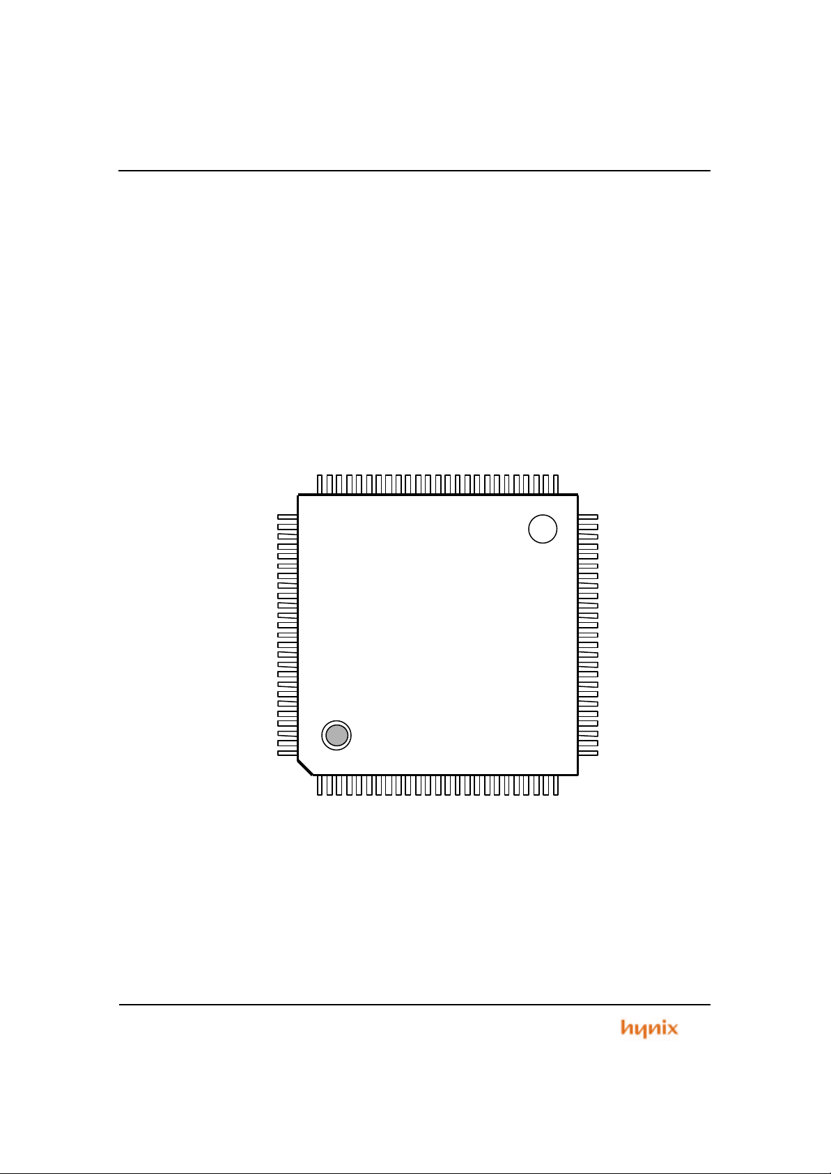
Figure 1.1 Package Outline ........................................................................................14
Figure 1.2 HMS39C7092 Block Diagram .................................................................... 15
Figure 1.3 HMS39C7092 Memory Map....................................................................... 25
Figure 1.4 Memory Map of Mode 3 .............................................................................25
Figure 1.5 Memory Map of when Mode 4 and Mode 5 ................................................. 26
Figure 1.6 Memory Map of Mode 6 and Mode 7 .......................................................... 26
Figure 2.1 ARM7TDMI Core Block Diagram ................................................................29
Figure 2.2 ARM instruction set formats .......................................................................30
Figure 2.3 Register Organization in ARM state............................................................ 32
Figure 2.4 THUMB instruction set formats................................................................... 33
Figure 2.5 Register Organization in THUMB state .......................................................35
Figure 2.6 Mapping of THUMB state registers onto ARM state registers. ...................... 35
Figure 2.7 Program status register format ................................................................... 36
Figure 3.1 Block Diagram of the Bus Controller ........................................................... 48
Figure 3.2 Access Area Map for Each Operating Mode................................................ 52
Figure 3.3 Access Size and Data Alignment Control (8 -Bit Access Area) ......................54
Figure 3.4 Access Size and Data Alignment Control (16-Bit Access Area) .................... 55
Figure 3.5 Bus Control Signal Write Timing for 16 -Bit, 1-Wait (Word Access)................ 56
Figure 3.6 Bus Control Signal Read Timing for 16 -Bit, 1-Wait (Word Access)................56
Figure 3.7 Bus Control Signal Write Timing for 16 -Bit, 1-Wait (Half-word Access) ..........57
Figure 3.8 Bus Control Signal Read Timing for 16 -Bit, 1-Wait (Half-word Access)..........57
Figure 3.9 Bus Control Signal Write Timing for 16 -Bit, 1-Wait (Byte Access).................. 58
Figure 3.10 Bus Cont rol Signal Read Timing for 16-Bit, 1-Wait (Byte Access)................58
Figure 3.11 Bus Control Signal Write Timing for 16-Bit, 2-Wait (Word Access)............... 59
Figure 3.12 Bus Control Signal Read Timing for 16-Bit, 2-Wait (Word Access).............. 59
Figure 3.13 Bus Control Signal Write Timing for 16-Bit, 2-Wait (Half-Word Access)........ 60
Figure 3.14 Bus Control Signal Read Timing for 16-Bit, 2-Wait (Half-Word Access)....... 60
Figure 3.15 Bus Control Signal Write Timing for 16-Bit, 2-Wait (Byte Access)................ 61
Figure 3.16 Bus Control Signal Read Timing for 16-Bit, 2-Wait (Byte Access)................ 61
Figure 3.17 Example of Wait State Insertion Timing. .................................................... 62
Figure 3.18 Example of External Bus Master Operation ...............................................64
Figure 5.1 PMU Block Diagram .................................................................................. 74
Figure 5.2 Reset and Powe r Management State Machine............................................76
Figure 5.3 Power on Reset Timing Diagram ................................................................81
Figure 5.4 Watch Dog Timer Overflow Timing Diagram ................................................81
Figure 5.5 Soft Reset (from WDT) Timing Diagram ......................................................82
Figure 5.6 Soft Reset (from PMU) Timing Diagram ......................................................82
Figure 6.1 Interrupt Control Flow Diagram .................................................................. 84
Figure 7.1 Watchdog Timer Module Block Diagram ..................................................... 92
Figure 7.2 Operation in the Watchdog Timer Mode ......................................................94
Figure 7.3 Operation in the Interval Timer Mode ..........................................................95
Figure 7.4 Interrupt Clear in the Interval Timer Mode ................................................. 100
Figure 7.5 Interrupt Clear in the Watchdog Timer Mode with Reset Disable.................101
Figure 7.6 Interrupt Clear in the Watchdog Timer Mode with Power-on Reset ..............102
Figure 7.7 Interrupt Clear in the Watchdog Timer Mode with Manual Reset .................103
Figure 8.1 General-purpose Timer Unit Module Block Diagram ..................................106
Preliminary 7
Page 8

Flash MCU(HMS39C7092)
Figure 8.2 Free-Running Counter Operation ............................................................. 115
Figure 8.3 Periodic Counter Operation ......................................................................116
Figure 8.4 Example of 0 Output/1 Output .................................................................. 117
Figure 8.5 Example of Toggle Output ........................................................................ 118
Figure 8.6 Compare Match Signal Output Timing ...................................................... 118
Figure 8.7 Input Capture Operation .......................................................................... 119
Figure 8.8 Synchronized Operation Example ............................................................120
Figure 8.9 PWM Mode Operation Example 1 ............................................................121
Figure 8.10 PWM Mode Operation Example 2...........................................................122
Figure 8.11 Reset-Synchronized PWM Mode Operation Example ...............................123
Figure 9.1 TOP BLOCK Diagram .............................................................................126
Figure 9.2 Internal UART Diagram ...........................................................................128
Figure 10.1 GPIO Block Diagram and PADS Connections(example for Port A and Port B)
.........................................................................................................................144
Figure 12.1 Block Diagram of Flash Memory ............................................................. 154
Figure 12.2 System Configuration When Using On -Board Boot Mode......................... 161
Figure 12.3 Boot Mode Execution Procedure ............................................................162
Figure 12.4 User Mode Execution Procedure ............................................................164
Figure 12.5 Flash Program & Program Verify Sequence ............................................167
Figure 12.6 Flash Pre-program & Pre -program Verify Sequence ................................169
Figure 12.7 Flash Erase & Erase Verify Sequence ....................................................171
Figure 12.8 Flash Erase Algorithm ...........................................................................172
Figure 12.9 Timing Diagram of Read ........................................................................175
Figure 12.10 Timing Diagram of Pre -Program/Program.............................................176
Figure 12.11 Timing Diagram of Erase ......................................................................176
Figure 12.12 Timing Diagram of Pre -Program/Program Verify ....................................177
Figure 12.13 Timing Diagram of Erase Verify ............................................................177
Figure 13.1 Block Diagram of A/D Converter.............................................................180
Figure 13.2 A/D converter Operation ........................................................................185
Figure 13.3 Example of Analog Input Circuit .............................................................188
Figure 13.4 A/D Converter Accuracy Definitions (1) ...................................................188
Figure 13.5 A/D Converter Accuracy Definitions (2) ...................................................189
Figure 14.1 The settling time of the crystal oscillator ..................................................197
Figure 14.2 Reset Input Timing ................................................................................197
Figure 14.3 The Write Timing Diagram of the Bus Controller ......................................198
Figure 14.4 The Read Timing Diagram of the Bus Controller ...................................... 198
Figure 14.5 Basic Bus Cycle with External Wait State................................................199
Figure 14.6 Bus Release Mode Timing .....................................................................199
8 Preliminary
Page 9

Flash MCU(HMS39C7092)
Tables
Table 1.1 Pin Descriptions ......................................................................................... 16
Table 1.1 Pin Descriptions (Continued) ....................................................................... 17
Table 1.1 Pin Descriptions (Continued) ....................................................................... 18
Table 1.1 Pin Descriptions (Continued) ....................................................................... 19
Table 1.1 Pin Descriptions (Continued) ....................................................................... 20
Table 1.2 HMS39C7092 Operation modes .................................................................. 21
Table 1.3 Pin assignment by mode .............................................................................22
Table 1.3 Pin assignment by mode (continued) ........................................................... 23
Table 1.3 Pin assignment by mode (continued) ........................................................... 24
Table 2.1 The ARM Instruction set ..............................................................................31
Table 2.2 THUMB instruction set opcodes ...................................................................34
Table 2.3 Condition code summary .............................................................................36
Table 2.4 PSR mode bit values .................................................................................. 38
Table 3.1 Bus Controller Pins ..................................................................................... 49
Table 3.2 BUS Controller Register Map .......................................................................50
Table 3.3 Byte Lane condition by XA[0] .......................................................................55
Table 4.1 Pin Function Descriptions............................................................................ 66
Table 4.2 Memory map of the MCU Controller .............................................................67
Table 4.3 MCU Controller Initial values in each mode .................................................. 67
Table 5.1 Register Map of the PMU ............................................................................ 77
Table 6.1 Interrupt Controller Default Setting Value...................................................... 85
Table 6.2 Memory Map of the Interrupt Controller ........................................................ 87
Table 6.3 Interrupt Source Trigger Mode .....................................................................88
Table 7.1 Memory Map of the Watchdog Timer APB Peripheral.................................... 96
Table 7.2 Internal Counter Clock Sources (SYSCLK = 40 MHz).................................... 98
Table 8.1 Timer Global Control Register Map ............................................................108
Table 8.2 Timer Channel Control Register Map .........................................................108
Table 8.3 Timer Channel Starting Address ................................................................108
Table 9.1 Signal Descriptions ...................................................................................127
Table 9.2 UART Register Address Map (0x1500 in UART1) .......................................129
Table 9.3 UART Register Reset Values .....................................................................129
Table 9.4a Divisor Values for each Baud rate (CLK=1.8432MHz)................................133
Tab le 9.4b Divisor Values for each Baud rate (CLK=3.6864MHz)................................ 133
Table 9.5 Interrupt Control Functions ........................................................................138
Table 9.6 Summary of Registers ............................................................................... 142
Table 10.1 GPIO Register Memory Map ....................................................................145
Table 12.1 Operating mode......................................................................................153
Table 12.2 Signal description of Figure 12.1(BUS Interface) ....................................... 155
Table 12.3 Flash Memory Registers ..........................................................................156
Table 12.4 Control Register ...................................................................................... 158
Table 12.5 Erase Block Register ...............................................................................159
Table 12.6 Status & Power Register .........................................................................160
Table 12.7 FR_SEL Value for access to internal Register...........................................173
Table 12.8 Setting for Register read/write..................................................................173
Table 12.9 Erase Block Register ...............................................................................174
Table 12.10 Setting for Flash PROM read/write ......................................................... 175
Preliminary 9
Page 10

Flash MCU(HMS39C7092)
Table 12.11 DC Characteristics ................................................................................178
Table 12.12 AC Characteristics ................................................................................178
Table 13.1 A/D Converter Pins .................................................................................181
Table 13.2 Summarizes the A/D convert er’s registers................................................182
Table 14.1 Absolute Maximum Ratings - Preliminary -............192
Table 14.2 Recommended Operating Conditions - Preliminary - .............192
Table 14.3 DC Characteristics - Preliminary - ..........193
Table 14.4 IO Circuits with pull-ups - Preliminary - ...........193
Table 14.5 IO Circuits with pull-downs - Preliminary - ............193
Table 14.6 Clock Timing - Preliminary -...........194
Table 14.7 Control Signal Timing - Preliminary - ...........194
Table 14.8 Bus Timing - Preliminary -..........195
Table 14.9 Operating Conditions of the AD Conversion - Preliminary -.............196
Table 14.10 Electrical characteristics of the AD converter - Preliminary -.............196
10 Preliminary
Page 11

Flash MCU(HMS39C7092)
Preliminary 11
Page 12

Flash MCU(HMS39C7092)
12 Preliminary
Page 13

Flash MCU(HMS39C7092) Introduction
Chapter 1
Introduction
Preliminary 13
Page 14
Introduction Flash MCU(HMS39C7092)
1.1 General Description
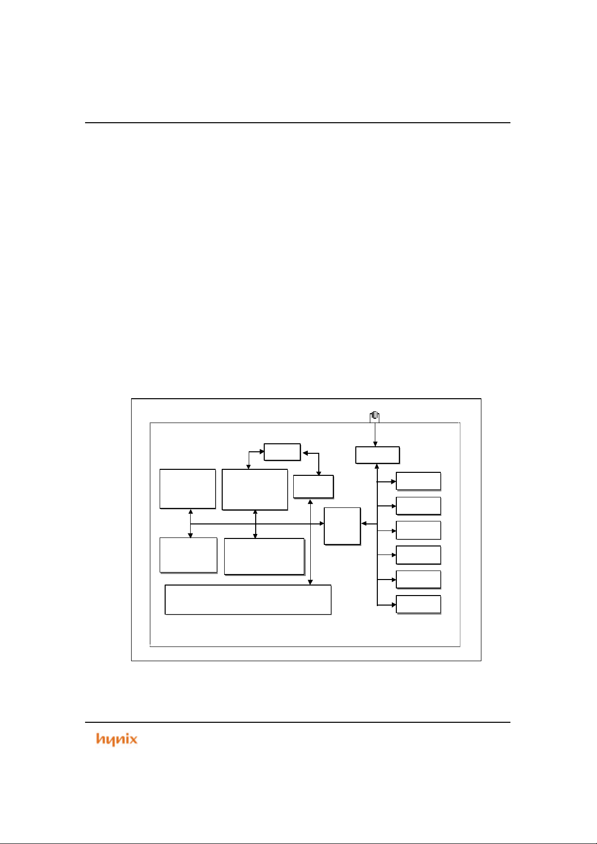
The 16bit MCU with embedded flash memory for optical storage is the first member
of Hynix Micro Electronics 16/32bit MCU Family of high performance microcontroller
units (MCUs). This family includes a series of peripherals from which numerous
MCUs are assembled. Th is MCU contains extensive peripherals : 192Kbytes flas h
memory, 4K bytes SRAM, 6 channel 16bit Timer, Watch Dog Timer, 2 channel UART,
Programmable Priority Interrupt Controller, 81bits PIO, BUS Controller including Chip
select logic, which is On-Chip Modular Architecture (using AMBA).
nBREQ/P6
nBACK/P6
MODE
1
2
MODE
MODE
0
VDD
XTALOUT
XTALIN
VSS
nTRST/P9
nRES
7
nHWR/P6
nLWR/P6
nRD/P6
nAS/P6
3
4
5
6
CLKO/P6
nSTBY
7
nWAIT/P6
A
A
A
A
A
A
19
/P53VSS
0
1
2
14
15
16
17
18
/P2
/P2
/P5
/P5
/P5
6
7
0
1
2
AVDD
AV
AN0/P7
AN0/P7
AN0/P7
AN0/P7
AN0/P7
TIOCA5/nIRQ6/P7
TIOCB5/nIRQ7/P7
nCS3/nIRQ1/P8
nCS2/nIRQ2/P8
nCS1/nIRQ3/P8
TCLKC/TCIOA0/PA
TCLKD/TCIOB0/PA
VSS
nIRQ0/P8
nCS0/P8
VSS
TCLKA/PA
TCLKB/PA
A23/TIOCA1/PA
A22/TIOCB1/PA
A21/TIOCA2/PA
A20/TIOCB2/PA
75
74
73
72
71
70
69
68
76
REF
P7
77
78
0
79
1
80
2
81
3
82
4
83
84
6
85
7
86
5
87
0
88
1
89
2
90
3
91
4
92
93
0
94
1
95
2
96
3
97
4
98
5
99
6
100
7
HMS39C7092
2001.02
1
2
3
4
5
6
7
8
0
1
2
3
5
/PB
/PB
4
4
/TIOCA
/TIOCB
5
4
6
TDI/PB
TMS/PB4TDO/PB
VDD
/PB
/PB
3
3
/TIOCA
/TIOCB
7
6
67
66
9
7
TCK/PB
10
XP9
63
65
64
62
61
60
59
58
57
56
55
54
53
52
51
A13/P2
50
49
48
47
46
45
44
43
42
41
40
39
38
37
36
35
34
33
32
31
30
29
28
27
11
12
13
14
15
16
17
18
19
20
21
0
2
4
1
/P9
0
RxD
/P9
1
TxD
3
/P9
1
RxD
/P9
4
nIRQ
5
/P9
5
nIRQ
/P4
D
0
0
2
3
/P4
/P4
/P4
0
0
2
3
D
D
D
6
/P9
VSS
0
TxD
22
VSS
23
/P4
D
26
24
25
4
5
6
/P4
/P4
4
5
6
D
D
A12/P2
A11/P2
A10/P2
A9/P2
A8/P2
VSS
A7/P1
A6/P1
A5/P1
A4/P1
A3/P1
A2/P1
A1/P1
A0/P1
VDD
D15/P3
D14/P3
D13/P3
D12/P3
D11/P3
D10/P3
D9/P3
/P3
D8
D7/P4
5
4
3
2
1
0
7
6
5
4
3
2
1
0
7
6
5
4
3
2
1
0
7
Figure 1.1 Package Outline
14 Preliminary
Page 15
Flash MCU(HMS39C7092) Introduction
1.2 Feature
• On-Chip Modular Architecture (using AMBA)
• Utilizes the ARM7TDMI 32/16bit RISC Family
• 192Kbyte flash memory
• 4Kbyte internal SRAM
• 8/16-bit external Data Bus
• Eight Programmable Chip Select Output s with external wait input
• Low Power Consumption using Power Management Unit
• Fully static operation : Max. 50MHz
• Programmable Priority Interrupt Controller (8 external sources)
• Six 16bit Multi Function Timers/Counters for General Purpose Applications
• One 8bit Watch Dog Timer (WDT)
• Two UARTs (Universal Asynchronous Receiver Transmitter) compatible with
16C550 UART
• Programmable Input/Output ports (81-bits)
• 100 TQFP Package
BUS
BUS
Controller
Controller
SRAM
SRAM
4kbyte
4kbyte
Arbiter
Arbiter
ARM7TDMI
ARM7TDMI
ASB (Max. 50MHz)
Flash Memory
Flash Memory
192kbyte
192kbyte
Multi-Function Pin MUX
Multi-Function Pin MUX
TIC*
TIC*
APB
APB
Bridge
Bridge
* TIC : Test Interface Controller
PMU
PMU
Figure 1.2 HMS39C7092 Block Diagram
Max. 50MHz
PIO
INTC
INTC
WDT
WDT
TIMER
TIMER
UART
UART
ADC
ADC
PIO
Preliminary 15
Page 16
Introduction Flash MCU(HMS39C7092)
1.3 Pin Descriptions
Table 1.1 Pin Descriptions
PIN SYMBOL DIR DESCRIPTION
1 VDD - Power Supply 3.3V
nCS7 O External Chip Selection Number 7
2
TCIOA3 I/O PWM output, Compare match output of Reg.A and signal capture input of Timer Ch3
PB0 I/O General purpose input output of port B bit0
nCS6 O External Chip Selection Number 6
3
TCIOB3 I/O PWM output, Compare match output of Reg.B and signal capture input of Timer Ch3
PB1 I/O General purpose input output of port B bit 1
nCS5 O External Chip Selection Number 5
4
TIOCA4 I/O PWM output, Compare match output of Reg.A and signal capture input of Timer Ch4
PB2 I/O General purpose input output of port B bit2
nCS4 O External Chip Selection Number 4
5
TIOCB4 I/O PWM output, Compare match output of Reg.B and signal capture input of Timer Ch4
PB3 I/O General purpose input output of port B bit3
6
7
8
9
10 TVPPD I 5Vinput for the use of Programming and Erasing of the Flash Memory
11 VSS - Power ground
12
13
14
15
16
17
18
19
20
21
TMS I JTAG Test Mode Selection
PB4 I/O General purpose input output of port B bit4
TDO O JTAG Test Data Output
PB5 I/O General purpose input output of port B bit5
TDI I JTAG Test Data Input
PB6 I/O General purpose input output of port B bit6
TCK I JTAG Test Clock
PB7 I/O General purpose input output of port B bit7
TxD0 O Transmit Data of UART Ch0
P90 I/O General purpose input output of port 9 bit 0
RxD0 O Receive Data of UART Ch0
P91 I/O General purpose input output of port 9 bit 1
TxD1 O Transmit Data of UART Ch1
P92 I/O General purpose input output of port 9 bit 2
RxD1 O Receive Data of UART Ch1
P93 I/O General purpose input output of port 9 bit 3
nIRQ4 I External Interrupt Request number 4
P94 I/O General purpose input output of port 9 bit 4
nIRQ5 I External Interrupt Request number 5
P95 I/O General purpose input output of port 9 bit 5
D0 I/O External Data Bus bit 0
P40 I/O General purpose input output or port 4 bit 0
D1 I/O External Data Bus bit 1
P41 I/O General purpose input output or port 4 bit 1
D2 I/O External Data Bus bit 2
P42 I/O General purpose input output or port 4 bit 2
D3 I/O External Data Bus bit 3
P43 I/O General purpose input output or port 4 bit 3
16 Preliminary
Page 17

Flash MCU(HMS39C7092) Introduction
Table 1.1 Pin Descriptions (Continued)
PIN SYMBOL DIR DESCRIPTION
22 VSS - Power ground
23
24
25
26
27
28
29
30
31
32
33
34
35 VDD - Power Supply 3.3V
36
37
38
39
40
41
42
43
44 VSS - Power ground
45
46
47
D4 I/O External Data Bus bit 4
P44 I/O General purpose input output or port 4 bit 4
D5 I/O External Data Bus bit 5
P45 I/O General purpose input output or port 4 bit 5
D6 I/O External Data Bus bit 6
P46 I/O General purpose input output or port 4 bit 6
D7 I/O External Data Bus bit 7
P47 I/O General purpose input output or port 4 bit 7
D8 I/O External Data Bus bit 8
P30 I/O General purpose input output or port 3 bit 0
D9 I/O External Data Bus bit 9
P31 I/O General purpose input output or port 3 bit 1
D10 I/O External Data Bus bit 10
P32 I/O General purpose input output or port 3 bit 2
D11 I/O External Data Bus bit 11
P33 I/O General purpose input output or port 3 bit 3
D12 I/O External Data Bus bit 12
P34 I/O General purpose input output or port 3 bit 4
D13 I/O External Data Bus bit 13
P35 I/O General purpose input output or port 3 bit 5
D14 I/O External Data Bus bit 14
P36 I/O General purpose input output or port 3 bit 6
D15 I/O External Data Bus bit 15
P37 I/O General purpose input out put or port 3 bit 7
A0 O External Address Bus bit 0
P10 I/O General purpose input output or port 1 bit 0
A1 O External Address Bus bit 1
P11 I/O General purpose input output or port 1 bit 1
A2 O External Address Bus bit 2
P12 I/O General purpose input output or port 1 bit 2
A3 O External Address Bus bit 3
P13 I/O General purpose input output or port 1 bit 3
A4 O External Address Bus bit 4
P14 I/O General purpose input output or port 1 bit 4
A5 O External Address Bus bit 5
P15 I/O General purpose input output or port 1 bit 5
A6 O External Address Bus bit 6
P16 I/O General purpose input output or port 1 bit 6
A7 O External Address Bus bit 7
P17 I/O General purpose input output or port 1 bit 7
A8 O External Address Bus bit 8
P20 I/O General purpose input output or port 2 bit 0
A9 O External Address Bus bit 9
P21 I/O General purpose input output or port 2 bit 1
A10 O External Address Bus bit 10
P22 I/O General purpose input output or port 2 bit 2
Preliminary 17
Page 18

Introduction Flash MCU(HMS39C7092)
Table 1.1 Pin Descriptions (Continued)
PIN SYMBOL DIR DESCRIPTION
48
49
50
51
52
53
54
55
56
57 VSS - Power ground
58
59
60
61
62 nSTBY O Standby mode signal. Power Down mode indicating
63 nRES I External Reset input
64
65 VSS - Power ground
66 XTALOUT O Crystal feedback output
67 XTALIN I Crystal or External Oscillator input
68 VDD - Power Supply 3.3V
69
70
71
72
73 MODE0 I MODE bit 0
74 MODE1 I MODE bit 1
75 MODE2 I MODE bit 2
76 AVDD - Analog Power Supply 3.3V
77 AVREF - ADC Reference Voltage
A11 O External Address Bus bit 11
P23 I/O General purpose input output or port 2 bit 3
A12 O External Address Bus bit 12
P24 I/O General purpose input output or port 2 bit 4
A13 O External Address Bus bit 13
P25 I/O General purpose input output or port 2 bit 5
A14 O External Address Bus bit 14
P26 I/O General purpose input output or port 2 bit 6
A15 O External Address Bus bit 15
P27 I/O General purpose input output or port 2 bit 7
A16 O External Address Bus bit 16
P50 I/O General purpose input output of port 5 bit 0
A17 O External Address Bus bit 17
P51 I/O General purpose input output of port 5 bit 1
A18 I External Address Bus bit 18
P52 I/O General purpose input output of port 5 bit 2
A19 O External Address Bus bit 19
P53 I/O General purpose input output of port 5 bit 3
nWAIT I External BUS cycle wait signal
P60 I/O General purpose input output of port 6 bit 0
nBREQ I External BUS Request
P61 I/O General purpose input output of port 6 bit 1
nBACK I External BUS Acknowledge
P62 I/O General purpose input output of port 6 bit 2
CLKO O BUS Clock Output
P67 I/O General purpose input output of port 6 bit 7
nTRST I JTAG Test Reset input
P97 I/O General purpose input output of port 9 bit 7
nAS O External Address Bus strobe
P63 I/O General purpose input output of port 6 bit 3
nRD O External Bus Read
P64 I/O General purpose input output of port 6 bit 4
nHWR O External upper 8 bit data bus write
P65 I/O General purpose input output of port 6 bit 5
nLWR O External lower 8 bit data bus write
P66 I/O General purpose input output of port 6 bit 6
18 Preliminary
Page 19

Flash MCU(HMS39C7092) Introduction
Table 1.1 Pin Descriptions (Continued)
PIN SYMBOL DIR DESCRIPTION
78
79
80
81
82
83 VSS - Power ground
85
86 P75 I/O General purpose input output of port 7 bit 5
87
89
91
92 VSS - Power ground
93
94
95
96
97
P70 O General purpose output of port 7 bit 0
AN0 I ADC Channel 0 input
P71 O General purpose output of port 7 bit 1
AN1 I ADC Channel 1 input
P72 O General purpose output of port 7 bit 2
AN2 I ADC Channel 2 input
P73 O General purpose output of port 7 bit 3
AN3 I ADC Channel 3 input
P74 O General purpose output of port 7 bit 4
AN4 I ADC Channel 4 input
TIOCA5 I/O PWM output, Compare match output of Reg.A and signal capture input of Timer Ch5
nIRQ6 I External Interrupt Request number 6 84
P76 I/O General purpose input output of port 7 bit 6
TIOCB5 I/O PWM output, Compare match output of Reg.B and signal capture input of Timer Ch5
nIRQ7 I External Interrupt Request number 7
P77 I/O General purpose input output of port 7 bit 7
nIRQ0 I External Interrupt Request number 0
P80 I/O General purpose input output of port 8 bit 0
nCS3 O External Chip Selection Number 3
nIRQ1 I External Interrupt Request number 1 88
P81 I/O General purpose input output of port 8 bit 1
nCS2 O External Chip Selection Number 2
nIRQ2 I External Interrupt Request number 2
P82 I/O General purpose input output of port 8 bit 2
nCS1 O External Chip Selection Number 1
nIRQ3 I External Interrupt Request number 3 90
P83 I/O General purpose input output of port 8 bit 3
nCS0 O External Chip Selection Number 0
P84 I/O General purpose input output of port 8 bit 4
TCLKA I External timer input clock A
PA0 I/O General purpose input output of port A bit 0
TCLKB I External timer input clock B
PA1 I/O General purpose input output of port A bit 1
TCLKC I External timer input clock C
TIOCA0 I/O PWM output, Compare match output of Reg.A and signal capture input of Timer Ch0
PA2 I/O General purpose input output of port A bit 2
TCLKD I External timer input clock D
TIOCB0 I/O PWM output, Compare match output of Reg.B and signal capture input of Timer Ch0
PA3 I/O General purpose input output of port A bit 3
A23 O External Address Bus bit 23
TIOCA1 I/O PWM output, Compare mat ch output of Reg.A and signal capture input of Timer Ch1
PA4 I/O General purpose input output of port A bit 4
Preliminary 19
Page 20

Introduction Flash MCU(HMS39C7092)
Table 1.1 Pin Descriptions (Continued)
PIN SYMBOL DIR DESCRIPTION
98
99
100
A22 O External Address Bus bit 22
TIOCB1 I/O PWM output, Compare match output of Reg.B and signal capture input of Timer Ch1
PA5 I/O General purpose input output of port A bit 5
A21 O External Address Bus bit 21
TIOCA2 I/O PWM output, Compare match output of Reg.A and signal capture input of Timer Ch2
PA6 I/O General purpose input output of port A bit 6
A20 O External Address Bus bit 20
TIOCB2 I/O PWM output, Compare match output of Reg.B and signal capture input of Timer Ch2
PA7 I/O General purpose input output of port A bit 7
20 Preliminary
Page 21

Flash MCU(HMS39C7092) Introduction
1.4 Operation Mode description
HMS39C7092 is Flash Memory-embedded ARM microcontroller. It has six-operation
modes shown in Table 1.2. HMS39C7092 External pin function is changed by setting
external MODE pin or configuring the PIN MUX registers. The pin assignment by
mode is shown in Table 1.3 . Especially changing mode causes memory remap for
appropriate mode. Figure 1.3 shows default memory map and the memory maps of
respective modes are shown in Figure 1.4, Figure 1.5 and Figure 1.6.
The Mode definition is listed as follows:
Table 1.2 HMS39C7092 Operation modes
MODE MODE DESCRIPTION
0,1 Reserved for Test
2 External 8-bit data bus with 16MBytes of Address Range
3 External 16-bit data bus with 16MBytes of Address Range
4 Flash-boot mode with 16-bit data bus
5 Flash-boot mode (micro-computer mode)
6 UART-boot mode with 16-bit data bus
7 UART-boot mode (micro-computer mode)
Preliminary 21
Page 22

Introduction Flash MCU(HMS39C7092)
Table 1.3 Pin assignment by mode
MODE 2 MODE 3 MODE 4 MODE 6 MODE 5 MODE 7 PIN
External
8bit BUS
1
2
3
4
5
6
7
8
9
10
11
12
13
14
15
16
17
18
19
20
21
22
23
24
25
26
27
28
29
30
31
32
33
34
35
36
37
38
39
40
VDD
nCS7
nCS6
nCS5
nCS4
TMS
TDO
TDI
TCK
TVPPD
VSS
TxD0
RxD0
TxD1
RxD1
nIRQ4
nIRQ5
D0
D1
D2
D3
VSS
D4
D5
D6
D7
P30 D8
P31 D9
P32 D10
P33 D11
P34 D12
P35 D13
P36 D14
P37 D15
VDD
A0
A1
A2
A3
A4
External
16bit BUS
ß ß ß ß ß
ß ß ß
ß ß ß
ß ß ß
ß ß ß
ß ß ß ß ß
ß ß ß ß ß
ß ß ß ß ß
ß ß ß ß ß
ß ß ß ß ß
ß ß ß ß ß
ß ß ß ß ß
ß ß ß ß ß
ß ß ß ß ß
ß ß ß ß ß
ß ß ß ß ß
ß ß ß ß ß
ß ß ß
ß ß ß
ß ß ß
ß ß ß
ß ß ß ß ß
ß ß ß
ß ß ß
ß ß ß
ß ß ß
ß ß ß ß ß
ß ß ß
ß ß ß
ß ß ß
ß ß ß
ß ß ß
Flash boot mode
with 16bit BUS
ß ß
ß ß
ß ß
ß ß
ß ß
ß ß
ß ß
ß ß
UART boot mode
with 16bit BUS
Flash boot mode
(MICOM mode)
TIOCA3
TIOCB3
TIOCA4
TIOCB4
P40
P41
P42
P43
P44
P45
P46
P47
P30
P31
P32
P33
P34
P35
P36
P37
P10
P11
P12
P13
P14
UART boot mode
(MICOM mode)
ß
ß
ß
ß
ß
ß
ß
ß
ß
ß
ß
ß
ß
ß
ß
ß
ß
ß
ß
ß
ß
ß
ß
ß
ß
22 Preliminary
Page 23

Flash MCU(HMS39C7092) Introduction
Table 1.3 Pin assignment by mode (continued)
MODE2 MODE3 MODE4 MODE6 MODE5 MODE7 PIN
No.
41
42
43
44
45
46
47
48
49
50
51
52
53
54
55
56
57
58
59
60
61
62
63
64
65
66
67
68
69
70
71
72
73
73
75
76
77
78
79
80
External
8bit BUS
A5
A6
A7
VSS
A8
A9
A10
A11
A12
A13
A14
A15
A16
A17
A18
A19
VSS
nWAIT
nBREQ
nBACK
CLKO
nSTBY
nRES
nTRST
VSS
XTALOUT
XTALIN
VDD
nAS
nRD
nHWR
nLWR
MODE0
MODE1
MODE2
AVDD
AVREF
AN0
AN1
AN2
External
16bit BUS
ß ß ß
ß ß ß
ß ß ß
ß ß ß ß ß
ß ß ß
ß ß ß
ß ß ß
ß ß ß
ß ß ß
ß ß ß
ß ß ß
ß ß ß
ß ß ß
ß ß ß
ß ß ß
ß ß ß
ß ß ß ß ß
ß ß ß
ß ß ß
ß ß ß
ß ß ß
ß ß ß
ß ß ß
ß ß ß
ß ß ß ß ß
ß ß ß ß ß
ß ß ß ß ß
ß ß ß ß ß
ß ß ß
ß ß ß
ß ß ß
ß ß ß
ß ß ß ß ß
ß ß ß ß ß
ß ß ß ß ß
ß ß ß ß ß
ß ß ß ß ß
ß ß ß ß ß
ß ß ß ß ß
ß ß ß ß ß
Flash boot mode
with 16bit BUS
UART boot mode
with 16bit BUS
Flash boot mode
(MICOM mode)
P15
P16
P17
P20
P21
P22
P23
P24
P25
P26
P27
P50
P51
P52
P53
P60
P61
P62
P67
nSTBY
nRES
nTRST
P63
P64
P65
P66
UART boot mode
(MICOM mode)
ß
ß
ß
ß
ß
ß
ß
ß
ß
ß
ß
ß
ß
ß
ß
ß
ß
ß
ß
ß
ß
ß
ß
ß
ß
ß
Preliminary 23
Page 24

Introduction Flash MCU(HMS39C7092)
Table 1.3 Pin assignment by mode (continued)
MODE2 MODE3 MODE4 MODE6 MODE5 MODE7 PIN
No.
81
82
83
84
85
86
87
88
89
90
91
92
93
94
95
96
97
98
99
100
External
8bit BUS
AN3
AN4
VSS
TIOCA5
TIOCB5
P75
nIRQ0
nCS3
nCS2
nCS1
nCS0
VSS
TCLKA
TCLKB
TCLKC
TCLKD
A23
A22
A21
A20
External
16bit BUS
ß ß ß ß ß
ß ß ß ß ß
ß ß ß ß ß
ß ß ß ß ß
ß ß ß ß ß
ß ß ß ß ß
ß ß ß ß ß
ß ß ß
ß ß ß
ß ß ß
ß ß ß
ß ß ß ß ß
ß ß ß ß ß
ß ß ß ß ß
ß ß ß ß ß
ß ß ß ß ß
ß ß
ß ß
ß ß
ß ß
Flash boot mode
with 16bit BUS
UART boot mode
with 16bit BUS
TIOCA1
TIOCB1
TIOCA2
TIOCB2
Flash boot mode
(MICOM mode)
P81
P82
P83
P84
ß ß
ß ß
ß ß
ß ß
UART boot mode
(MICOM mode)
ß
ß
ß
ß
24 Preliminary
Page 25
Flash MCU(HMS39C7092) Introduction
1.5 Memory Map
0xFFFF FFFF
0x0900 2000
0x0900 1FFF
0x0900 1000
0x0900 0FFF
0x0900 0000
0x0804 FFFF
0x0804 0000
0x0803 FFFF
0x0803 0000
0x0802 FFFF
0x0800 0000
0x07FF FFFF
0x0000 0000
nCS7
nCS6
nCS5
nCS4
nCS3
nCS2
nCS1
0x07FF FFFF
0x0700 0000
0x06FF FFFF
0x0600 0000
0x05FF FFFF
0x0500 0000
0x04FF FFFF
0x0400 0000
0x03FF FFFF
0x0300 0000
0x02FF FFFF
0x0200 0000
0x01FF FFFF
0x0100 0000
0x00FF FFFF
nCS0
0x0000 0000
Default.
SM=0 in the PMU register.
Reserved
Reserved
APB Register
ASB Register
Reserved
On Chip
BOOT ROM
On Chip
SRAM(4KB)
FLASH
nCS0 ~ nCS7
Chip Select
Area
Reserved
ARM7TEST
Figure 1.3 HMS39C7092 Memory Map
0x07FF FFFF
nCS7
Reserved
0x0080 0000
nCS7
nCS6
nCS5
nCS4
nCS3
nCS2
nCS1
nCS0
SM=1 in the PMU register. Remap mode (Remap =1)
0x007F FFFF
0x0070 0000
0x006F FFFF
0x0060 0000
0x005F FFFF
0x0050 0000
0x004F FFFF
0x0040 0000
0x003F FFFF
0x0030 0000
0x002F FFFF
0x0020 0000
0x001F FFFF
0x0010 0000
0x000F FFFF
0x0000 0000
nCS6
nCS5
nCS4
nCS3
nCS2
nCS1
nCS0
On Chip
SRAM
SM=0 in the PMU register.
0x07FF FFFF
0x0700 0000
0x06FF FFFF
0x0600 0000
0x05FF FFFF
0x0500 0000
0x04FF FFFF
0x0400 0000
0x03FF FFFF
0x0300 0000
0x02FF FFFF
0x0200 0000
0x01FF FFFF
0x0100 0000
0x00FF FFFF
0x0000 1000
0x0000 0FFF
0x0000 0000
ADC
GPIO
UART1
UART0
TIMER
INTC
WDT
PMU
FMI
SMI
MCUC
Reserved
nCS7
nCS6
nCS5
nCS4
nCS3
nCS2
nCS1
nCS0
On Chip
SRAM
Remap mode (Remap =1)
SM=1 in the PMU register.
0x0900 1FFF
0x0900 1800
0x0900 17FF
0x0900 1700
0x0900 16FF
0x0900 1600
0x0900 15FF
0x0900 1500
0x0900 14FF
0x0900 1400
0x0900 13FF
0x0900 1300
0x0900 12FF
0x0900 1200
0x0900 11FF
0x0900 1100
0x0900 10FF
0x0900 1000
0x0900 0FFF
0x0900 0400
0x0900 03FF
0x0900 0300
0x0900 02FF
0x0900 0200
0x0900 01FF
0x0900 0100
0x0900 00FF
0x0900 0000
0x07FF FFFF
0x0080 0000
0x007F FFFF
0x0070 0000
0x006F FFFF
0x0060 0000
0x005F FFFF
0x0050 0000
0x004F FFFF
0x0040 0000
0x003F FFFF
0x0030 0000
0x002F FFFF
0x0020 0000
0x001F FFFF
0x0010 0000
0x000F FFFF
0x0000 1000
0x0000 0FFF
0x0000 0000
Figure 1.4 Memory Map of Mode 3
Preliminary 25
Page 26
Introduction Flash MCU(HMS39C7092)
nCS7
nCS6
nCS5
nCS4
nCS3
nCS2
nCS1
nCS0
FLASH
(192KB)
Default.
SM=0 in the PMU register.
0 x07FF FFFF
0x0700 0000
0 x06FF FFFF
0x0600 0000
0 x05FF FFFF
0x0500 0000
0 x04FF FFFF
0x0400 0000
0 x03FF FFFF
0x0300 0000
0 x02FF FFFF
0x0200 0000
0 x01FF FFFF
0x0100 0000
0 x00FF FFFF
0x0003 0000
0 x0002 FFFF
0x0000 0000
Reserved
nCS7
nCS6
nCS5
nCS4
nCS3
nCS2
nCS1
nCS0
FLASH
(192KB)
SM=1 in the PMU register. Remap mode ( Remap=1)
0x07FF FFFF
0x0080 0000
0x007F FFFF
0x0070 0000
0x006F FFFF
0x0060 0000
0x005F FFFF
0x0050 0000
0x004F FFFF
0x0040 0000
0x003F FFFF
0x0030 0000
0x002F FFFF
0x0020 0000
0x001F FFFF
0x0010 0000
0x000F FFFF
0x0003 0000
0x0002 FFFF
0x0000 0000
nCS7
nCS6
nCS5
nCS4
nCS3
nCS2
nCS1
nCS0
FLASH
(192KB)
On Chip
SRAM(4KB)
SM=0 in the PMU register.
0x07FF FFFF
0x0700 0000
0x06FF FFFF
0x0600 0000
0x05FF FFFF
0x0500 0000
0x04FF FFFF
0x0400 0000
0x03FF FFFF
0x0300 0000
0x02FF FFFF
0x0200 0000
0x01FF FFFF
0x0100 0000
0x00FF FFFF
0x0003 0000
0x0002 FFFF
0x0000 1000
0x0000 0FFF
0x0000 0000
Reserved
nCS7
nCS6
nCS5
nCS4
nCS3
nCS2
nCS1
nCS0
FLASH
(192KB)
On Chip
SRAM(4KB)
Remap mode (Remap=1)
SM=1 in the PMU register.
Figure 1.5 Memory Map of when Mode 4 and Mode 5
nCS7
nCS6
nCS5
nCS4
nCS3
nCS2
nCS1
0x07FF FFFF
0x0700 0000
0x06FF FFFF
0x0600 0000
0x05FF FFFF
0x0500 0000
0x04FF FFFF
0x0400 0000
0x03FF FFFF
0x0300 0000
0x02FF FFFF
0x0200 0000
0x01FF FFFF
0x0100 0000
0x00FF FFFF
nCS0
0x0000 0100
On Chip
Boot ROM
(256Byte)
Default.
SM=0 in the PMU register.
0x0000 00FF
0x0000 0000
Reserved
nCS7
nCS6
nCS5
nCS4
nCS3
nCS2
nCS1
nCS0
On Chip
Boot ROM
(256Byte)
SM=1 and OnFLASH=0
in the PMU register.
0x07FF FFFF
0x0080 0000
0x007F FFFF
0x0070 0000
0x006F FFFF
0x0060 0000
0x005F FFFF
0x0050 0000
0x004F FFFF
0x0040 0000
0x003F FFFF
0x0030 0000
0x002F FFFF
0x0020 0000
0x001F FFFF
0x0010 0000
0x000F FFFF
0x0000 0100
0x0000 00FF
0x0000 0000
nCS7
nCS6
nCS5
nCS4
nCS3
nCS2
nCS1
nCS0
FLASH
(192KB)
SM=0 and On FLASH=1
in the PMU register.
0x07FF FFFF
0x0700 0000
0x06FF FFFF
0x0600 0000
0x05FF FFFF
0x0500 0000
0x04FF FFFF
0x0400 0000
0x03FF FFFF
0x0300 0000
0x02FF FFFF
0x0200 0000
0x01FF FFFF
0x0100 0000
0x00FF FFFF
0x0003 0000
0x0002 FFFF
0x0000 1000
0x0000 0FFF
0x0000 0000
0x07FF FFFF
Reserved
0x0080 0000
nCS7
nCS6
nCS5
nCS4
nCS3
nCS2
nCS1
nCS0
FLASH
(192KB)
SM=1 andOnFLASH =1
in the PMU register.
0x007F FFFF
0x0070 0000
0x006F FFFF
0x0060 0000
0x005F FFFF
0x0050 0000
0x004F FFFF
0x0040 0000
0x003F FFFF
0x0030 0000
0x002F FFFF
0x0020 0000
0x001F FFFF
0x0010 0000
0x000F FFFF
0x0003 0000
0x0002 FFFF
0x0000 1000
0x0000 0FFF
0x0000 0000
0x07FF FFFF
0x0080 0000
0x007F FFFF
0x0070 0000
0x006F FFFF
0x0060 0000
0x005F FFFF
0x0050 0000
0x004F FFFF
0x0040 0000
0x003F FFFF
0x0030 0000
0x002F FFFF
0x0020 0000
0x001F FFFF
0x0010 0000
0x000F FFFF
0x0003 0000
0x0002 FFFF
0x0000 1000
0x0000 0FFF
0x0000 0000
Figure 1.6 Memory Map of Mode 6 and Mode 7
26 Preliminary
Page 27

Flash MCU(HMS39C7092) ARM7TDMI Core
Chapter 2
ARM7TDMI Core
Preliminary 27
Page 28

ARM7TDMI Core Flash MCU(HMS39C7092)
2.1 General Description
The ARM7TDMI is a member of the ARM family of general-purpose 32bit
microprocessors, which offer s high performance for very low power consumption and
price. This processor employs a unique architectural strategy known as THUMB,
which makes it ideally suited to high volume applications with memory restrictions or
applications where code density is an issue.
The key idea behind THUMB is a super reduced instruction set. Essentially, the
ARM7TDMI has two instruction sets, the standard 32bit ARM set and 16bit THUMB
set. The THUMB set’s 16bit instruction length allows it to approach twice the density
of standard ARM code while retaining most of the ARM’s performance advantage
over a traditional 16bit processor by using 16bit registers. Th is is possible because
THUMB code operates on the same 32bit register set as ARM code.
See also ARM7TDMI Datasheet (ARM DDI 0029E) for detail.
2.2 Feature
• 32bit RISC architecture
• Low power consumption
• ARM7TDMI core with;
- On-chip ICEbreaker debug support
- 32bit x 8 hardware multiplier
- Thumb decompressor
• Utilizes the ARM7TDMI embedded processor
- High performance 32 bit RISC architecture
- High density 16 bit instruction set (THUMB code)
• Fully static operation : 0 ~ 80MHz
• 3-stage pipeline architecture (Fetch, decode, and execut ion stage)
• Enhanced ARM software toolkit
THUMB code is able to provide up to 65% of the code size of ARM, and 160% of the
performance of an equivalent ARM processor connected to a 16-bit memory system.
28 Preliminary
Page 29
Flash MCU(HMS39C7092) ARM7TDMI Core
2.3 Core Block Diagram
ScanChain2
P
C
b
u
s
A
(31 x 32-bit registers)
L
U
b
u
s
A
b
u
s
A [31:0]
ALE ABE
Address Register
Address
Incrementer
Register Bank
(6 status registers)
32 x 8
Multiplier
Barrel Shifter
32-bit ALU
I
n
c
r
e
m
e
n
t
e
r
b
u
s
B
b
u
s
Scan
Control
Instruction
Decoder
&
Control
Logic
DBGRQI
BREAKPTI
DBGACK
ECLK
nEXEC
ISYNC
BL [3:0]
APE
MCLK
nWAIT
nIRQ
nFIQ
nRESET
ABORT
SEQ
LOCK
nCPI
CPA
CPB
nM [4:0]
TBE
TBIT
HIGHZ
ICE
Breaker
RANGEOUT0
RANGEOUT1
ESTERN1
EXTERN0
nRW
MAS [1:0]
nTRANS
nMREQ
nOPC
A [0:31]
Instruction Pipeline
Write Data Register
nENOUT nENINDBE
& Read Data Register
& Thumb Instruction Decoder
D [31:0]
Core
Bus
Splitter
Scan
Chain 1
Scan
Chain 0
TAP Controller
TASPM [3:0]IR [3:0]SCREG [3:0]
Figure 2.1 ARM7TDMI Core Block Diagram
TCKTMSnTRSTTDITDO
D [0:31]
DIN [0:31]
DOUT [0:31]
Preliminary 29
Page 30
ARM7TDMI Core Flash MCU(HMS39C7092)
2.4 Instruction Set
2.4.1 ARM Instruction
31 30 29 28 27 26 25 24 23 22 21 20 19 18 17 16 15 14 13 12 11 10 9 8 7 6 5 4 3 2 1 0
Cond 0 0 I Opcode S Rn Rd Operand Data Processi ng / PSR Transfer
Cond 0 0 0 0 0 0 A S Rd Rn Rs 1 0 0 1 Rm Multiply
Cond 0 0 0 0 1 U A S RdHi RdLo Rn 1 0 0 1 Rm Multiply Long
Cond 0 0 0 1 0 B 0 0 Rn Rd 0 0 0 0 1 0 0 1 Rm Single Data Swap
Cond 0 0 0 1 0 0 1 0 1 1 1 1 1 1 1 1 1 1 1 1 0 0 0 1 Rn Branch and Exchange
Cond 0 0 0 P U 0 W L Rn Rd 0 0 0 0 1 S H 1 Rm Halfword Data Transfer: register offset
Cond 0 0 0 P U 1 W L Rn Rd Offset 1 S H 1 Offset Halfword Data Transfer: immediate offset
Cond 0 1 I P U B W L Rn Rd Offset Single Data Transfer
Cond 0 1 1
Cond 1 0 0 P U S W L Rn Register List Block Data Transfer
Cond 1 0 1 L Offset Branch
Cond 1 1 0 P U N W L Rn CRd CP# Offset Coprocessor Data Transfer
Cond 1 1 1 0 CP Opc CRn CRd CP# CP 0 CRm Coprocessor Data Operation
Cond 1 1 1 0 CP
Cond 1 1 1 1 Ignored by processor Software Interrupt
31 30 29 28 27 26 25 24 23 22 21 20 19 18 17 16 15 14 13 12 11 10 9 8 7 6 5 4 3 2 1 0
L CRn Rd CP# CP 1 CRm
Opc
1 Undefined
Coprocessor Register Transfer
Figure 2.2 ARM instruction set formats
30 Preliminary
Page 31
Flash MCU(HMS39C7092) ARM7TDMI Core
Table 2.1 The ARM Instruction set
Mnemonic Instruction Action
ADC Add with carry Rd := Rn + Op2 + Carry
ADD Add Rd := Rn + Op2
AND AND Rd := Rn AND Op2
B Branch R15 := address
BIC Bit Clear Rd := Rn AND NOT Op2
BL Branch with Link R14 := R15, R15 := address
BX Branch and Exchange R15 := Rn, T bit := Rn[0]
CDP Coprocessor Data Processing (Coprocessor-specific)
CMN Compare Negative CPSR flags := Rn + Op2
CMP Compare CPSR flags := Rn - Op2
EOR Exclusive OR
LDC Load coprocessor from memory Coprocessor load
LDM Load multiple registers Stack manipulation (Pop)
LDR Load register from memory Rd := (address)
MCR
MLA Multiply Accumulate Rd := (Rm * Rs) + Rn
MOV Move register or constant Rd : = Op2
MRC
MRS Move PSR status/flags to register Rn := PSR
MSR Move register to PSR status/flags PSR := Rm
MUL Multiply Rd := Rm * Rs
MVN Move negative register Rd := 0X FFFFFFFF EOR Op2
ORR OR Rd := Rn OR Op2
RSB Reverse Subtract Rd := Op2 - Rn
RSC Reverse Subtract with Carry Rd := Op2 - Rn - 1 + Carry
SBC Subtract with Carry Rd := Rn - Op2 - 1 + Carry
STC Store coprocessor register to memory address := CRn
STM Store Multiple Stack manipulation (Push)
STR Store register to memory <address> := Rd
SUB Subtract Rd := Rn - Op2
SWI Software Interrupt OS call
SWP Swap register with memory Rd := [Rn], [Rn] := Rm
TEQ Test bitwise equality CPSR flags := Rn EOR Op2
TST Test bits CPSR flags := Rn AND Op2
Move CPU register to coprocessor
register
Move from coprocessor register to
CPU register
Rd := (Rn AND NOT Op2) OR (op2 AND NOT
Rn)
cRn := rRn {<op>cRm}
Rn := cRn {<op>cRm}
Preliminary 31
Page 32

ARM7TDMI Core Flash MCU(HMS39C7092)
ARM state General Registers and Program Counter
System & User FIQ Supervisor Abort IRQ Undefined
R0 R0 R0
R1 R1 R1
R2 R2 R2
R3 R3 R3
R4 R4 R4
R5 R5 R5
R6 R6 R6
R7 R7 R7
R8 R8_fiq R8
R9 R9_fiq R9
R10 R10_fiq R10
R11 R11_fiq R11
R12 R12_fiq R12
R13 R13_fiq R13_svc
R14 R14_fiq R14_svc
R15 (PC) R15 (PC) R15 (PC)
ARM state Program Status Registers
CPSR CPSR CPSR
SPSR_fiq SPSR_svc
= banked register
Figure 2.3 Register Organization in ARM state
R0
R1
R2
R3
R4
R5
R6
R7
R8
R9
R10
R11
R12
R13_abt
R14_abt
R15 (PC)
CPSR
SPSR_abt
R0
R1
R2
R3
R4
R5
R6
R7
R8
R9
R10
R11
R12
R13_irq
R14_irq
R15 (PC)
CPSR
SPSR_irq
R0
R1
R2
R3
R4
R5
R6
R7
R8
R9
R10
R11
R12
R13_und
R14_und
R15 (PC)
CPSR
SPSR_und
32 Preliminary
Page 33

Flash MCU(HMS39C7092) ARM7TDMI Core
2.4.2 THUMB Instruction
15 14 13 12 11 10 9 8 7 6 5 4 3 2 1 0
1 0 0 0 Offset5 Rs Rd Move shifted register
2 0 0 0 1 1 I Op Rn/offset3 Rs Rd Add/subtract
3 0 0 1 Op Rd Offset8 Move/compare/add/subtract immediate
4 0 1 0 0 0 0 Op Rs Rd ALU operation
5 0 1 0 0 0 1 Op H1 H2 Rs/Hs Rd/Hd Hi register operations/branch exchange
6 0 1 0 0 1 Rd Word8 PC-relative load
7 0 1 0 1 L B 0 Ro Rb Rd Load/store with register Offset
8 0 1 0 1 H S 1 Ro Rb Rd Load/store sign-extended byte/halfword
9 0 1 1 B L Offset5 Rb Rd Load/store with immediate
10 1 0 0 0 L Offset5 Rb Rd Load/store halfword
11 1 0 0 1 L Rd Word8 SP-relative load/store
12 1 0 1 0 SP Rd Word8 Load address
13 1 0 1 1 0 0 0 0 S SWord7 Add offset to stack pointer
14 1 0 1 1 L 1 0 R Rlist Push/pop registers
15 1 1 0 0 L Rb Rlist Multiple load/store
16 1 1 0 1 Cond Soffset8 Conditional branch
17 1 1 0 1 1 1 1 1 Value8 Software Interrupt
18 1 1 1 0 0 Offset11 Unconditional branch
19 1 1 1 1 H Offset11 Long branch with link
15 14 13 12 11 10 9 8 7 6 5 4 3 2 1 0
Figure 2.4 THUMB instruction set formats
Preliminary 33
Page 34

ARM7TDMI Core Flash MCU(HMS39C7092)
Table 2.2 THUMB instruction set opcodes
Mnemonic Instruction Lo reg . oper. Hi reg. oper Condition code set
ADC Add with Carry
ADD Add V V V
AND AND V
ASR Arithmetic Shift Right V
B Unconditional branch V
B xx Conditional branch V
BIC Bit Clear V
BL Branch and Link
BX Branch and Exchange V
CMN Compare Negative V
CMP Compare V V V
EOR EOR V
LDMIA Load multiple V
LDR Load word V
LDRB Load byte V
LDRH Load halfword V
LSL Logical Shift Left V
LDSB Load sign-extended byte V
LDSH Load sign-extended Halfword V
LSR Logical Shift Right V
MOV Move register V V V
MUL Multiply V
MVN Move Negative register V
NEG Negate V
ORR OR V
POP Pop registers V
PUSH Push registers V
ROR Rotate Right V
SBC Subtract with Carry V
STMIA Store Multiple V
STR Store word V
STRB Store byte V
STRH Store halfword V
SWI Software Interrupt
SUB Subtract V
TST Test bits V
V
V
V
V
V
V
V
V
V
V
V
V
V
V
V
V
V
V
34 Preliminary
Page 35

Flash MCU(HMS39C7092) ARM7TDMI Core
THUMB state General Registers and Program Counter
System & User FIQ Supervisor Abort IRQ Undefined
R0 R0 R0
R1 R1 R1
R2 R2 R2
R3 R3 R3
R4 R4 R4
R5 R5 R5
R6 R6 R6
R7 R7 R7
SP SP_fiq SP_svc
LR LR_fiq LR_svc
PC PC PC
THUMB state Program Status Registers
CPSR CPSR CPSR
SPSR_fiq SPSR_svc
= banked register
Figure 2.5 Register Organization in THUMB state
R0
R1
R2
R3
R4
R5
R6
R7
SP_abt
LR_abt
PC
CPSR
SPSR_abt
R0
R1
R2
R3
R4
R5
R6
R7
SP_irq
LR_irq
PC
CPSR
SPSR_irq
R0
R1
R2
R3
R4
R5
R6
R7
SP_und
LR_und
PC
CPSR
SPSR_und
THUMB state ARM state
R0 R0
R1 R1
Lo registers Hi registers
R2 R2
R3 R3
R4 R4
R5 R5
R6 R6
R7 R7
R8
R9
R10
R11
R12
Stack Pointer (SP) Stack Pointer (R13)
Link Register (LR) Link Register (R14)
Program Counter (PC) Program Counter (R15)
CPSR CPSR
SPSR SPSR
Figure 2.6 Mapping of THUMB state registers onto ARM state registers.
Preliminary 35
Page 36

ARM7TDMI Core Flash MCU(HMS39C7092)
Table 2.3 Condition code summary
Code Suffix Flags Meaning
0000 EQ Z
0001 NE Z
0010 CS C
0011 CC C
0100 MI N
0101 PL N
0110 VS V
0111 VC V
1000 HI C
1001 LS C
1010 GE N
1011 LT N
1100 GT Z
1101 LE Z
1110 AL (Ignored)
2.4.3 The Program Status Registers
The ARM7TDMI contains Current Program Status Register (CPSR), plus five Saved
Program Status Register (SPSRs) for use by exception handlers. These registers
hold information about the most recently performed ALU operation control the
enabling and disabling of interrupts set the processor operating mode
The arrangement of bits is shown in Fig. 2.7 Program status register format.
Condition code flags (reserved) Control bits
31 30 29 28 27 26 25 24 23 8 7 6 5 4 3 2 1 0
N Z C V . . . . .… … … I F T M4 M3 M2 M1 M0
Overflow Mode bits
Carry / Borrow / Extend State bit
Zero FIQ disable
Negative / Less Than IRQ disable
Figure 2.7 Program status register format
set equal
clear not equal
set unsigned higher or same
clear unsigned lower
set negative
clear positive or zero
set overflow
clear no overflow
set and Z clear unsigned higher
clear or Z set unsigned lower or same
equals V greater or equal
not equal to V less than
clear AND (N equals V) greater than
set OR (N not equal to V) less than or equal
always
36 Preliminary
Page 37

Flash MCU(HMS39C7092) ARM7TDMI Core
2.4.3.1 The condition code flags
The N,Z,C and V bits are the condition code flags. These may be changed as a
result of arithmetic and logical operations, and m ay be tested to determine whether
an instruction should be executed.
In ARM state, all instructions may be executed conditionally : see table 2.3 in chapter
2.4.2.
In THUMB state, only the Branch instruction is capable of conditional execution
2.4.3.2 The control bits
The bottom 8 bits of a PSR(incorporating I,F,T and M[4:0]) are known collectively as
the control bits. These will change when an exception arises. If the processor is
operating in a privileged mode, they can also be manipulated by software.
The T bit This reflects the operating states. When this bit is
set, the processor is executing in THUMB state,
otherwise it is executing in ARM state.
Note that the software must never change the state
of the TBIT in the CPSR. If this happens, the
Interrupt disable bits The I and F bits are the interrupt disable bits. When
The mode bits The M4, M3, M2, M1 and M0 bits (M[4:0]) are th e
Reserved bits The remaining bits in the PSRs are reserved.
processor will enter an unpredictable state.
set, these disable the IRQ and FIQ interrupts
respectively.
mode bits. These determine the processor’s
operating mode, as shown in following table 2.4.
Not all combinations of the mode bits define a valid
processor mode. Only those explicitly described
shall be used. The user should be aware that if
any illegal value is programmed into the mode bits,
M{4:0}, then the processor will enter an
unrecoverable state. If this occurs, reset should be
applied.
When changing a PSR’s flag or control bits, you must
ensure these unused bits are not altered. Also,
your program should not rely on them containing
specific values, since in future processors they may
read as one or zero.
Preliminary 37
Page 38

ARM7TDMI Core Flash MCU(HMS39C7092)
Table 2.4 PSR mode bit values
M[4:0] Mode Visible THUMB state
registers
10000 User R7..R0,
LR, SP,
PC, CPSR
10001 FIQ R7..R0,
LR_fiq, SP_fiq,
PC, CPSR, SPSR_fiq
10010 IRQ R7..R0,
LR_irq, SP_irq,
PC, CPSR, SPSR_irq
10011 Supervisor R7..R0,
LR_svc, SP_svc,
PC, CPSR, SPSR_svc
10111 Abort R7..R0,
LR_abt, SP_abt,
PC, CPSR, SPSR_abt
11011 Undefined R7..R0,
LR_und, SP_und,
PC, CPSR, SPSR_und
11111 System R7..R0,
LR, SP,
PC, CPSR
Visible ARM state
registers
R14..R0,
PC, CPSR
R7..R0,
R14_fiq...R8_fiq,
PC, CPSR, SPSR_fiq
R12..R0,
R14_irq, R13_irq,
PC, CPSR, SPSR_irq
R12..R0,
R14_svc, R13_svc,
PC, CPSR, SPSR_svc
R12..R0,
R14_abt, R13_abt,
PC, CPSR, SPSR_abt
R12..R0,
R14_und, R13_und,
PC, CPSR
R14..R0,
PC, CPSR
38 Preliminary
Page 39

Flash MCU(HMS39C7092) ARM7TDMI Core
2.4.4 ARM pseudo-instructions
ADR
Syntax
Usage
Example
The ADR pseudo-instruction loads a program-relative or register-relative address into a register.
The syntax of ADR is:
ADR{ condition} register, expression
where:
register is the register to load.
expression is a program-relative or register-relative expression that evaluates to:
• a non word-aligned address within 255 bytes
• a word-aligned address within 1020 bytes.
The address can be either before or after the address of the instruction or the base
register.
ADR always assembles to one instruction. The assembler attempts to produce a single ADD or
SUB instruction to load the address. If the address cannot be constructed in a single instruction,
an error is generated and the assembly fails.
Use the ADRL pseudo-instruction to assemble a wider range of effective addresses.
If expression is program-relative, it must evaluate to an address in the same code area as the
ADR pseudo-instruction. Otherwise the address may be out of range after linking.
start MOV r0,#10
ADR r4,start ; => SUB r4,pc,#0xc
Preliminary 39
Page 40

ARM7TDMI Core Flash MCU(HMS39C7092)
ADRL
The ADRL pseudo-instruction loads a program-relative or register-relative address into a
register. It is similar to the ADR pseudo-instruction. ADRL can load a wider range of addresses
Syntax
Usage
Note
Example
than ADR because it generates two data processing instructions.
The syntax of ADRL is:
ADRL{ condition} register, expression
where:
register is the register to load.
expression is a register-relative or program-relative expression that evaluates to:
• a non word-aligned address within 64KB
• a word-aligned address within 256KB.
The address can be either before or after the address of the instruction or the base
register.
ADRL always assembles to two instructions. Even if the address can be reached in a single
instruction, a second, redundant instruction is produced.
If the assembler cannot construct the address in two instructions, it generates an error message
and the assembly fails. See LDR ARM pseudo-instruction for information on loading a wider
range of addresses. See also Chapter 5 Basic Assembly Language Programming in the ARM
Software Development Toolkit User Guide.
If expression is program-relative, it must evaluate to an address in the same code area as the
ADRL pseudo-instruction. Otherwise the address may be out of range after linking.
ADRL is not available when assembling Thumb instructions. Use it only in ARM code.
start MOV r0,#10
ADRL r4,start + 60000 ; => ADD r4,pc,#0xe800
; ADD r4,r4,#0x254
40 Preliminary
Page 41

Flash MCU(HMS39C7092) ARM7TDMI Core
LDR
Note
Syntax
Usage
Example
The LDR pseudo-instruction loads a register with either:
• a 32-bit constant value
• an address.
This section describes the LDR pseudo-instruction only. Refer to the ARM Architectural
Reference Manual for information on the LDR instruction.
The syntax of LDR is:
LDR{ condition} register, =[ expression | label-expression]
where:
condition is an optional condition code.
register is the register to be loaded.
expression evaluates to a numeric constant:
• If the value of expression is within range of a MOV or MVN instruction,
the assembler generates the appropriate instruction.
• If the value of expression is not within range of a MOV or MVN
instruction, the assembler places the constant in a literal pool and
generates a program-relative LDR instruction that reads the constant
from the literal pool.
The offset from the pc to the constant must be less than 4KB. You are responsible
for ensuring that there is a literal pool within range. See LTORG directive for more
information.
label-expression is a program-relative or external expression. The assembler places
the value of label-expression in a literal pool and generates a program -relative LDR
instruction that loads the value from the literal pool.
The offset from the pc to the value in the literal pool must be less than 4KB. You are
responsible for ensuring that there is a literal pool within range. See LTORG
directive for more information.
If label-expression is an external expression, or is not contained in the current area,
the assembler places a linker relocation directive in the object file. The linker
ensures that the correct address is generated at link time.
The LDR pseudo-instruction is used for two main purposes:
• to generate literal constants when an immediate value cannot be moved into a
register because it is out of range of the MOV and MVN instructions.
• to load a program-relative or external address into a register. The address remains
valid regardless of where the linker places the AOF area containing the LDR.
Refer to Chapter 5 Basic Assembly Language Programming in the ARM Software
Development Toolkit User Guide for a more detailed explanation of how to use LDR,
and for more information on MOV and MVN.
LDR r1,=0xfff ; loads 0xfff into r1
;
LDR r2,=place ; loads the address of
; place into r2
Preliminary 41
Page 42

ARM7TDMI Core Flash MCU(HMS39C7092)
NOP
Syntax
Usage
NOP generates the preferred ARM no-operation code. This is:
MOV r0,r0
The syntax of NOP is:
NOP
NOP cannot be used conditionally. Not executing a no-operation is the same as executing it, so
conditional execution is not required. Condition codes are unaltered by NOP.
42 Preliminary
Page 43

Flash MCU(HMS39C7092) ARM7TDMI Core
2.4.5 THUMB pseudo-instructions
ADR
Syntax
Usage
Example
txampl DCW 0,0,0,0
The thumb ADR pseudo-instruction loads a program-relative or register-relative address into a
register.
The syntax of ADR is:
ADR register, expression
where:
register is the register to load.
Expression is a register-relative or program-relative expression that evaluates to a
word-aligned address within the range +4 to +1020 bytes. Expression must be
defined locally, it cannot be imported.
Refer to ^ or MAP directive for more information on register-relative expressions.
In Thumb state, ADR can generate word-aligned addresses only. Use the ALIGN directive to
ensure that expression is aligned.
If expression is program-relative, it must evaluate to an address in the same code area as the
ADR pseudo-instruction. There is no guarantee that the address will be within range after linking
if it resides in another AOF area.
ADR r4, txampl ; => ADD r4,pc,#nn
; code
ALIGN
Preliminary 43
Page 44

ARM7TDMI Core Flash MCU(HMS39C7092)
LDR
Note
Syntax
Usage
Example
The thumb LDR pseudo-instruction loads a low register with either:
• a 32-bit constant value
• an address.
This section describes the LDR pseudo-instruction only. Refer to the ARM Architectural
Reference Manual for information on the LDR instruction.
The syntax of LDR is:
LDR register, =[ expression | label-expression]
where:
register is the register to be loaded. LDR can access the low registers (r0-r7) only.
expression evaluates to a numeric constant:
• If the value of expression is within range of a MOV instruction, the
assembler generates the instruction.
• If the value of expression is not within range of a MOV instruction, the
assembler places the constant in a literal pool and generates a
program-relative LDR instruction that reads the constant from the literal
pool.
The offset from the pc to the constant must be positive and less than
1KB. You are responsible for ensuring that there is a literal pool within
range. See LTORG directive for more information.
label-expression is a program-relative or external expression. The assembler places
the value of label-expression in a literal pool and generates a program -relative LDR
instruction that loads the value from the literal pool.
The offset from the pc to the value in the literal pool must be positive and less than
1KB. You are responsible for ensuring that there is a literal pool within range. See
LTORG directive for more information.
If label-expression is an external expression, or is not contained in the current area,
the assembler places a linker relocation directive in the object file. The linker
ensures that the correct address is generated at link time.
The LDR pseudo-instruction is used for two main purposes:
• to generate literal constants when an immediate value cannot be
moved into a register because it is out of range of the MOV instruction.
• to load a program-relative or external address into a register. The
address remains valid regardless of where the linker places the AOF
area containing the LDR.
Refer to Chapter 5 Basic Assembly Language Programming in the ARM Software
Development Toolkit User Guide for a more detailed explanation of how to use LDR,
and for more information on MOV.
LDR r1, =0xfff ; loads 0xfff into r1
;
LDR r2, = labelname ; loads the address of
; labelname into r2
44 Preliminary
Page 45

Flash MCU(HMS39C7092) ARM7TDMI Core
MOV
Note
Syntax
Usage
Example
The Thumb MOV pseudo -instruction moves the value of a low register to another low register
(r0-r7).
The Thumb MOV instruction cannot move values from one low register to another.
The ADD immediate instruction generated by the assembler has the side-effect of updating the
condition codes.
The syntax of MOV is:
MOV Rd, Rs
where:
Rd is the destination register.
Rs is the source register.
The MOV pseudo-instruction uses an ADD immediate instruction with a zero immediate value.
Refer to the ARM Architectural Reference Manual for more information on the Thumb MOV
instruction.
MOV Rd, Rs ; generates the opcode for ADD Rd, Rs, #0
Preliminary 45
Page 46

ARM7TDMI Core Flash MCU(HMS39C7092)
NOP
Syntax
Usage
NOP generates the preferred Thumb no-operation instruction. This is:
MOV r8,r8
The syntax for NOP is:
NOP
Condition codes are unaltered by NOP
46 Preliminary
Page 47

Flash MCU(HMS39C7092) BUS controller
Chapter 3
BUS Controller
Preliminary 47
Page 48

BUS controller Flash MCU(HMS39C7092)
3.1 Overview
The HMS39C7092 has an on-chip bus controller that manages the external address
space divided into eight areas, which can attaches SRAM, ROM, Flash-memory or
off-chip peripheral devices. The bus specifications, such as bus width and number of
access states, can be set independently for each area, enabling multiple memories to
be connected easily.
3.1.1 Features
The features of the bus controller are listed below.
• 8-bit access or 16-bit access can be selected for each area
(In THUMB mode, only 16-bit accessing of external code memory is allowed)
• A ctive low chip select signals (nCS0 to nCS7) can be output for area 0 to 7
• Bus specifications can be set independently for each area
• Support Little-Endian M emory Format
• Variable wait states (up to 16 waits)
• Bus transfers can be extended using the nWAIT signal. The nWAIT signal
is active LOW
• Each area is 16MB(when SM=’0’ in PMU), or 1MB(when SM=’1’ in PMU) in
Size and can be programmed individually.
nCS[7:0]
SM
MD[2:0]
nAS
nHWR
nLWR
nRD
nWAIT
nBREQ
nBACK
Internal Address BUS
Internal Data BUS
Internal signalsConfiguration Reg.
Bus reset / Clock signal
Access Control signal
BUS size signals
BUS slave signals
Main State
Machine
External BUS
Control
Signals
Wait State
Controller
Bus
Arbiter
Address
Decoder
BUS control
Register
Pack
(BCRn)
Wait
Figure 3.1 Block Diagram of the Bus Controller
48 Preliminary
Page 49

Flash MCU(HMS39C7092) BUS controller
3.1.2 Pin Configuration
Table 3.1 summarizes the input/output pins of the bus controller.
Table 3.1 Bus Controller Pins
Name I/O Function
nCSn O Strobe signals selecting areas 0 to 7
nAS O Strobe signal indicating valid address output on the
address bus
nRD O Strobe signal indicating reading from the external address
space
nHWR O Strobe signal indicating writing to the external address
space, with valid data on the upper data bus (D15 to D8)
nLWR O Strobe signal indicating writing to the external address
space, with valid data on the lower data bus (D7 to D0)
nWAIT I Wait request signal
nBREQ I Request signal for releasing the bus to an external device
nBACK O Acknowledge signal indicating release of the bus to an
external device
Preliminary 49
Page 50

BUS controller Flash MCU(HMS39C7092)
3.2 Bus Controller Registers
The base address for the BUS Controller’s registers is 0x0900_0100. Each
configuration registers (BCR0~7) are assigned to chip selected area, CS0~CS7.
Table 3.2 BUS Controller Register Map
Reg.
BCR0 0x0100 R/W CS0 Bus Configuration Register 0x00F*
BCR1 0x0104 R/W CS1 Bus Configuration Register 0x0
BCR2 0x0108 R/W CS2 Bus Configuration Register 0x0
BCR3 0x010C R/W CS3 Bus Configuration Register 0x0
BCR4 0x0110 R/W CS4 Bus Configuration Register 0x0
BCR5 0x0114 R/W CS5 Bus Configuration Register 0x0
BCR6 0x0118 R/W CS6 Bus Configuration Register 0x0
BCR7 0x011C R/W CS7 Bus Configuration Register 0x0
Notes : 1) In mode 2, the initial value of BCR0 is 0x010F.
2) In mode 3, the initial value of BCR0 is 0x000F.
3) The initial value of the other control registers are 0x0000.
I/O
Offset
Dir. Description
Initial
Value
50 Preliminary
Page 51

Flash MCU(HMS39C7092) BUS controller
3.2.1 Configuration Registers
The configuration register (BCR0~7) is a 16-bit read-write register .
BCR0~7 Bus Configuration Register (0x0900_0100 to 0x0900_011C R/W)
B15 - b9 b8 b7 B6 B5 b4 b3 b2 b1 b0
BCR n
Reset 0000000 1 0 0 0 0 1 1 1 1
Reserved MemWidth Reserved
Initial value : 0x010F (BCR0 at Mode2)
0x000F (BCR0 at Mode3)
0x0000 (BCR1~7)
MemWidth Select the size of the external bus width. When
this bit is 0, means that the MCU interface with 8bit
external bus. When 1, the external bus of the
MCU is 16 bit width bus.
NormWait Select the values of the normal access wait state
0000 : 1 wait state
0001 : 2 wait state
0010 : 3 wait state
0011 : 4 wait state
0100 : 5 wait state
0101 : 6 wait state
0110 : 7 wait state
0111 : 8 wait state
1000 : 9 wait state
1001 : 10 wait state
1010 : 11 wait state
1011 : 12 wait state
1100 : 13 wait state
1101 : 14 wait state
1110 : 15 wait state
1111 : 16 wait state
Reserved Normal Wait
Preliminary 51
Page 52

0x000F FFFF
0x001F FFFF
0x002F FFFF
0x003F FFFF
0x004F FFFF
0x005F FFFF
0x006F FFFF
0x007F FFFF
a) 16- Mbyte modes (Default)
0x00FF FFFF
0x03FF FFFF
b) 1-Mbyte mode
0x0080 0000
0x0070 0000
0x0060 0000
0x0050 0000
0x0040 0000
0x0030 0000
0x0020 0000
0x0010 0000
0x0000 0000
0x0700 0000
0x0600 0000
0x0500 0000
0x0400 0000
0x0300 0000
0x0200 0000
0x0100 0000
0x0000 0000
BUS controller Flash MCU(HMS39C7092)
3.3 Operation
3.3.1 Area Division
The external address space is divided into area 0 to 7. Each area has a size of 16Mbyte modes, or 1-Mbyte modes. Figure 3.2 shows a general view of the memory
map.
nCS7
0x07FF FFFF
Reserved
0x07FF FFFF
nCS6
nCS5
nCS4
nCS3
nCS2
nCS1
nCS0
0x06FF FFFF
0x05FF FFFF
0x04FF FFFF
0x02FF FFFF
0x01FF FFFF
nCS7
nCS6
nCS5
nCS4
nCS3
nCS2
nCS1
nCS1
52 Preliminary
SM=0 in the PMU
Figure 3.2 Access Area Map for Each Operating Mode
Chip select signals (nCS0 to nCS7) can be output for area 0 to 7. The bus
specifications for each area are selected in BCR0 to BCR7.
SM=1 in the PMU
Page 53

Flash MCU(HMS39C7092) BUS controller
3.3.2 Area Division
The external space bus specifications consist of two elements: (1) bus width, (2)
number of wait states.
The bus width and number of access states for on-chip memory and registers are
fixed, and are not affected by the bus controller.
Bus Width: A bus width of 8 or 16 bits can be selected with MemWidth bit-field in
BCR0 to 7. An area for which an 8-bit bus is selected functions as an 8-bit access
space, and an area for which a 16-bit bus is selected functions as a 16-bit access
space.
If all areas are designed for 8-bit access, 8-bit bus mode is set; if any area is
designed for 16-bit access, 16-bit bus mode is set.
Number of Wait States: One to 16 wait states can be selected with NormalWait bitfield in BCR0 to 7. When using nWAIT signal, then wait state is the minimum over
two-states.
3.3.3 Chip Select Signals
For each of areas 0 to 7, the HMS39C7092 can output a chip select signal (nCS0 to
nCS7) that goes low when the corresponding area is selected in expanded mode.
From Figure 3.3 to Figure 3.15 shows the output timing of nCS
Output of nCS0 to nCS7: Output of nCS0 to nCS7 is enabled or disabled in the data
direction register of the corresponding port.
0 ~ 7
signal.
Preliminary 53
Page 54

Byte size
Half-word size
Word size
Lower Byte
1st bus cycle
Lower Byte
2nd bus cycle
Lower Byte
1st bus cycle
Lower Byte
2nd bus cycle
Lower Byte
3rd bus cycle
Lower Byte
4th bus cycle
BUS controller Flash MCU(HMS39C7092)
3.4 Basic Bus Interface
3.4.1 Overview
The HMS39C7092 has only a basic interface that allows direct connection of ROM,
SRAM, off-chip peripheral devices and so on.
3.4.2 Byte Lane Write Control
Data size for the CPU and other internal masters are byte(8-bit), half-word(16-bit),
word(32-bit). The bus controller has a data alignment function, and when accessing
external space, controls whether the upper data bus (D15 to D8) or lower data bus (D7
to D0) is used according to the bus specifications for the area being accessed (8-bit
access area or 16-bit access area) and the data size.
8-Bit Access Areas: Figure 3.3 shows data alignment control for 8-bit access space.
With 8-bit access space, the lower data bus (D7 to D0) is always used for accesses.
The amount of data that can be accessed at one time is one byte: a half -word access
is performed as two byte accesse s, and a word access, as four byte accesses.
Figure 3.3 Access Size and Data Alignment Control (8-Bit Access Area)
Lower Byte
54 Preliminary
Page 55

Byte size
1st bus cycle
Lower Byte
2nd bus cycle
Lower By te
Even Address
Upper Byte
Upper Byte
Flash MCU(HMS39C7092) BUS controller
16-Bit Access Areas: Figure 3.4 shows data alignment control for 16-bit access
areas. With 16-bit access areas, the lower data bus (D7 to D0) and higher data bus
(D15 to D8) are used for accesses. The amount of data that can be accessed at one
time is one byte or one half-word, and a word access is executed as two half-word
accesses.
Half-word size
Word size
Figure 3.4 Access Size and Data Alignment Control (16-Bit Access Area)
nHWR, nLWR signals are generated according to the memory transfer width,
external memory width, A0, and the access sequencing. The following table shows
the basic coding example assuming 16-bit external memory:
Table 3.3 Byte Lane condition by XA[0]
CPU access Size A0 nHWR nLWR
Word (32bit) X Low Low 2
Half-word (16-bit) X Low Low 1
Byte (8bit) 0 High Low 1
Byte (8bit) 1 Low High 1
Odd Address Upper Byte
Upper Byte
Lower Byte
Lower Byte
Number of
Access
Preliminary 55
Page 56
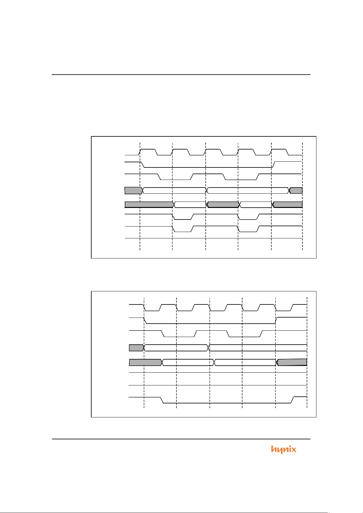
XIN
nCS
Address
nAS
Data
nHWR
nLWR
n
n + 2
Valid
Valid
nRD
‘1’
XIN
nCS
Address
nAS
Data
nHWR
nLWR
n
n + 2
nRD
‘1’
‘1’
Valid
Valid
BUS controller Flash MCU(HMS39C7092)
3.4.3 Basic Bus Control Signal Timing
16-Bit 1-Wait-Access Areas: Figure 3.5 shows the write timing of bus control
signals for a 16 -Bit 1-wait-access area (in case of 32 -bit word access). Figure 3.6
shows the read timing of bus control signals for a 16-Bit 1-wait-access area (In case
of 32-bit word access). In this case the NormWait value in BCR of this area is ‘0’.
Note: Sequential read access keeps nRD signal to LOW state.
n
Figure 3.5 Bus Control Signal Write Timing for 16-Bit, 1-Wait (Word Access)
n
Figure 3.6 Bus Control Signal Read Timing for 16-Bit, 1-Wait (Word Access)
56 Preliminary
Page 57
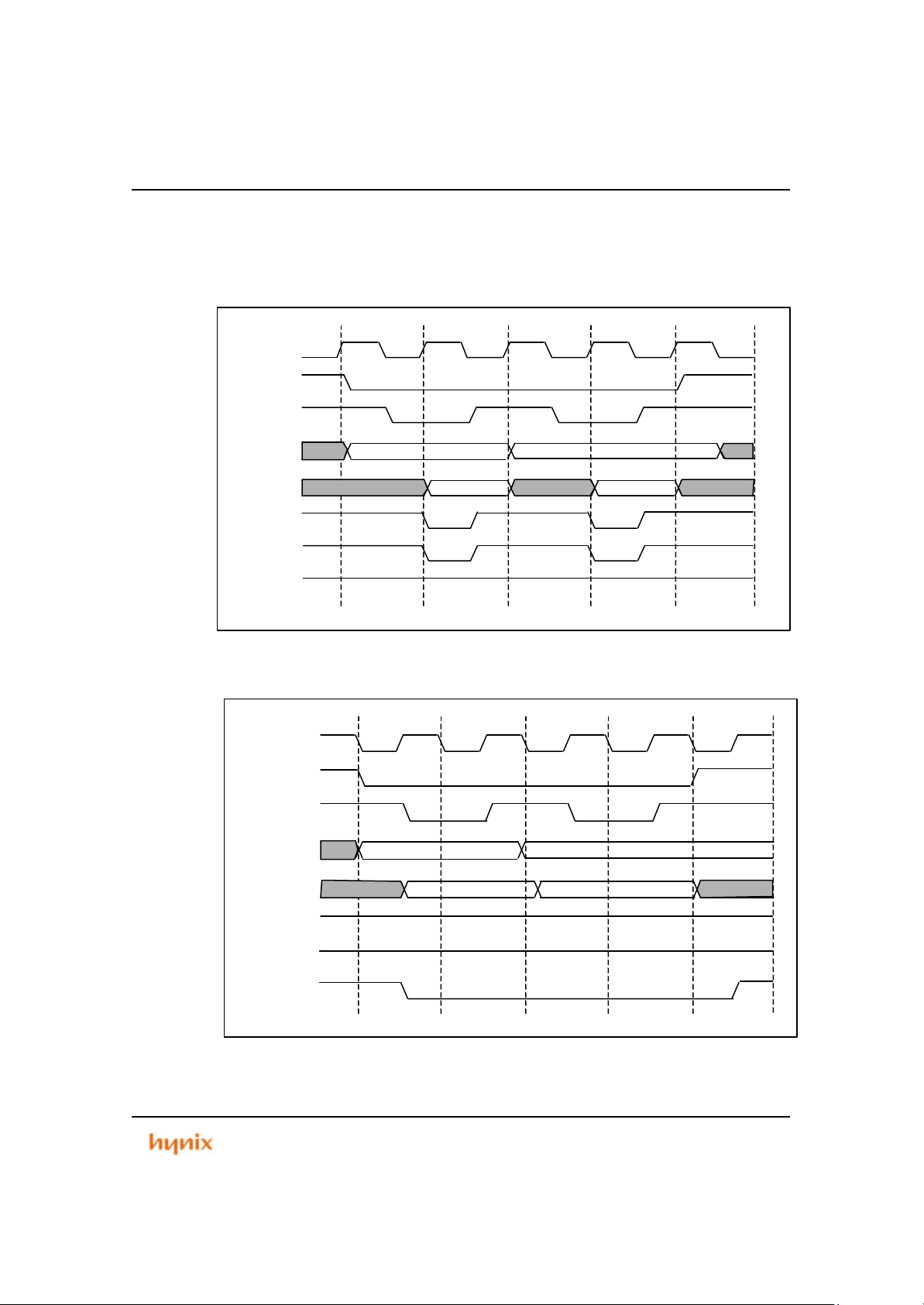
Address
nAS
nLWR
n
n + 2
nRD
‘1’
Address
nAS
nHWR
nLWR
n
n + 2
‘1’
‘1’
Flash MCU(HMS39C7092) BUS controller
Figure 3.7 shows the write timing of bus control signals for a 16-Bit 1-wait-access
area (In case of half-word access). Figure 3.8 shows the read timing of bus control
signals for a 16-Bit 1-wait-access area (In case of half-word access).
XIN
nCS
n
Data
nHWR
Valid Valid
Figure 3.7 Bus Control Signal Write Timing for 16-Bit, 1-Wait (Half-word Access)
XIN
nCS
n
Data
nRD
Valid
Valid
Figure 3.8 Bus Control Signal Read Timing for 16-Bit, 1-Wait (Half-word Access)
Preliminary 57
Page 58

Data
nLWR
n
nRD
‘1’
‘1’
XIN
nCS
Address
nAS
Data
nHWR
nLWR
n
nRD
Valid
BUS controller Flash MCU(HMS39C7092)
Figure 3.9 shows the write timing of bus control signals for a 16-Bit 1-wait-access
area (In case of byte access). Figure 3.10 shows the read timing of bus control
signals for a 16-Bit 1-wait-access area (In case of byte access).
XIN
nCS
n
nAS
Address
nHWR
Figure 3.9 Bus Control Signal Write Timing for 16-Bit, 1-Wait (Byte Access)
n
Valid
Figure 3.10 Bus Control Signal Read Timing for 16-Bit, 1-Wait (Byte Access)
58 Preliminary
Page 59

XIN
nCS
nAS
Data
nLWR
nRD
n
Valid
Valid
‘1’
Address
nAS
Data
nHWR
n
n + 2
‘1’
‘1’
Valid
Flash MCU(HMS39C7092) BUS controller
Figure 3.11 shows the write timing of bus control signals for a 16-Bit 2-wait-access
area (In case of word access). Figure 3.12 shows the read timing of bus control
signals for a 16-Bit 2-wait-access area (In case of word access).
n
Address
nHWR
n + 2
Figure 3.11 Bus Control Signal Write Timing for 16-Bit, 2-Wait (Word Access)
XIN
nCS
n
Valid
nLWR
nRD
Figure 3.12 Bus Control Signal Read Timing for 16-Bit, 2-Wait (Wo rd Access)
Preliminary 59
Page 60

XIN
nCS
nAS
Data
nLWR
n
Valid
nRD
‘1’
XIN
nCS
Address
nAS
Data
nHWR
nLWR
n
nRD
Valid
BUS controller Flash MCU(HMS39C7092)
Figure 3.13 shows the write timing of bus control signals for a 16-Bit 2-wait-access
area (In case of half-word access). Figure 3.14 shows the read timing of bus control
signals for a 16-Bit 2-wait-access area (In case of half -word access).
n
Address
nHWR
Figure 3.13 Bus Control Signal Write Timing for 16-Bit, 2-Wait (Half-Word Access)
n
Figure 3.14 Bus Control Signal Read Timing for 16-Bit, 2-Wait (Half-Word Access)
60 Preliminary
Page 61

nCS
Address
nAS
nLWR
n
nRD
‘1’
‘1’
XIN
nCS
nAS
n
Flash MCU(HMS39C7092) BUS controller
Figure 3.15 shows the write timing of bus control signals for a 16-Bit 2-wait-access
area (In case of byte access). Figure 3.16 shows the read timing of bus control
signals for a 16-Bit 2-wait-access area (In case of byte access).
XIN
n
Data
nHWR
Valid
Figure 3.15 Bus Control Signal Write Timing for 16-Bit, 2-Wait (Byte Access)
n
Address
Data
nHWR
nLWR
nRD
Figure 3.16 Bus Control Signal Read Timing for 16-Bit, 2-Wait (Byte Access)
Valid
Preliminary 61
Page 62

XIN
Address
Data
nHWR
nLWR
n
‘1’
‘1’
Valid
nWAIT
T1T2Tw
Tw
Tw
T3
BUS controller Flash MCU(HMS39C7092)
3.4.4 Wait Control
When accessing external space, the HMS39C7092 can extend the bus cycle by
inserting wait states (Tw). There are two ways of inserting wait states: (1) program
wait insertion and (2) pin wait insertion using the nWAIT pin.
Program Wait Insertion: From 1 to 16 wait states can be inserted automatically
between the T2 state and T3 state on an individual basis in each access space,
according to the settings of NormWait bit fields in BCR0~7.
Pin Wait Insertion: When external space is accessed in this state, a program wait is
first inserted. If the nWAIT pin is low at the falling edge of XIN in the last T2 or Tw
state, another Tw state is inserted. If the nWAIT pin is held low, Tw states are
inserted until it goes high.
Figure 3.17 shows an example of the timing for insertion of one program wait state in
3-wait-state space.
nCS
n
nAS
nRD
Figure 3.17 Example of Wait State Insertion Timing.
62 Preliminary
Page 63

Flash MCU(HMS39C7092) BUS controller
3.4.5 Bus Arbiter
The bus controller has a built-in bus arbiter that arbitrates between different bus
masters. The bus master can be either the CPU or an external bus master. When a
bus master has the bus right it can carry out read and write operations. Each bus
master uses a bus request signal to request the bus right. At fixed times the bus
arbiter determines priority and uses a bus acknowledge signal to grant the bus to a
bus master, which can operate using the bus.
The bus arbiter checks whether the bus request signal from a bus master is active or
inactive, and returns an acknowledge signal to the bus master. When two or more
bus masters request the bus, the highest-priority bus master receives an
acknowledge signal can continue to use the bus until the acknowledge signal is
deactivated.
The bus master priority order is:
(High) External bus master > ARM CPU (Low)
The bus arbiter samples the bus request signals and determines priority at all times,
but it does not always grant the bus immediately, even when it receives a bus request
a bus master with higher priority than the current bus master. Each bus master has
certain times at which it can release the bus to a higher-priority bus master.
ARM CPU: The ARM CPU is the lowest-priority bus master. If an external bus master
requests the bus while the CPU has the right, the bus arbiter transfers the bus right to
the bus master that requested it. The bus right is transferred at the following times:
l The bus right is transferred at the boundary of a bus cycle. If word data is
accessed by two consecutive byte accesses, however, the bus right is not
transferred between the two byte accesses.
l If another bus master requests the bus while the CPU is performing internal
operations, such as executing a multiply or divide instruction, the b us right
is transferred immediately. The CPU continues its internal operations.
l If another bus master requests the bus while the CPU is in power down
mode, the bus right is transferred immediately.
External Bus Master: The HMS39C7092 can be always release d to an external bus
master. The external bus master has highest priority, and requests the bus right from
the bus arbiter driving the nBREQ signal low. Once the external bus master acquires
the bus, it keeps the bus until the nBREQ signal goes to high. Wh ile the bus is
released to an external bus master, the HMS39C7092 chip holds the address bus,
data bus, bus control signals (nAS, nRD, nHWR, and nLWR ), and chip select signals
(nCS0 to 7), and holds the nBACK pin in the low output state.
The bus arbiter samples the nBREQ pin at the rise of the system clock (XIN). If
nBREQ is low, the bus is released to the external bus master at the appropriate
opportunity. The nBREQ signal should be held low until the nBACK goes low.
When the nBREQ pin is high in two consecutive samples, the nBACK pin is driven
high to end the bus-release cycle.
Preliminary 63
Page 64

nCS
nAS
nHWR
nLWR
nRD
‘1’
‘1’
Valid
Tw T3CPU Cycle
External Bus Cycle
nBREQ
nBACK
BUS controller Flash MCU(HMS39C7092)
Figure 3.18 shows the timing when the bus right is requested by an external bus
master during a read cycle in a 1-wait-state access area. There is a minimum interval
of three states from when the nBREQ signal goes low until the bus is released.
XIN
n
Address
Data
Figure 3.18 Example of External Bus Master Operation
T0 T1 T2 Tw
n
64 Preliminary
Page 65

Flash MCU(HMS39C7092) MCU controller
Chapter 4
MCU Controller
Preliminary 65
Page 66

MCU controller Flash MCU(HMS39C7092)
4.1 General Description
The MCU Controller (MCUC) is composed of 11 multi -function pin multiplex control
signal registers and device code register.
4.2 Pin Function Description
Table 4.1 shows Pin function description.
Table 4. 1 Pin Function Descriptions
NAME
Port A
Port B
Port 1
Port 2
Port 3
*XP96/XFVPPD pin is package bonding options
Note: Each port functions are changed by Mode-setting or user definition.
Default functions are showed in 4.3.2 PINMUX Register
Port
No.
PA0 TCLKA P40 D0
PA1 TCLKB P41 D1
PA2 TCLKC, TIOCA0 P42 D2
PA3 TCLKD, TIOCB0 P43 D3
PA4 A23, TIOCA1 P44 D4
PA5 A22, TIOCB1 P45 D5
PA6 A21, TIOCA2 P46 D6
PA7 A20, TIOCB2
PB0 nCS7, TIOCA3 P50 A16
PB1 nCS6, TIOCB3 P51 A17
PB2 nCS5, TUICA4 P52 A18
PB3 nCS4, TIOCB4
PB4 TMS P60 nWAIT
PB5 TDO P61 nBREQ
PB6 TDI P62 nBACK
PB7 TCK P63 nAS
P10 A0 P64 nRD
P11 A1 P65 nHWR
P12 A2 P66 nLWR
P13 A3
P14 A4 P70 AN0
P15 A5 P71 AN1
P16 A6 P72 AN2
P17 A7 P73 AN3
P20 A8 P74 AN4
P21 A9 P75 P75
P22 A10 P76 TIOCA5, nIRQ6
P23 A11
P24 A12 P80 nIRQ0
P25 A13 P81 nCS3, nIRQ1
P26 A14 P82 nCS2, nIRQ2
P27 A15 P83 nCS1, nIRQ3
P30 D8
P31 D9 P90 TxD0
P32 D10 P91 RxD0
P33 D11 P92 TxD1
P34 D12 P93 RxD1
P35 D13 XP96* XFVPPD*
P36 D14
P37 D15
Multiplexed functions NAME
Port 4
Port 5
Port 6
Port 7
Port 8
Port 9
Port
No.
P47 D7
P53 A19
P67 CLKO
P77 TIOCB5, nIRQ7
P84 nCS0
P97 nTRST
Multiplexed functions
66 Preliminary
Page 67

Flash MCU(HMS39C7092) MCU controller
4.3 Register Description
4.3.1 Register Memory Map
Table 4.2 is the memory map of the MCU Controller. The base address of MCU
control Register is 0x0900_0000. Table 4.3 shows the initial value in each mode. The
initial values are different by operation mode.
Table 4.2 Memory map of the MCU Controller
Reg.
PAMR 0x0000 R/W Pin MUX Control Register for Port A
PBMR 0x0004 R/W Pin MUX Control Register for Port B
P1MR 0x0008 R/W Pin MUX Control Register for Port 1
P2MR 0x000C R/W Pin MUX Control Register for Port 2
P3MR 0x0010 R/W Pin MUX Control Register for Port 3
P4MR 0x0014 R/W Pin MUX Control Register for Port 4
P5MR 0x0018 R/W Pin MUX Control Register for Port 5
P6MR 0x001C R/W Pin MUX Control Register for Port 6
P7MR 0x0020 R/W Pin MUX Control Register for Port 7
P8MR 0x0024 R/W Pin MUX Control Register for Port 8
P9MR 0x0028 R/W Pin MUX Control Register for Port 9
DCR 0x002C R MCU Device Code Register
Table 4.3 MCU Controller Initial values in each mode
Reg.
PAMR 0x0000 0x0000 0x1540 0x1540
PBMR 0x0000 0x0000 0x0055 0x0000
P1MR 0x0000 0x0000 0x00FF 0x0000
P2MR 0x0000 0x0000 0x00FF 0x0000
P3MR 0x00FF 0x0000 0x00FF 0x0000
P4MR 0x0000 0x0000 0x00FF 0x0000
P5MR 0x0000 0x0000 0x000F 0x0000
P6MR 0x0000 0x0000 0x03FF 0x0000
P7MR 0x0000 0x0000 0x0000 0x0000
P8MR 0x0000 0x0000 0x00D4 0x0000
P9MR 0x0000 0x0000 0x0000 0x0000
DCR 0x39437092 0x39437092 0x39437092 0x39437092
I/O
OFFSET
Mode
2
Dir. Description
Mode
3,4
MODE
5,7
MODE
6
Preliminary 67
Page 68

MCU controller Flash MCU(HMS39C7092)
4.3.2 PINMUX Register
PAMR Port A Multiplex Register (0x0900_0000 R/W)
b31 b14 b13 b12 b11 b10 b9 b8 b7 b6 b5 b4 b3 b2 b1 b0
PAMR
PBMR Port B Multiplex Register (0x0900_0004 R/W)
b31 b14 b11 b10 b9 b8 b7 b6 b5 b4 b3 b2 b1 b0
PBMR
Reserved PA7 PA6 PA5 PA4 PA3 PA2 PA1 PA0
Initial value : depend on operating mode (refer to Table 4.3)
PA7 00 : A20 01 : TIOCB2
1x : PA7
PA6 00 : A21 01 : TIOCA2
1x : PA6
PA5 00 : A22 01 : TIOCB1
1x : PA5
PA4 00 : A23 01 : TIOCA1
1x : PA4
PA3 00 : TCLKD 01 : TIOCB0
1x : PA3
PA2 00 : TCLKC 01 : TIOCA0
1x : PA2
PA1 0 : TCLKB 1 : PA1
PA0 0 : TCLKA 1 : PA2
Reserved PB7 PB6 PB5 PB4 PB3 PB2 PB1 PB0
Initial value : depend on operating mode (refer to Table 4.3)
PB7 0 : TCK 1 : PB7
PB6 0 : TDI 1 : PB6
PB5 0 : TDO 1 : PB5
PB4 0 : TMS 1 : PB4
PB3 00 : /CS4 01 : TIOCB4
1x : PB3
PB2 00 : /CS5 01 : TIOCA4
1x : PB2
PB1 00 : /CS6 01 : TIOCB3
1x : PB1
PB0 00 : /CS7 01 : TIOCA3
1x : PB0
68 Preliminary
Page 69

Flash MCU(HMS39C7092) MCU controller
P1MR Port 1 Multiplex Register (0x0900_0008 R/W)
b31 b8 b7 b6 b5 b4 b3 b2 b1 b0
P1MR
Initial value : depend on operating mode (refer to Table 4.3)
P17 0 : A7 1 : P17
P16 0 : A6 1 : P16
P15 0 : A5 1 : P15
P14 0 : A4 1 : P14
P13 0 : A3 1 : P13
P12 0 : A2 1 : P12
P11 0 : A1 1 : P11
P10 0 : A0 1 : P10
P2MR Port B Multiplex Register (0x0900_000C R/W)
b31 b8 b7 b6 b5 b4 b3 b2 b1 b0
P2MR
Initial value : depend on operating mode (refer to Table 4.3)
P27 0 : A15 1 : P27
P26 0 : A14 1 : P26
P25 0 : A13 1 : P25
P24 0 : A12 1 : P24
P23 0 : A11 1 : P23
P22 0 : A10 1 : P22
P21 0 : A9 1 : P21
P20 0 : A8 1 : P20
P3MR Port 3 Multiplex Register (0x0900_0010 R/W)
b31 b8 b7 b6 b5 b4 b3 b2 b1 b0
P3MR
Initial value : depend on operating mode (refer to Table 4.3)
P37 0 : D8 1 : P37
P36 0 : D9 1 : P36
P35 0 : D10 1 : P35
P34 0 : D11 1 : P34
P33 0 : D12 1 : P33
P32 0 : D13 1 : P32
P31 0 : D14 1 : P31
P30 0 : D15 1 : P30
Reserved P17 P16 P15 P14 P13 P12 P11 P10
Reserved P27 P26 P25 P24 P23 P22 P21 P20
Reserved P37 P36 P35 P34 P33 P32 P31 P30
Preliminary 69
Page 70

MCU controller Flash MCU(HMS39C7092)
P4MR Port 4 Multiplex Register (0x0900_0014 R/W)
b31 b8 b7 b6 b5 b4 b3 b2 b1 b0
P4MR
Initial value : depend on operating mode (refer to Table 4.3)
P47 0 : D7 1 : P47
P46 0 : D6 1 : P46
P45 0 : D5 1 : P45
P44 0 : D4 1 : P44
P43 0 : D3 1 : P43
P42 0 : D2 1 : P42
P41 0 : D1 1 : P41
P40 0 : D0 1 : P40
P5MR Port 5 Multiplex Register (0x0900_0018 R/W)
b31 b4 b3 b2 b1 b0
P5MR
Initial value : depend on operating mode (refer to Table 4.3)
P53 0 : A19 1 : P53
P52 0 : A18 1 : P52
P51 0 : A17 1 : P51
P50 0 : A16 1 : P50
P6MR Port 6 Multiplex Register (0x0900_001C R/W)
b31 b10 b9 b8 b7 b6 b5 b4 b3 b2 b1 b0
P6MR
Initial value : depend on operating mode (refer to Table 4.3)
P66 0 : /LWR 1 : P66
P65 0 : /HWR 1 : P65
P64 0 : /RD 1 : P64
P63 0 : /AS 1 : P63
P67 0 : BCLK 1 : P67
P62 00 : /BACK 01 : P62
1x : Reserved
P61 00 : /BREQ 01 : P61
1x : Reserved
P60 0 : /WAIT 1 : P60
Reserved P47 P46 P45 P44 P43 P42 P41 P40
Reserved P53 P52 P51 P50
Reserved P66 P65 P64 P63 P67 P62 P61 P60
70 Preliminary
Page 71

Flash MCU(HMS39C7092) MCU controller
P7MR Port 7 Multiplex Register (0x0900_0020 R/W)
b31 b9 b8 b7 b6 b5 b4 b3 b2 b1 b0
P7MR
P8MR Port 8 Multiplex Register (0x0900_0024 R/W)
b31 b8 b7 b6 b5 b4 b3 b2 b1 b0
P8MR
P9MR Port 9 Multiplex Register (0x0900_0028 R/W)
b31 b11 b10 b9 b8 b7 b6 b5 b4 b3 b2 b1 b0
P9MR
Reserved P77 P76 P74 P73 P72 P71 P70
Initial value : depend on operating mode (refer to Table 4.3)
P77 00 : TIOCB5 01 : /IRQ7
1x : P77
P76 00 : TIOCA5 01 : /IRQ6
1x : P76
P74 0 : AN4 1 : P74
P73 0 : AN3 1 : P73
P72 0 : AN2 1 : P72
P71 0 : AN1 1 : P71
P70 0 : AN0 1 : P70
Reserved P84 P83 P82 P81 P80
Initial value : depend on operating mode (refer to Table 4.3)
P84 0 : /CS0 1 : P84
P83 00 : /CS1 01 : /IRQ3
1x : P83
P82 00 : /CS2 01 : /IRQ2
1x : P82
P81 00 : /CS3 01 : /IRQ1
1x : P81
P80 0 : /IRQ0 1 : P80
Reserved P97 P95 P94 P93 P92 P91 P90
Initial value : depend on operating mode (refer to Table 4.3)
P97 0 : /TRST 1 : P97
P95 00 : /IRQ5 01 : P95
1x : Reserved
P94 00 : /IRQ4 01 : P94
1x : Reserved
P93 00 : /RxD1 01 : P93
1x : Reserved
P92 00 : /TxD1 01 : P92
1x : Reserved
P91 0 : RxD0 1 : P91
P90 0 : TxD0 1 : P90
Preliminary 71
Page 72

MCU controller Flash MCU(HMS39C7092)
4.3.3 MCU Device Code Register (0x0900_002C Read Only)
This Register is read only. Device Code Value is ‘0x3943_7092’
72 Preliminary
Page 73

Flash MCU(HMS39C7092) Power Management Unit
Chapter 5
Power Management Unit
Preliminary 73
Page 74

Register
RESET Filter
Generator
PMU State Machine
MODE
1/2
RESET Filter
XnRES
MODE[2:0]
XTALOUT
XTALIN
SCLK_GEN
CLKIN
SCLK
BCLK
MUX
XCLKOUT
Module Clock
RES_OUT
0
MUX
WDT_Overflow
nFIQ Interrupt
nIRQ Interrupt
Power Management Unit Flash MCU(HMS39C7092)
5.1 General Description
The PMU block provides:
• Clock distribution of all over system
• Reset, RUN and Power down modes control
TEST
Clock Control
RESET
Figure 5.1 PMU Block Diagram
PIN
MUX
Internal System
Internal Blocks
PIN
MUX
RESET
INTC
TIMER
WDT
UART0,1
ADC
74 Preliminary
Page 75

Flash MCU(HMS39C7092) Power Management Unit
5.2 Operation Modes
5.2.1 Introduction
The PMU is consisted of clock controller and reset controller. User can control
internal clocks those are embedded peripherals and main clock of MCU by setting
the registers of PMU. The MCU has three reset sources those are external power-on
reset, soft-reset of PMU, soft-reset of WDT and overflow reset of WDT. And PMU has
status registers that old reset value and PMU status.
To improve power management, support for a power-saving mode where bus clocks
may be disabled (or dropped to lower clock) is included.
The reset and power-down mechanism provides:
• Stable power-up sequence
• Power On Reset
• Soft Reset
Additionally a system bus, once operational, benefits from well-defined modes of
operation:
• RUN
• Power-down mode
5.2.2 Reset and Operation Modes
A set of four use ful states or modes is defined as follows:
RESET
When it is power-on, watchdog timer overflow, watchdog soft-reset or PMU soft-reset,
the MCU is initialized
Power on Reset
This state should be forced by any on-chip power-on-reset cell or external power-on
signal and maintained until bus clock is safe and stable.
The POR is forced to be in an asynchronous start-up condition and must be
recognized by all master and slave devices to disable output drives (and wait for a
valid clock). The MCU is running after 32 clocks end of reset timing that rising edge
of reset signal.
Soft- Reset of PMU
The soft-reset, which may need to apply to allow all soft resetting of the bus for a
number of clock cycles. In this reset states the PMU block initializes all the ASB
blocks, Bus controller, DRAM Controller, DMA Controller, ARM CPU core, and Arbiter,
Decoder.
Preliminary 75
Page 76

Reset
Wake-up
by Interrupt
(nFIQ or nIRQ)
Soft-Reset
Wake-up
by Power-On Reset
Power Management Unit Flash MCU(HMS39C7092)
Overflow and Soft-Reset of Watchdog timer
The watchdog timer can generate reset signal, when timer overflows or sets the
register value. Detailed information are in the watchdog timer manual, please refer to
it.
PDN – Power-Down Mode
When MCU system is in the PDN State, PMU block disables all of the blocks in the
ASB and APB, so the power consumption of system is dramatically low. Although
MCU is in the power down mode, user can set interrupt controller block working in
the power down mode.
Wake-up from the PDN Mode.
The Wake-up is a temporal state for wake-up from power down state through the
interruption. After wake-up state, next state becomes RUN state automatically.
WDT_Overflow
Reset
Power-On
RESET
WDT, PMU
RUN
Figure 5.2 Reset and Power Management State Machine.
Power Down
PMU
Command
76 Preliminary
Page 77

Flash MCU(HMS39C7092) Power Management Unit
5.3 Power Management Unit Register Map
The start address of the PMU(Power Management Unit) is 0x0900_1000.
Table 5.1 Register Map of the PMU
Name I/O Offset DIR Description
PMUCR 0x1000 W PMU operation mode controls register.
PMUSR 0x1000 R PMU status register shows the just previous
PCLKCR 0x1008 R/W Peripheral clock control register .
MEMSR 0x100C R Memory remap status register.
MEMCR 0x1010 W Memory remap control register
RSTCR 0x1030 W Soft-Reset control register
PMU state.
Preliminary 77
Page 78

Power Management Unit Flash MCU(HMS39C7092)
5.4 Register Description
The PMU supplies the clock to all of the blocks in the MCU. The start address of
register is 0x0900_1000.
PMUCR PMU Control Register (0x0900_1000 Write-Only)
b31 - b8 b7 b6 b5 b4 b3 b2 b1 b0
PMUCR Reserved PD
Reset - 0 0 0 0 0 0 0 0
Initial value : 0x -00
PD 11 : Entering the Power down Mode
This register controls the operation mode of PMU. When power on reset states,
register value is initialized by Run State (00). If PMUCR is 3, device enters the
PD(Power Down) mode. The other values don’t effect. The address of register is
0x0900_1000.
PMUST PMU Status Register (0x0900_1000 Read -Only)
b31 - b8 b5 b4 b3 b2 b1 b0
PMUST Reserved PMUST Reserved PMUST
Reset - 0 0 - 0 0
Initial value : 0x -00
This register holds the previous status and reset state of PMU. The address of
register is 0x0900_1000.
00 : Clear PMU Status Register
PMUST (Previous Reset Status bits)
00 – The Power-On reset state (nPOR)
01 – PMU Soft-reset state
10 – WDT Soft-reset state
11 – WDT Overflow-reset state
PMUST (PMU Status bits)
00 – Start after Power-On reset
01 – reserved state
10 – reserved state
11 – Start after Power-Down mode
78 Preliminary
Page 79

Flash MCU(HMS39C7092) Power Management Unit
PCLKCR Clock Control Register (0x0900_1008 R/W)
b31 - b16 b15 b14 b13 b12 b11 b10 b9 b8 b7 b6 B5 b4 b3 b2 b1 b0
PCLKCR Reserved WU_SEL INTC_CC WDT_CC UART_Clk UART_CC TIMER_CC ADC_CC
Reset - 0 0 0 0 0 0 0 0 0 0 0 0 0 0 0 0
Initial value : 0x 00000000
The address of register is 0x0900_1008.
WU_SEL : Wake-up source interrupt select register
0 - MCU wake-up when nFIQ interrupt occurr
1 - MCU wake-up when nIRQ interrupt occurr
INTC_CC : Interrupt controller clock control register
0 - Interrupt controller use the XIN clock. XIN is not killed at any
mode
1 - Interrupt controller use the BCLK of internal Bus clock. The
WDT_CC : Clock control register of WDT
000 - BCLK
001 - BCLK/2
010 ~ 111 – Reserved
UART_Clk : UART0, 1 clocks on-off control register.
00 - UART0,1 clocks ON
01 - UART1 clock ON, UART0 clock OFF
10 - UART1 clock OFF, UART0 clock ON
11 – UART0,1 clocks OFF
UART_CC : Clocks Control register of UART.
000 - BCLK
001 - BCLK/2
010 ~ 111 – Reserved
TIMER_CC : Clocks Control register of TIMER.
000 - BCLK
001 - BCLK/2
010 ~ 111 – Reserved
ADC_CC : Clocks Control register of ADC.
Values are same as WDT_CC
Bus clock is killed when Power-down mode
Preliminary 79
Page 80

Power Management Unit Flash MCU(HMS39C7092)
MEMCR Memory map Control Register (0x0900_1010 Write-Only)
MEMSR Memory map Status Register (0x0900_100C Read -Only)
b31 - b3 b2 b1 b0
MEMCR
MEMSR
Reset - 0 0 0
RSTCR Soft-Reset Control Register (0x0900_1030 R/W)
b31 - b1 b0
RSTCR Reserved RSTCR
Reset - 0
Reserved SM On-Flash REMAP
Initial value : 0x -0
In write operation, the address of register is 0x0900_1010 and in read operation,
the address of register is 0x0900_100C.
SM : External bus controller mapping change.
0 - Each nCS0 ~ nCS7 of address space is 16MB
size
1 - Each nCS0 ~ nCS7 of address space is 1MB
size
On-Flash : Re-mapping of Flash start address to 0x0 in MODE
6 and 7.
0 - Default value.
1 - Re-mapping of Flash start address to 0x0 in the
memory map. It is valid at MODE 6 and 7.
REMAP : Re-map internal SRAM address location.
0 - Default value.
1 – Re-mapping of internal SRAM start address to
0x0 in the memory map. It is used at MODE
2,3,4,5,6 and 7.
Initial value : 0x -0
RSTCR 1 : Normal reset
0 : Normal
This register is used for generating the Soft-reset operation. The MCU is entered in
reset state, when this register is set to high, it is cleared automatically at the end of
Soft-Reset procedure. The address is 0x 0900_1030.
80 Preliminary
Page 81

Flash MCU(HMS39C7092) Power Management Unit
5.5 Signal Timing Diagram
The PMU signal timing is as shown below.
5.5.1 Power on Reset
5.5.2 Watch Dog Timer Overflow
CLKIN
XnRES
32 clks
BnRES
Figure 5.3 Power on Reset Timing Diag ram
BCLK
WD_OF_IN
WD_OF_OUT 256 clks
BnRES
Figure 5.4 Watch Dog Timer Overflow Timing Diagram
512 clks
Preliminary 81
Page 82
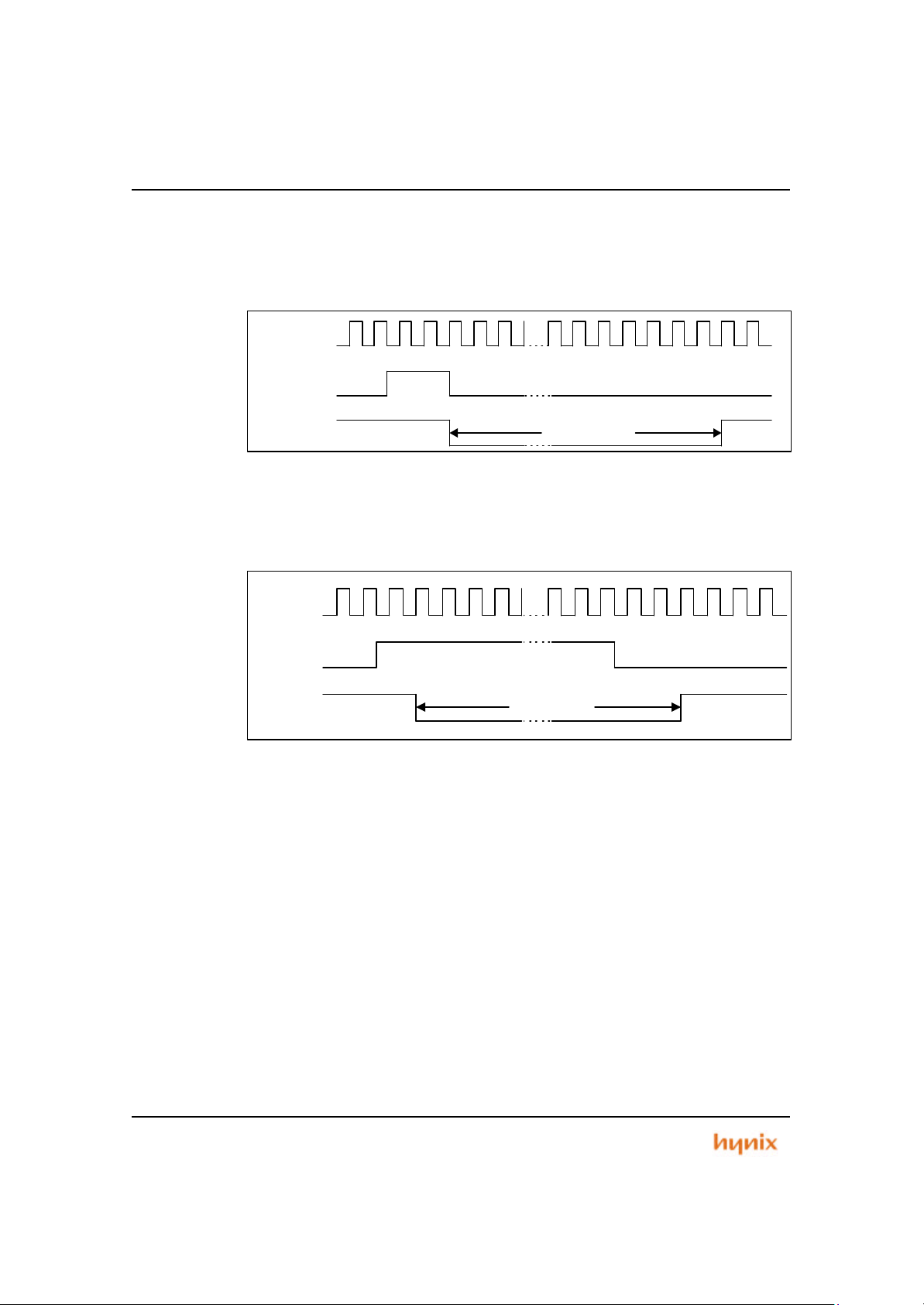
Power Management Unit Flash MCU(HMS39C7092)
5.5.3 Soft-Reset
There are two Soft-Reset cases. The first Soft-Reset operation is switched by
MAN_RST signal from WDT.
Another case is from PMU reset control register.
BCLK
MAN_RST
BnRES 512 clks
Figure 5.5 Soft Reset (from WDT) Timing Diagram
BCLK
RSTCR
BnRES
Figure 5.6 Soft Reset (from PMU) Timing Diagram
512 clks
82 Preliminary
Page 83

Flash MCU(HMS39C7092) Interrupt controller
Chapter 6
The Interrupt Controller
Preliminary 83
Page 84

Control
Control
Control
Control
21 21
Interrupt controller Flash MCU(HMS39C7092)
6.1 About the Interrupt controller
The interrupt controller has the following features :
• Asynchronous interrupt controller
• 8 external interrupt sources
• 13 internal interrupt sources
• Low interrupt s latency
• Selection of the active modes of all interrupt s source inputs
(Level or Edge trigger)
• Mask-able for each interrupt source and output signal
• Selection of the output paths (IRQ or FIQ for each interrupt source)
IRQ source0
IRQ source1
IRQ source2
IRQ source3
IRQ source4
IRQ source5
Source Mask
Trigger Mode
Polarity
Direction
Status
Control
FIQ
Request
Control
FIQ
Mask
nFIQ
High/
Low,
Rising/
Falling
Control
Clear Control
FIQ
or
IRQ
21
IRQ
21
21
IRQ source15
IRQ source16
IRQ source17
IRQ source18
IRQ source19
IRQ source20
Mask
Control
21
Edge/
Level
Control
Figure 6.1 Interrupt Control Flow Diagram
84 Preliminary
IRQ
Mask
nIRQ
Page 85

Flash MCU(HMS39C7092) Interrupt controller
6.1.1 Interrupt sources
The interrupt controller provides interface between multiple interrupt sources and the
processor. The interrupt controller supports internal and external interrupt sources.
Internally there are 11 peripheral interrupt sources. Externally there are 8 interrupt
sources. Therefore certain interrupt bits can be defined for the basic functionality
required in any system, while the remaining bits are available for use by other
devices in any particular implementation.
Table 6.1 Interrupt Controller Default Setting Value
Interrupt No. INTERRUPT SOURCES
INT0 External Int errupt 0
INT1 External Interrupt 1
INT2 External Interrupt 2
INT3 External Interrupt 3
INT4 External Interrupt 4
INT5 External Interrupt 5
INT6 External Interrupt 6
INT7 External Interrupt 7
INT8 reserved
INT9 reserved
INT10 WDT
INT11 UART0
INT12 UART1
INT13 ADC
INT14 Timer 0
INT15 Timer 1
INT16 Timer 2
INT17 Timer 3
INT18 Timer 4
INT19 Timer 5
INT20 Software Interrupt
The Users can set the active mode of all interrupt source inputs. The default mode is
the falling -edge trigger mode. Any inversion or latching required to providing edge
sensitivity must be provided at the generating source of the interrupt.
No hardware priority scheme or any form of interrupt vectoring is provided, but the
priority can be determined using FIQ mask regis ter and IRQ mask register under
software control.
FIQ mask register and IRQ mask register are also provided to generate an interrupt
under software control. Typically these registers may be used to determine either a
FIQ interrupt or an IRQ interrupt.
6.1.2 Interrupt Control
The interrupt controller provides the interrupt source status and the interrupt request
status. The interrupt mask register s are used to determine whether an active interrupt
source should generate an interrupt request to the process or or not. A logic-level
HIGH in the interrupt mask register indicates that the interrupt source is masked and
then doesn‘t generate a request.
FIQ mask register and IRQ mask register indicate whether the interrupt source
caus es a processor interrupt or not.
Preliminary 85
Page 86

Interrupt controller Flash MCU(HMS39C7092)
The interrupt modes are configurable by interrupt trigger mode register and interrupt
trigger polarity register. And Interrupt direction register indicates whether each
interrupt source drives IRQ or FIQ.
The FIQ and IRQ status register is used to refl ect the status of all channels set to
produce an FIQ interrupt or IRQ interrupt. And the status registers are cleared by
writing ‘1’ to the status clear register in the edge trigger mode only.
Bit 20 is used as a software interrupt source. When source mask control register bit
20 is HIGH, an interrupt request occurs. To disable the software interrupt, Source
Mask Control Register bit 20 should be Low. Software interrupt source input is fixed
active HIGH and level sensitive.
86 Preliminary
Page 87

b14
b14
Flash MCU(HMS39C7092) Interrupt controller
6.2 Interrupt Controller Registers
The start address of the interrupt controller is 0x0900_1200. The offset of any
particular register from the start address is fixed. The following registers are
provided for both FIQ and IRQ interrupt controllers:
Table 6.2 Memory Map of the Interrupt Controller
REG. I/O OFFSET
GMR
TMR 0x1204 R/W Trigger Mode Register
TPR 0x1208 R/W Trigger Polarity Register
IDR 0x120C R/W Interrupt Direction Register
FSR 0x1210 R FIQ Status Register
ISR 0x1214 R IRQ Status Register
FMR 0x1218 R/W FIQ Mask Register
IMR 0x121C R/W IRQ Mask Register
ISCR 0x1220 W Interrupt Status Clear Register
GMR Global Mask Register (0x0900_1200 R/W)
b31 - b25 b24b23b22b21b20b19b18b17b16b15
GMR Reserved I24 I23 I22 I21 I20 I19 I18 I17 I16 I15 I14 I13 I12 I11 I10 I9 I8 I7 I6 I5 I4 I3 I2 I1 I0
Reset 0000000 1 1 1 1 1 1 1 1 1 1 1 1 1 1 1 1 1 1 1 1 1 1 1 1 1
Initial value : 0x 01FFFFF Bit field I0-I24 1 : Mask
0 : Unmask
The interrupt mask register is used to mask the interrupt input sources and defines
which active sources will generate an interrupt request to the processor. If certain bits
within the interrupt controller are not implemented, the corresponding bits in the
interrupt mask register must be masked. A bit value 0 indicates that the interrupt is
unmasked and will allow an interrupt request to reach the processor. A bit value 1
indicates that the interrupt is masked. Once a bit is masked, the corresponding bit in
the status register is cleared. On reset, all interrupt input -sources are masked.
TMR Trigger Mode Register (0x0900_1204 R/W)
b31 - b25 b24b23b22b21b20b19b18b17b16b15
TMR Reserved I24 I23 I22 I21 I20 I19 I18 I17 I16 I15 I14 I13 I12 I11 I10 I9 I8 I7 I6 I5 I4 I3 I2 I1 I0
Reset 0000000 1 0 0 0 0 0 0 0 0 0 0 0 0 0 0 0 0 0 0 0 0 0 0 0 0
Initial value : 0x 0100000 Bit field I0-I24 1 : Level Trigger Mode
0 : Edge Trigger Mode
The interrupt trigger mode register is used to configure the interrupts with the
interrupt trigger polarity register. Each interrupt can be configured to level or edge
triggered. A bit value 0 indicates that the interrupt is configured to edge triggered and
a bit value 1 indicates that the interrupt is configured to level triggered. On reset, all
interrupt input sources are configured to edge triggered.
0x1200 R/W Global Mask Register
Dir Description
b13b12b1 1 b10 b9 b8 b7 b6 b5 b4 b3 b2 b1 b0
b13b12b11 b10 b9 b8 b7 b6 b5 b4 b3 b2 b1 b0
Preliminary 87
Page 88

b14
Interrupt controller Flash MCU(HMS39C7092)
TPR Trigger Polarity Register (0x0900_1208 R/W)
b31 - b25 b24b23b22b21b20b19b18b17b16b15b14b13b12b11 b10 b9 b8 b7 b6 b5 b4 b3 b2 b1 b0
TPR Reserved I24 I23 I22 I21 I20 I19 I18 I17 I16 I15 I14 I13 I12 I11 I10 I9 I8 I7 I6 I5 I4 I3 I2 I1 I0
Reset 0000000 1 0 0 0 0 0 0 0 0 0 0 0 0 0 0 0 0 0 0 0 0 0 0 0 0
Initial value : 0x 01000000 Bit field I0-I24 1 : High/Rising Edge
0 : Low/Falling Edge
The interrupt trigger polarity register is used to configure the interrupts with the
interrupt trigger mode register. Each interrupt can be configured to rising/high or
falling/low active. A bit value 0 indicates that the interrupt is configured to falling
active for edge trigger mode and to low active for level trigger mode. A bit value 1
indicates that the interrupt is configured to rising active for edge trigger mode and to
high active for level trigger mode. On reset, all interrupt input sources are configured
to falling/low active.
Table 6.3 Interrupt Source Trigger Mode
DETECTION MODE TMR TPR
Falling-Edge (Default) 0 0
Rising-Edge 0 1
Low-Level 1 0
High-Level 1 1
IDR Interrupt Direction Reg ister (0x0900_120C R/W)
b31 - b25 b24b23b22b21b20b19b18b17b16b15
IDR Reserved I24 I23 I22 I21 I20 I19 I18 I17 I16 I15 I14 I13 I12 I11 I10 I9 I8 I7 I6 I5 I4 I3 I2 I1 I0
Reset 0000000 0 0 0 0 0 0 0 0 0 0 0 0 0 0 0 0 0 0 0 0 0 0 0 0 0
Initial value : 0x 00000000 Bit field I0-I24 1 : Direction to FIQ
0 : Direction to IRQ
The interrupt direction register is used to determine whether each interrupt source
drives IRQ or FIQ. A bit value 0 indicates that the interrupt is driven to IRQ and a bit
value 1 indicates that the interrupt is driven to FIQ. On reset, all interrupt input
sources drive IRQ.
b13b12b11 b10 b9 b8 b7 b6 b5 b4 b3 b2 b1 b0
88 Preliminary
Page 89

b14
b14
b14
Flash MCU(HMS39C7092) Interrupt controller
FSR FIQ Status Register (0x0900_1210 Read Only)
b31 - b25 b24b23b22b21b20b19b18b17b16b15
FSR Reserved I24 I23 I22 I21 I20 I19 I18 I17 I16 I15 I14 I13 I12 I11 I10 I9 I8 I7 I6 I5 I4 I3 I2 I1 I0
Reset 0000000 0 0 0 0 0 0 0 0 0 0 0 0 0 0 0 0 0 0 0 0 0 0 0 0 0
Initial value : 0x 00000000 Bit field I0-I24 1 : FIQ Pending
0 : FIQ Idle
The FIQ status register is used to reflect the status of all channels set to produce an
FIQ interrupt (IDRn = 1). When an interrupt is set for an FIQ occurring, the
corresponding bit is set in FIQ status register. The interrupt handler will examine this
register to determine the channel(s) that caused the FIQ interrupt. When the status
clear register is written to ‘1’, the corresponding bit is cleared if that channel is
configured to edge trigger mode. A HIGH bit indicates that the interrupt is active and
will generate an interrupt to the processor.
ISR IRQ Status Register (0x0900_1214 Read Only)
b31 - b25 b24b23b22b21b20b19b18b17b16b15
ISR Reserved I24 I23 I22 I21 I20 I19 I18 I17 I16 I15 I14 I13 I12 I11 I10 I9 I8 I7 I6 I5 I4 I3 I2 I1 I0
Reset 0000000 0 0 0 0 0 0 0 0 0 0 0 0 0 0 0 0 0 0 0 0 0 0 0 0 0
Initial value : 0x 00000000 Bit field I0-I24 1 : IRQ Pending
0 : IRQ Idle
The IRQ status register is used to reflect the status of all channels set to produce an
IRQ interrupt (IDR(i) = 0). When an interrupt is set for an IRQ occurring, the
corresponding bit is set in IRQ status register. The interrupt handler will examine this
register to determine the channel(s) that caused the IRQ interrupt. When the status
clear register is written to ‘1’, the corresponding bit is cleared if that channel is
configured to edge trigger mode. A HIGH bit indicates that the interrupt is active and
will generate an interrupt to the processor.
FMR FIQ Mask Register (0x0900_1218 R/W)
b31 - b25 b24b23b22b21b20b19b18b17b16b15
FMR Reserved I24 I23 I22 I21 I20 I19 I18 I17 I16 I15 I14 I13 I12 I11 I10 I9 I8 I7 I6 I5 I4 I3 I2 I1 I0
Reset 0000000 0 0 0 0 0 0 0 0 0 0 0 0 0 0 0 0 0 0 0 0 0 0 0 0 0
Initial value : 0x 00000000 Bit field I0-I24 1 : Disable FIQ
0 : Enable FIQ
The FIQ request mask register is used to mask the request to generate an interrupt
to a processor. If certain bits within the interrupt controller are not implemented, the
corresponding bits in the FIQ reques t mask register must be masked. A bit value 0
indicates that the interrupt is unmasked and will allow an interrupt request to reach
the processor. A bit value 1 indicates that the interrupt is masked. On reset, all FIQ
requests are unmasked.
b13b12b11 b10 b9 b8 b7 b6 b5 b4 b3 b2 b1 b0
b13b12b11 b10 b9 b8 b7 b6 b5 b4 b3 b2 b1 b0
b13b12b11 b10 b9 b8 b7 b6 b5 b4 b3 b2 b1 b0
Preliminary 89
Page 90

b14
b14
Interrupt controller Flash MCU(HMS39C7092)
IMR IRQ Mask Register (0x0900_121C R/W)
b31 - b25 b24b23b22b21b20b19b18b17b16b15
IMR Reserved I24 I23 I22 I21 I20 I19 I18 I17 I16 I15 I14 I13 I12 I11 I10 I9 I8 I7 I6 I5 I4 I3 I2 I1 I0
Reset 0000000 0 0 0 0 0 0 0 0 0 0 0 0 0 0 0 0 0 0 0 0 0 0 0 0 0
Initial value : 0x 00000000 Bit field I0-I24 1 : Disable IRQ
0 : Enable IRQ
The IRQ request mask register is used to mask the request to generate an interrupt
to a processor. If certain bits within the interrupt controller are not implemented, the
corresponding bits in the IRQ request mask register must be masked. A bit value 0
indicates th at the interrupt is unmasked and will allow an interrupt request to reach
the processor. A bit value 1 indicates that the interrupt is masked. On reset, all IRQ
requests are unmasked.
ISCR Interrupt Status Clear Register (0x0900_1220 Write Only)
b31 - b25 b24b23b22b21b20b19b18b17b16b15
ISCR Reserved I24 I23 I22 I21 I20 I19 I18 I17 I16 I15 I14 I13 I12 I11 I10 I9 I8 I7 I6 I5 I4 I3 I2 I1 I0
Reset 0000000 0 0 0 0 0 0 0 0 0 0 0 0 0 0 0 0 0 0 0 0 0 0 0 0 0
Initial value : 0x 00000000 Bit field I0-I24 1 : Clear Interrupt Status
0 : No action
The status clear register is used to clear bits in the status register configured to the
edge trigger mode. If the channels are configured to the level trigger mode, the
corresponding bits in the FIQ status register and the IRQ status register have no
effect. This register is cleared when this register is written to ‘1’. When writing to this
register, each data bit that is HIGH causes the corresponding bit in the status register
to be cleared. Data bits that are LOW have no effect on the corresponding bit in the
status register. Note that the status clear register has an effect on the status register
in the edge trigger mode.
b13b12b11 b10 b9 b8 b7 b6 b5 b4 b3 b2 b1 b0
b13b12b11 b10 B9 b8 b7 b6 b5 B4 b3 b2 b1 b0
90 Preliminary
Page 91

Flash MCU(HMS39C7092) Watchdog Timer
Chapter 7
Watchdog Timer
Preliminary 91
Page 92

Watchdog Timer Flash MCU(HM S39C7092)
7.1 General Description
The watchdog timer has:
• watchdog timer mode and interval timer mode
• interrupt signal INT_WDT to interrupt controller in the watchdog timer mode &
interval timer mode
• output signal PORESET and MNRESET to PMU(Power Management Unit)
• eight counter clock sources
• selection whether to reset the chip internally or not
• two types of reset signal : power-on reset and manual reset
System Clock
PORST
INT_WDT
MNRST
Figure 7.1 Watchdog Timer Module Block Diagram
Clock
Generation
Reset
Control
Control Logic
Overflow
RSTSR
Module data bus
TCNT : Timer Counter (8-bit)
TRCR : Timer/Reset Control Register (8-bit)
RSTSR : Reset Status Register (2-bit)
Clock
Selection
Interrupt
Control
TCNT
Clock
TRCR
Bus
Interface
Internal
Signals
92 Preliminary
Page 93

Flash MCU(HMS39C7092) Watchdog Timer
7.2 Watchdog Timer Introduction
The HMS39C7092 has a one-channel watchdog timer(WDT) for monitoring system
operations. If a system becomes uncontrolled and the timer counter overflows without
being rewritten correctly by the CPU, an reset signal is output to PMU.
When this watchdog function is not needed, the WDT can be used as an interval
timer. In the interval timer operation, an interval timer interrupt is generated at each
counter overflow.
The WDT has a clock generator which produces eight counter clock sources. The
clock signals are obtained by dividing the frequency of the system clock. Users can
select one of eight internal clock sources for input to the WTCNT by CKS2 - CKS0 in
the WTCR.
Preliminary 93
Page 94

value
WTCNT
Watchdog Timer Flash MCU(HM S39C7092)
7.3 Watchdog Timer Operation
The Watchdog Timer Mode
To use the WDT as a watchdog timer, set the WT/nIT and TMEN bits of the WTCR to
1. Software must prevent WTCNT overflow by rewriting the TCNT value(normally by
writing 0x00) before overflow occurs. If the WTCNT fails to be rewritten and overflow
due to a system crash or the like, INT_WDT signal and PORESET/MNRESET signal
are output. The INT_WDT signal is not output if INTEN is disabled (INTEN = 0).
WTCNT
WT/nIT = 1
0xFF
0x00
0x00 written in
TMEN = 1
FAULT and internal reset generated
WTOVF = 1
Figure 7.2 Operation in the Watchdog Timer Mode
If the RSTEN bit in the WTCR is set to 1, a signal to reset the chip will be generated
internally when TCNT overflows. Either a power-on reset or a manual reset can be
selected by the RSTSEL bit.
Time
94 Preliminary
Page 95

Flash MCU(HMS39C7092) Watchdog Timer
The Interval Timer Mode
To use the WDT as an interval timer, clear WT/nIT to 0 and set TMEN to 1. A
watchdog timer interrupt (INT_WDT) is generated each time the timer counter
overflows. This function can be used to generate interval timer interrupts at regular
intervals.
WTCNT
value
WT/nIT = 0
0xFF
0x00
TMEN = 1
ITOVF = 1
WDTINT generated
Figure 7.3 Operation in the Interval Timer Mode
7.3.1 Timing of Setti ng and Clearing the Overflow Flag
Timing of setting the overflow flag
In the interval timer mode when the WTCNT overflows, the ITOVF flag is set to 1 and
watchdog timer interrupt (INT_WDT) is requested.
In the watchdog timer mode when the WTCNT overflows, the WTOVF bit of the SR is
set to 1 and a WDTOUT signal is output. When RSTEN bit is set to 1, WTCNT
overflow enables an internal reset signal to be generated for the entire chip.
Timing of clearing the overflow flag
When the Reset Status Register (WRSR) is read, the overflow flag is cleared.
Time
Preliminary 95
Page 96

Watchdog Timer Flash MCU(HM S39C7092)
7.4 Watchdog Timer Memory Map
The WDT has five registers. They are used to select the internal clock source, switch
to the WDT mode, control the reset signal, and test it. The start address of the
watchdog timer is fixed to 0x0900_1100 and the offset of any particular register from
the base address is fixed.
Table 7.1 Memory Map of the Watchdog Timer APB Peripheral
Name I/O Offset DIR Description
WTCR 0x1100 R/W WDT control. (8-bit)
WRSR 0x1104 R WDT Reset status reg. (2-bit)
WTCNT 0x1108 R/W WDT Timer counter. (8-bit)
96 Preliminary
Page 97

Flash MCU(HMS39C7092) Watchdog Timer
7.5 Watchdog Timer Register Descriptions
The following registers are provided for watchdog timer:
WTCR Watchdog Timer Control Register ( 0x0900_1100 R/W )
b31 - b8 b7 b6 b5 b4 B3 b2 b1 b0
WTCR Reserved INTEN WT/nIT TMEN RSTEN RSTSEL CKSEL
Reset - 0 0 0 0 0 0 0 0
Initial value : 0x -00
CKSEL : Clock select. Select one of eight internal
clock sources for input to the WTCNT.
000 – BCLK / 2
001 – BCLK / 8
010 – BCLK / 32
011 – BCLK / 64
100 – BCLK / 256
101 – BCLK / 512
110 – BCLK / 2048
111 – BCLK / 8192
RSTSEL : Reset select register. Select the type of
generated internal reset if the WTCNT overflows in
the watchdog timer mode.
0 - Power-on reset
1- Manual reset
RSTEN : Reset enable register. Select whether to
reset the chip internally of not if the WTCNT
overflows in the watchdog timer mode.
0 - Disable
1- Enable
TMEN : Timer enable register. Enable or disable the
timer.
0 - Disable
1- Enable.
WT/nIT : Timer mode select register. Select whether
to use the WDT as a watchdog timer or interval timer.
0 - Interval timer mode
1- Watchdog timer mode
INTEN : Interrupt enable register. Enable or disable
the interrupt request, INT_WDT.
0 - Disable
1- Enable
8-bit readable and writ able register. The start address of register is 0x0900_1100.
The following functions are provided :
• Selecting the timer mode
• Selecting the internal clock source
Preliminary 97
Page 98

Watchdog Timer Flash MCU(HM S39C7092)
• Selecting the reset mode
• Setting the timer enable bit
• Being enable interrupt request
• Being enable reset signal occurrence
WRSR Reset Status Register ( 0x0900_1104 Read -Only )
b31 - b2 b1 b0
WRSR Reserved ITOVF WTOVF
Reset - 0 0
The clock signals are obtained by dividing the frequency of the system clock.
Table 7.2 Internal Counter Clock Sources (SYSCLK = 40 MH z)
CKSEL CLOCK SOURCE OVERFLOW INTERVAL
000 SYSCLK / 2 12.8 us
001 SYSCLK / 8 51.2 us
010 SYSCLK / 32 204.8 us
011 SYSCLK / 64 409.6 us
100 SYSCLK / 256 1.64 ms
101 SYSCLK / 512 3.28 ms
110 SYSCLK / 2048 13.11 ms
111 SYSCLK / 8192 52.43 ms
Initial value : 0x -0 1 : Overflowed
0 : Normal
WTOVF : Watchdog timer overflow flag. Indicates
that the WTCNT has overflowed in the watchdog
timer mode.
ITOVF : Interval timer overflow flag. Indicates that the
WTCNT has overflowed in the watchdog timer
mode.
Two-bit read only register. The WRSR indicates whether WTCNT is overflowed or not.
The WRSR is initialized to 0x0 by the reset signal, nB_RES.
Bit 0 (WTOVF) indicates that the WTCNT has overflowed in the watchdog timer
mode. Bit 1 (ITOVF) indicates that the WTCNT has overflowed in the interval timer
mode.
98 Preliminary
Page 99

Flash MCU(HMS39C7092) Watchdog Timer
WTCNT Watchdog Timer Counter ( 0x0900_1108 R/W )
b31 - b8 b7 b6 b5 b4 b3 b2 b1 b0
WTCNT Reserved I7 I6 I5 I4 I3 I2 I1 I0
Reset - 0 0 0 0 0 0 0 0
Initial value : 0x -00 Bit field I0-I7
8-bit readable and writable upcounter. When the timer is enabled, the timer counter
starts counting pulse of the selected clock source. When the value of the WTCNT
changes from 0xFF-0x00(overflows), a watchdog timer overflow signal is generated
in the both timer modes. The WTCNT is initialized to 0x00 by a power-reset
(nB_RES).
Preliminary 99
Page 100

WTCR
WDTINT
WRSR
PORESET
MNRESET
OVERFLOW
WTCNT
SCLK
MAIN-CLK
FE
FF
00
01
10
11
12
13
14 ‘0‘0’
0xA0
0xA0
2’b00
2’b10
2’b00
Read RSTSR
Watchdog Timer Flash MCU(HM S39C7092)
7.6 Examples of Register Setting
7.6.1 Interval Timer Mode
WTCNT = 0x00
WTCR = 0xA0
Figure 7.4 Interrupt Clear in the Interval Timer Mode
100 Preliminary
 Loading...