

Page 1
MICROWAVE CORPORATION
GaAs MMIC SMT FREQUENCY DOUBLER 1.3 - 4.0 GHz INPUT
FEBRUARY 2001
HMC158
3
MULTIPLIERS
DIE
Features
CONVERSION LOSS: 15 dB
Fo, 3Fo, 4Fo ISOLATION: > 34 dB
INPUT DRIVE LEVEL: 10 to 20 dBm
General Description
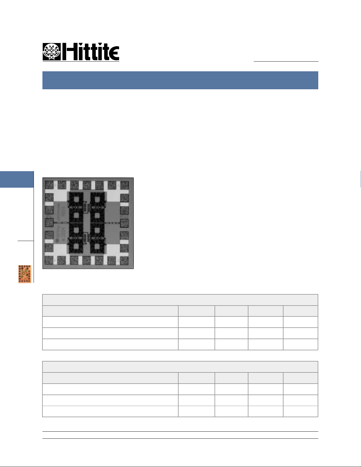
The HMC158 is a miniature frequency doubler in a MMIC die. Suppression of undesired fundamental and higher order harmonics is 34 to 58 dB with respect to input signal
level and 19 to 45 dB with respect to the
desired output signal level. The doubler
uses the same diode/balun technology used
in Hittite MMIC mixers, features small size
and requires no DC bias.
Guaranteed Perf ormance, 50 Ohm system -55 to +85 deg C
Typical Performance vs.Drive Level
10 15 20 dBm
Input Frequency Range 1.7-4.0 1.7-3.5 1.3-4.0 GHz
Output Frequency Range 3.4-8.0 3.4-7.0 2.6-8.0 GHz
Conversion Loss <20 <15 <15 d B
Performance for Input Signals in the 1.7 - 3.5 GHz Band (+15dBm Drive)
Min. Typ. Max.
Fo Isolation (with respect to i nput level ) 37 45 dB
3Fo Isolation (with respect to i np ut level) 40 50 dB
4Fo Isolation (with respect to input level) 32 40 dB
12 Elizabeth Drive, Chelmsford, MA 01824 Phone: 978-250-3343 Fax: 978-250-3373 Web Site: www.hittite.com
3 - 18
Page 2
MICROWAVE CORPORATION
-100
-90
-80
-70
-60
-50
-40
-30
-20
-10
0
0 5 10 15 20
3Fo
4Fo
Fo
ISOLATION (dB)
FREQUENCY (GHz)
HMC158 SMT FREQUENCY DOUBLER 1.3 - 4.0 GHz INPUT
HMC158
FEBRUARY 2001
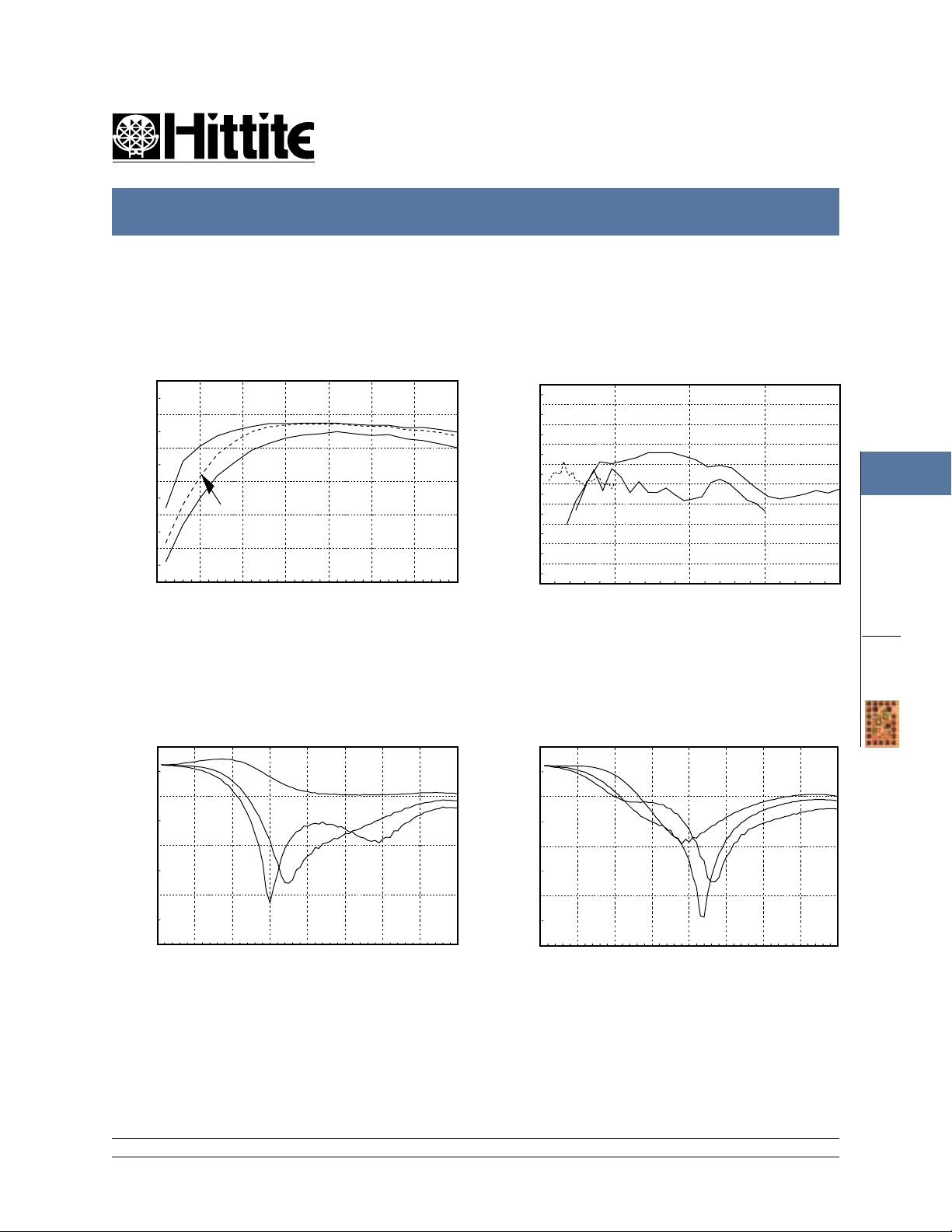
Conversion Loss vs. Drive Level
0
-10
Input=+20dBm
-20
-30
-40
CONVERSION LOSS (dB)
-50
Input=+10dBm
-60
12345678
Input=+15dBm
OUTPUT FREQUENCY (GHz)
Input Return Loss vs. Drive level
0
-10
Input=+10dBm
Isolation @ +15 dBm Drive Level *
* With respect to input level
Output Return Loss vs. Drive Level
0
-10
Input=+10dBm
3
MULTIPLIERS
DIE
-20
-30
INPUT RETURN LOSS (dB)
-40
012345678
12 Elizabeth Drive, Chelmsford, MA 01824 Phone: 978-250-3343 Fax: 978-250-3373 Web Site: www.hittite.com
Input =+20dBm
INPUT FREQUENCY (GHz)
Input =+15dBm
-20
-30
Input=+15dBm
-40
OUTPUT RETURN LOSS (dB)
012345678
OUTPUT FREQUENCY (GHz)
Input=+20dBm
3 - 19
Page 3

MICROWAVE CORPORATION
HMC158 SMT FREQUENCY DOUBLER 1.3 - 4.0 GHz INPUT
FEBRUARY 2001
HMC158
3
MULTIPLIERS
DIE
Schematic
Outline Drawing
1.168
(0.046)
0.127
(0.005)
0.584
(0.023)
Absolute Maximum Ratings
Input Drive +27 dBm
Storage Temperature -65 to +150 deg C
Operating Temperature -55 to +125 deg C
1.168
(0.046)
1.041
(0.041)
4614
RFin RFout
Hittite
RF OUTRF IN
0.584
(0.023)
THREE PADS ON EACH CORNER MUST BE BONDED TO GROUND (12 TOTAL).
ALL DIMENSIONS IN MILLIMETERS (INCHES)
ALL TOLERANCES ARE ±0.025 (0.001)
DIE THICKNESS IS 0.254 (0.010)
BONDPADS ARE 0.100 (0.004) SQUARE
EQUALLY SPACED AT 0.150 (0.006) CENTERS
BACKSIDE METALLIZATION: NONE
BOND PAD METALLIZATION : GOLD
12 Elizabeth Drive, Chelmsford, MA 01824 Phone: 978-250-3343 Fax: 978-250-3373 Web Site: www.hittite.com
3 - 20
Page 4

HMC158
MICROWAVE CORPORATION
HMC158 SMT FREQUENCY DOUBLER 1.3 - 4.0 GHz INPUT
FEBRUARY 2001
Handling Precautions
Follow these precautions to avoid permanent damage.
Cleanliness: Handle the chips in a clean environment. DO NOT attempt to clean the chip using liquid
cleaning systems.
Static Sensitivity: Follow ESD precautions to protect against > ± 250V ESD strikes ( see page 8 - 2 ).
Transients: Suppress instrument and bias supply transients while bias is applied. Use shielded signal and
bias cables to minimize inductive pick-up.
General Handling: Handle the chip along the edges with a vacuum collet or with a sharp pair of bent tweezers. The surface of the chip has fragile air bridges and should not be touched with vacuum collet, tweezers, or fingers.
Mounting
3
The chip is not back-metallized and can be die mounted with electrically conductive epoxy. The mounting
surface should be clean and flat.
Epoxy Die Attach:
Apply a minimum amount of epoxy to the mounting surface so that a thin epoxy fillet is observed around
the perimeter of the chip once it is placed into position.
Cure epoxy per the manufacturer's schedule.
Wire Bonding
Ball or wedge bond with 1.0 diameter pure gold wire. Thermosonic wirebonding with a nominal stage
temperature of 150 deg. C and a ball bonding force of 40 to 50 grams or wedge bonding force of 18 to 22
grams is recommended. Use the minimum level of ultrasonic energy to achieve reliable wirebonds.
Wirebonds should be started on the chip and terminated on the package. RF bonds should be as short as
possible.
MULTIPLIERS
DIE
12 Elizabeth Drive, Chelmsford, MA 01824 Phone: 978-250-3343 Fax: 978-250-3373 Web Site: www.hittite.com
3 - 21
 Loading...