

Page 1

HM62G36256 Series
8M Synchronous Fast Static RAM
(256k-word × 36-bit)
ADE-203-1139 (Z)
Preliminary
Rev. 0.0
Jan. 10, 2000
Description
The HM62G36256 is a synchronous fast static RAM organized as 256-kword × 36-bit. It has realized high
speed access time by employing the most advanced CMOS process and high speed circuit designing
technology. It is most appropriate for the application which requires high speed, high density memory and
wide bit width configuration, such as cache and buffer memory in system. It is packaged in standard 119bump BGA.
Note: All power supply and ground pins must be connected for proper operation of the device.
Features
• Power supply: 3.3 V +10%, –5%
• Clock frequency: 200 MHz to 250 MHz
• Internal self-timed late write
• Byte write control (4 byte write selects, one for each 9-bit)
• Optional ×18 configuration
• HSTL compatible I/O
• Programmable impedance output drivers
• User selective input trip-point
• Differential, HSTL clock inputs
• Asynchronous G output control
• Asynchronous sleep mode
• Limited set of boundary scan JTAG IEEE 1149.1 compatible
• Protocol: Single clock register-register mode
Preliminary: The specifications of this device are subject to change without notice. Please contact your
nearest Hitachi’s Sales Dept. regarding specifications.
Page 2
HM62G36256 Series
Ordering Information
Type No. Access time Cycle time Package
HM62G36256BP-4
HM62G36256BP-5
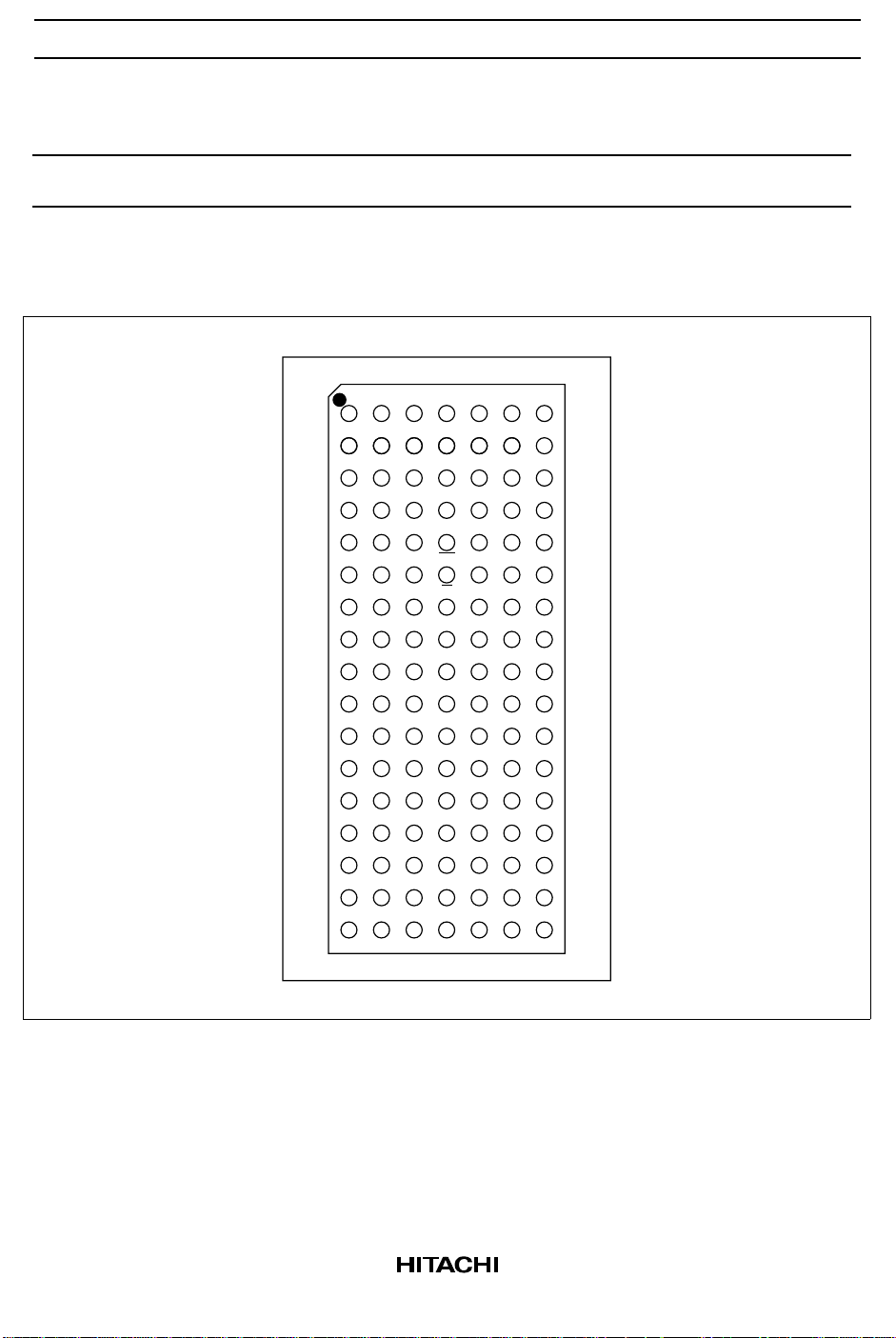
Pin Arrangement
2.1 ns
2.5 ns
4.0 ns
5.0 ns
119-bumps BGA
1234567
A
VDDQ SA0 SA6 NC SA4 SA2 VDDQ
B
NC NC SA7 NC SA8 SA9 NC
C
NC SA14 SA3 VDD SA5 SA1 NC
D
DQc1 DQc0 VSS ZQ VSS DQb0 DQb1
E
DQc2 DQc3 VSS SS VSS DQb3 DQb2
F
VDDQ DQc4 VSS G VSS DQb4 VDDQ
G
DQc6 DQc5 SWEc NC DQb5 DQb6
H
DQc7 DQc8 VSS NC VSS DQb8 DQb7
J
VDDQ VDD VREF VDD VREF VDD VDDQ
K
DQd7 DQd8 VSS K VSS DQa8 DQa7
L
DQd6 DQd5 K SWEa DQa5 DQa6
M
VDDQ DQd4 VSS SWE VSS DQa4 VDDQ
N
DQd2 DQd3 VSS SA17 VSS DQa3 DQa2
P
DQd1 DQd0 VSS SA16 VSS DQa0 DQa1
R
NC SA10 M1 VDD M2 SA11 NC
T
NC NC SA12 SA15 SA13 NC ZZ
U
VDDQ TMS TDI TCK TDO NC VDDQ
SWEd
SWEb
119-bump 1. 27 mm
14 mm × 22 mm BGA (BP-119A)
(Top view)
2
Page 3

HM62G36256 Series
Pin Description
Name I/O type Descriptions Notes
V
DD
V
SS
V
DDQ
V
REF
K Input Clock input. Active high.
K Input Clock input. Active low.
SS Input Synchronous chip select
SWE Input Synchronous write enable
SAn Input Synchronous address input n = 0, 1, 2...17
SWEx Input Synchronous byte write enables x = a, b, c, d
G Input Asynchronous output enable
ZZ Input Power down mode select
ZQ Input Output impedance control 1
DQxn I/O Synchronous data input/output x = a, b, c, d
M1, M2 Input Output protocol mode select
TMS Input Boundary scan test mode select
TCK Input Boundary scan test clock
TDI Input Boundary scan test data input
TDO Output Boundary scan test data output
NC — No connection
Supply Core power supply
Supply Ground
Supply Output power supply
Supply Input reference: provides input reference voltage
n = 0, 1, 2...8
M1 M2 Protocol Notes
V
SS
V
DD
Synchronous register to register operation 2
Notes: 1. ZQ is to be connected to VSS via a resistance RQ where 150 Ω ≤ RQ ≤ 300 Ω, if ZQ = V
open, output buffer impedance will be maximum. A case of minimum impedance, it needs to
connect over 120 Ω between ZQ and V
2. There is 1 protocol with mode pin. Mode control pins (M1, M2) are to be tied either V
.
SS
DD
respectively. The state of the Mode control inputs must be set before power-up and must not
change during device operation. Mode control inputs are not standard inputs and may not meet
V
or VIL specification. This SRAM is tested only in the synchronous register to register
IH
operation.
DDQ
or V
or
SS
3
Page 4
HM62G36256 Series
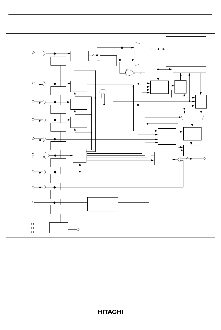
Block Diagram
A0 to A17
SS
SWE
SWEx
ZZ
V
REF
ZQ
18
JTAG
register
JTAG
register
JTAG
register
4
JTAG
register
G
K
K
JTAG
register
JTAG
register
JTAG
register
JTAG
register
JTAG
register
R-Add
register
SS
register
SWE
register
SWEx
register
CLK
control
18
W-Add
register
4
Impedance
contorol logic
18
MUX
1
WRC
Match
DOC
D-in
register
Memory
cell array
(256k × 36)
Row decoder
Column decoder
WA
Multiplex
D-out
register
OB
36
SA
DQa0-8
DQb0-8
DQc0-8
DQd0-8
TDI
TCK
TMS
JTAG tap
controller
TDO
4
Page 5

HM62G36256 Series
Operation Table
ZZ SS G SWE SWEa SWEb SWEc SWEd K K Operation DQ (n) DQ (n + 1)
H ××ЧЧЧЧЧЧ×sleep mode High-Z High-Z
LH×ЧЧЧЧЧL-H H-L Dead
(not selected)
L × H ЧЧЧЧЧЧ×Dead
(Dummy read)
LLLH ××××L-H H-L Read × Dout
LL× LLLLLL-HH-LWrite a, b, c, d
byte
LL× L H L L L L-H H-L Write b, c, d
byte
LL× L L H L L L-H H-L Write a, c, d
byte
LL× LLLHLL-HH-LWrite a, b, d
byte
LL× LLLLHL-HH-LWrite a, b, c
byte
LL× L H H L L L-H H-L Write c, d byte High-Z Din (c,d)0-8
LL× L L H H L L-H H-L Write a, d byte High-Z Din (a,d)0-8
LL× L L L H H L-H H-L Write a, b byte High-Z Din (a,b)0-8
LL× L H L L H L-H H-L Write b, c byte High-Z Din (b,c)0-8
LL× LHHHLL-HH-LWrite d byte High-Z Din (d)0-8
LL× L H H L H L-H H-L Write c byte High-Z Din (c)0-8
LL× L H L H H L-H H-L Write b byte High-Z Din (b)0-8
LL× L L H H H L-H H-L Write a byte High-Z Din (a)0-8
Notes: 1. × means don’t care for synchronous inputs, and H or L for asynchronous inputs.
2. SWE , SS, SWEa to SWEd, SA are sampled at the rising edge of K clock.
3. Although differential clock operation is implied, this SRAM will operate properly with one clock
phase (either K or K) tied to V
specified within this document will be met.
. Under such single-ended clock operation, all parameters
REF
× High-Z
High-Z High-Z
(a,b,c,d)0-8
High-Z Din (a,b,c,d)0-8
High-Z Din (b,c,d)0-8
High-Z Din (a,c,d)0-8
High-Z Din (a,b,d)0-8
High-Z Din (a,b,c)0-8
5
Page 6
HM62G36256 Series
Absolute Maximum Ratings
Parameter Symbol Value Unit Notes
Input voltage on any pin V
Core supply voltage V
Output supply voltage V
Operating temperature T
Storage temperature T
IN
DD
DDQ
OPR
STG
–0.5 to V
–0.5 to 3.9 V 1
–0.5 to 2.2 V 1, 4
0 to 70 °C
–55 to 125 °C
Junction temperature Tj 110 °C
Output short–circuit current I
Latch up current I
OUT
LI
25 mA
200 mA
Package junction to case thermal resistance θJC 5 °C/W 5, 7
Package junction to ball thermal resistance θJB 8 °C/W 6, 7
Notes: 1. All voltage is referred to VSS.
2. Permanent device damage may occur if Absolute Maximum Ratings are exceeded. Functional
operation should be restricted the Operation Conditions. Exposure to higher than recommended
voltages for extended periods of time could affect device reliability.
3. These CMOS memory circuits have been designed to meet the DC and AC specifications shown
in the tables after thermal equilibrium has been established.
4. The supply voltage application sequence need to be powered up in the following manner: V
V
, V
, V
DD
DDQ
then VIN. Remember, according to the Absolute Maximum Ratings table, V
REF
not to exceed 3.9 V, whatever the instantaneous value of V
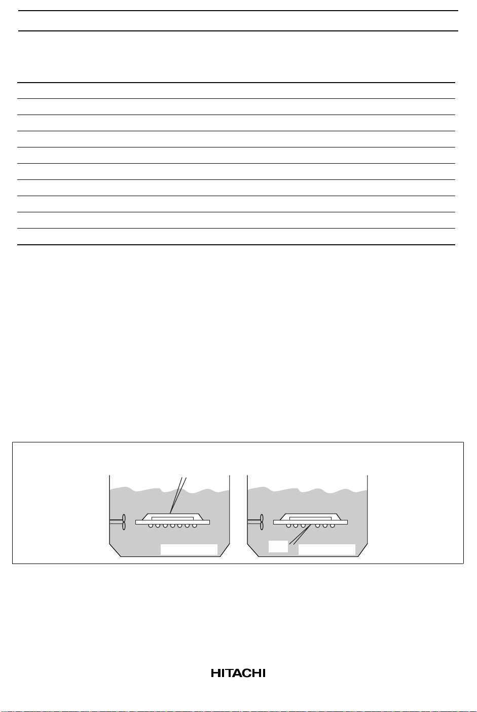
5. θJC is measured at the center of mold surface in fluorocarbon (See Figure “Definition of
Measurement”).
6. θJB is measured on the center ball pad after removing the ball in fluorocarbon (See Figure
“Definition of Measurement”).
7. These thermal resistance values have error of ± 5°C/W.
+ 0.5 V 1, 4
DDQ
.
DDQ
DDQ
,
SS
is
θJC
θJB
T.C.
Fluorocarbon
T.C.
Fluorocarbon
Definition of Measurement
6
Page 7
HM62G36256 Series
Note: The following the DC and AC specifications shown in the Tables, this device is tested under the
minimum transverse air flow exceeding 500 linear feet per minute.
DC Operating Conditions (Ta = 0 to 70°C [Tj max = 110°C])
Parameter Symbol Min Typ Max Unit Notes
Supply voltage (Core) V
Supply voltage (I/O) V
Supply voltage V
Input reference voltage (I/O) V
Input high voltage V
Input low voltage V
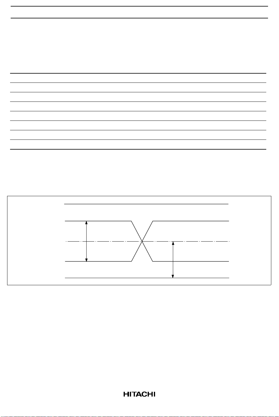
Clock differential voltage V
Clock common mode voltage V
DD
DDQ
SS
REF
IH
IL
DIF
CM
Notes: 1. Peak to peak AC component superimposed on V
2. Minimum differential input voltage required for differential input clock operation.
3. See following figure.
4. V
= 0.75 V (typ).
REF
3.135 3.30 3.63 V
1.4 1.5 1.6 V
000 V
0.65 0.75 0.90 V 1
V
+ 0.1 — V
REF
–0.5 — V
0.1 — V
+ 0.3 V 4
DDQ
– 0.1 V 4
REF
+ 0.3 V 2, 3
DDQ
0.55 — 0.90 V 3
may not exceed 5% of V
REF
REF
.
V
DDQ
V
SS
V
DIF
V
CM
Differential Voltage/Common Mode Voltage
7
Page 8
HM62G36256 Series
DC Characteristics (Ta = 0 to 70°C, [Tj max = 110°C], VDD = 3.3 V +10%, –5%)
Parameter Symbol Min Typ Max Unit Notes
Input leakage current I
Output leakage current I
Standby current I
VDD operating current,
excluding output drivers
4 ns cycle
VDD operating current,
excluding output drivers
5 ns cycle
Quiescent active power
supply current
Output low voltage V
Output high voltage V
ZQ pin connect
resistance
Output low current I
Output high current I
Notes: 1. 0 ≤ Vin ≤ V
2. 0 ≤ Vout ≤ V
DDQ
DDQ
3. All inputs (except clock) are held at either V
guaranteed at 75°C junction temperature.
4. Iout = 0 mA, read 50%/write 50%, V
5
. Iout = 0 mA, read 50%/write 50%, V
6. Minimum impedance push pull output buffer mode, I
7. Measured at V
8. Measured at V
9. Output buffer impedance can be programmed by terminating the ZQ pin to V
precision resister (RQ). The value of RQ is five times the output impedance desired. The
allowable range of RQ to guarantee impedance matching with a tolerance of 15% is between
150 Ω and 300 Ω. If the status of ZQ pin is open, output impedance is maximum. Maximum
impedance occurs with ZQ connected to V
occurs when the SRAM is in High-Z. Write and Deselect operations will synchronously switch
the SRAM into and out of High-Z, therefore triggering an update. The user may choose to
invoke asynchronous G updates by providing a G setup and hold about the K clock to guarantee
the proper update. At power-up, the output impedance defaults to minimum impedance. It will
take 2048 cycles for the impedance to be completely updated if the programmed impedance is
much higher than minimum impedance.
LI
LO
SBZZ
I
DD4
I
DD5
I
DD2
RQ 150 250 300 Ω
OL
OH
for all input pins (except V
OL
OH
——2 µA1
——5 µA2
— — 100 mA 3
— — 700 mA 4
— — 650 mA 4
— — 200 mA 5
V
OL
OH
SS
V
– 0.4 — V
DDQ
(V
/2)/[(RQ/5)–15%] — (V
DDQ
(V
/2)/[(RQ/5–4)+15%] — (V
DDQ
REF
—VSS + 0.4 V 6
DDQ
/2)/[(RQ/5)+15%] mA 7, 9
DDQ
/2)/[(RQ/5–4)–15%] mA 8, 9
DDQ
, ZQ, M1, M2 pin).
, DQ in High-Z.
or VIL, ZZ is held at VIH, Iout = 0 mA, Spec is
IH
= VDD max, VIN = VIH or VIL, Frequency = minimum cycle.
DD
= VDD max, VIN = VIH or VIL, Frequency = 3 MHz.
DD
= –6 mA, IOL = 6 mA.
OH
= 1/2 V
= 1/2 V
DDQ
DDQ
.
.
. The impedance update of the output driver
DDQ
through a
SS
V6
8
Page 9

HM62G36256 Series
Capacitance (Ta = 25°C, f = 1 MHz)
Parameter Symbol Min Max Unit Note
Input capacitance (SAn, SS, SWE, SWEx)C
Input capacitance (K, K, G)C
Input/Output capacitance (DQxn) C
Note: 1. This parameter is sampled and not 100% tested.
IN
CLK
IO
AC Characteristics (Ta = 0 to 70°C, [Tj max = 110°C], VDD = 3.3 V +10%, –5%)
Test Conditions
— 4 pF 1
— 7 pF 1
— 5 pF 1
• Input pulse levels (K, K): V
= 0.75 V, VCM = 0.75 V
DIF
• Input timing reference level (K, K): Differential cross point
• Input pulse levels (except K, K): VIL = 0.25 V, VIH = 1.25 V
• Input and output timing reference levels (except K, K): V
= 0.75 V
REF
• Input rise and fall time: 0.5 ns (10% to 90%)
• Measurement condition: the minimum impedance push pull output buffer mode, IOH = –6 mA, IOL = 6
mA
• Output driver supply voltage: V
DDQ
= 1.5 V
• Output load: See figure
50 Ω
0.75 V
50 Ω
0.75 V
DQ
16.7 Ω
16.7 Ω
16.7 Ω 50 Ω
50 Ω
5 pF
5 pF
0.75 V
9
Page 10

HM62G36256 Series
Single Differential Clock Register-Register Mode (M1 = VSS, M2 = VDD)
HM62G36256
-4 -5
Parameter Symbol Min Max Min Max Unit Notes
CK clock cycle time t
CK clock high width t
CK clock low width t
Address setup time t
Data setup time t
Address hold time t
Data hold time t
Clock high to output valid t
Clock high to output hold t
Clock high to output valid
(SS control)
Clock high to output High-Z t
Output enable low to output Low-Z t
Output enable low to output valid t
Output enable low to output High-Z t
Sleep mode recovery time t
Sleep mode enable time t
Notes: 1. Guaranteed by design.
2. Refer to the Test Conditions.
3. Transitions are measured at start point of output high impedance from output low impedance.
4. Output driver impedance updates during High-Z.
5. Transitions are measured ±50 mV from steady state voltage.
6. When ZZ is switching, clock input K must be at same logic levels for reliable operation.
KHKH
KHKL
KLKH
AVKH
DVKH
KHAX
KHDX
KHQV
KHQX
t
KHQX2
KHQZ
GLQX
GLQV
GHQZ
ZZR
ZZE
4.0 — 5.0 — ns
1.5 — 1.5 — ns
1.5 — 1.5 — ns
0.5 — 0.5 — ns
0.5 — 0.5 — ns
0.75 — 1.0 — ns 1
0.75 — 1.0 — ns 1
— 2.1 — 2.5 ns 2
0.5 — 0.5 — ns 2
— 2.1 — 2.5 ns 2, 5
— 2.5 — 3.0 ns 2, 3
0.5 — 0.5 — ns 2, 5
— 2.5 — 2.5 ns 2, 3
— 2.5 — 2.5 ns 2, 3
10.0 — 10.0 — ns 6
— 10.0 — 10.0 ns 2, 3, 6
10
Page 11

Timing Waveforms
Read Cycle-1
HM62G36256 Series
K
K
SA
A1 A2 A3 A4
SS
SWE
SWEx
DQ
Note: G, ZZ = V
t
KHKH
t
AVKH
t
AVKH
t
AVKH
t
KHKLtKLKH
t
KHAX
t
KHAX
t
KHAX
t
KHQX
Do 1Do 0 Do 2
t
KHQV
IL
11
Page 12

HM62G36256 Series
Read Cycle-2 (SS Controlled)
K
K
SA
A1 A3 A4
SS
SWE
SWEx
DQ
Note: G, ZZ = V
t
AVKH
t
KHAX
t
AVKH
t
KLKH
t
KHQZ
t
KHAX
t
KHAX
t
KHKH
t
AVKH
t
KHKL
Do 0 Do 1 Do 3
t
KHQX2
IL
12
Page 13

Read Cycle-3 (G Controlled)
HM62G36256 Series
t
KHKH
t
KHKL
t
KLKH
K
K
SA
t
AVKH
A1 A2 A3 A4
t
AVKH
t
KHAX
t
KHAX
SS
t
AVKH
t
KHAX
SWE
SWEx
G
t
GHQZ t
GLQV
DQ Do 1Do 0 Do 3
t
Note: ZZ = V
IL
GLQX
13
Page 14

HM62G36256 Series
Write Cycle
K
K
SA
SS
SWE
SWEx
G
DQ
Note: ZZ = V
t
KHAX
t
KLKH
t
KHKH
t
AVKH
t
KHKL
A1 A2 A3 A4
t
AVKH
t
AVKH
t
AVKH
t
DVKH
t
KHAX
t
KHAX
t
KHAX
t
KHDX
Di 0 Di 1 Di 2 Di 3
IL
14
Page 15

Read-Write Cycle
HM62G36256 Series
SA
SS
SWE
SWEx
G
DQ
Note: ZZ = V
ZZ Control
READ WRITEREAD
(G control)
t
KHKH
t
KHKL
t
KLKH
READ DEAD
(SS control)
WRITE
K
K
t
AVKH
t
KHAX
A7A6A4A3A1
t
AVKH
t
KHAX
t
AVKH
t
AVKH
t
GHQZ
t
KHAX
t
KHAX
t
DVKHtKHDX
t
GLQV
Do 0 Do 1 Do 4Di 3 Di 6
t
KHQX
t
KHQV
t
GLQX
t
KHQZ
IL
K
K
SA
SS
SWE
SWEx
ZZ
Sleep active
DQ
Note: G = V
t
KHKH
t
AVKH
t
AVKH
IL
t
ZZR
A1
t
KHKL
t
KHAX
t
KHAX
t
KLKH
Sleep off
Do 1
Sleep active
t
ZZE
15
Page 16

HM62G36256 Series
Boundary Scan Test Access Port Operations
In order to perform the interconnect testing of the modules that include this SRAM, the serial boundary
scan test access port (TAP) is designed to operate in a manner consistent with IEEE Standard 1149.1 -
1990. But does not implement all of the functions required for 1149.1 compliance The HM62Gxx series
contains a TAP controller. Instruction register, Boundary scans register, Bypass register and ID register.
Test Access Port Pins
Symbol I/O Name
TCK Test clock
TMS Test mode select
TDI Test data in
TDO Test data out
Note: This Device does not have a TRST (TAP Reset) pin. TRST is optional in IEEE 1149.1.
To disable the TAP, TCK must be connected to V
To test Boundary scan, ZZ pin need to be kept below V
TAP DC Operating Conditions (Ta = 0 to 70°C, [Tj max = 110°C])
. TDO should be left unconnected.
SS
– 0.4 V.
REF
Parameter Symbol Min Max Unit Notes
Boundary scan input high voltage V
Boundary scan input low voltage V
Boundary scan input leakage current I
Boundary scan output low voltage V
Boundary scan output high voltage V
IH
IL
LI
OL
OH
2.0 VDD + 0.3 V
–0.5 0.8 V
–2 2 µA1
— 0.4 V 2
2.4 — V 3
Notes: 1. 0 ≤ Vin ≤ VDD for all logic input pin.
2. I
= 8 mA.
OL
3. I
= –8 mA.
OH
16
Page 17

HM62G36256 Series
TAP AC Characteristics (Ta = 0 to 70°C, [Tj max = 110°C])
Parameter Symbol Min Max Unit Note
Test clock cycle time t
Test clock high pulse width t
Test clock low pulse width t
Test mode select setup t
Test mode select hold t
Capture setup t
Capture hold t
TDI valid to TCK high t
TCK high to TDI don’t care t
TCK low to TDO unknown t
TCK low to TDO valid t
THTH
THTL
TLTH
MVTH
THMX
CS
CH
DVTH
THDX
TLQX
TLQV
Note: 1. tCS + tCH defines the minimum pause in RAM I/O pad transitions to assure pad data capture.
TAP Test Conditions
67 — ns
30 — ns
30 — ns
10 — ns
10 — ns
10 — ns 1
10 — ns 1
10 — ns
10 — ns
0—ns
—20ns
• Input pulse levels: 0 to 3.0 V
• Input and output timing reference levels: 1.5 V
• Input rise and fall time: 2 ns (10% to 90%) (typ)
• Output Load: See figure
DUT
Z
0
TDO
VT = 1.5 V
50 Ω
= 50 Ω
17
Page 18

HM62G36256 Series
TAP Controller Timing Diagram
t
THTHtTHTLtTLTH
TCK
t
MVTH
t
THMX
TMS
t
DVTH
t
THDX
TDI
t
TLQV
t
TLQX
TDO
RAM
t
CS
t
CH
Address
Test Access Port Registers
Register name Length Symbol Note
Instruction register 3 bits IR [0;2]
Bypass register 1 bit BP
ID register 32 bits ID [0;31]
Boundary scan register 70 bits BS [1;70]
18
Page 19

HM62G36256 Series
TAP Controller Instruction Set
IR2 IR1 IR0 Instruction Operation
0 0 0 SAMPLE-Z Tristate all data drivers and capture the pad value
0 0 1 IDCODE
0 1 0 SAMPLE-Z Tristate all data drivers and capture the pad value
0 1 1 BYPASS
1 0 0 SAMPLE
1 0 1 BYPASS
1 1 0 BYPASS
1 1 1 BYPASS
Note: This Device does not perform EXTEST, INTEST or the preload portion of the PRELOAD command
in IEEE 1149.1.
19
Page 20

HM62G36256 Series
Boundary Scan Order
Bit No. Bump ID Signal name Bit No. Bump ID Signal name
1 5R M2 36 3B SA7
2 4P SA16 37 2B NC
3 4T SA15 38 3A SA6
4 6R SA11 39 3C SA3
5 5T SA13 40 2C SA14
6 7T ZZ 41 2A SA0
7 6P DQa0 42 2D DQc0
8 7P DQa1 43 1D DQc1
9 6N DQa3 44 2E DQc3
10 7N DQa2 45 1E DQc2
11 6M DQa4 46 2F DQc4
12 6L DQa5 47 2G DQc5
13 7L DQa6 48 1G DQc6
14 6K DQa8 49 2H DQc8
15 7K DQa7 50 1H DQc7
16 5L SWEa 51 3G SWEc
17 4L K 52 4D ZQ
18 4K K 53 4E SS
19 4F G 54 4G NC
20 5G SWEb 55 4H NC
21 7H DQb7 56 4M SWE
22 6H DQb8 57 3L SWEd
23 7G DQb6 58 1K DQd7
24 6G DQb5 59 2K DQd8
25 6F DQb4 60 1L DQd6
26 7E DQb2 61 2L DQd5
27 6E DQb3 62 2M DQd4
28 7D DQb1 63 1N DQd2
29 6D DQb0 64 2N DQd3
30 6A SA2 65 1P DQd1
31 6C SA1 66 2P DQd0
32 5C SA5 67 3T SA12
33 5A SA4 68 2R SA10
34 6B SA9 69 4N SA17
35 5B SA8 70 3R M1
20
Page 21

Notes: 1. Bit number1 is the first scan bit to exit the chip.
2. The NC pads listed in this table are indeed no connects, but are represented in the boundary
scan register by a “Place Holder”. Placeholder registers are internally connected to V
3. In Boundary scan mode, differential input K and K are referred to each other and must be at
opposite logic levels for reliable operation.
4. ZZ must remain at V
during boundary scan.
IL
5. In boundary scan mode, ZQ must be driven to V
6. M1 and M2 must be driven to V
or VSS supply rail to ensure consistent results.
DD
HM62G36256 Series
.
SS
or VSS supply rail to ensure consistent results.
DDQ
21
Page 22

HM62G36256 Series
ID register
Bit No.
31×30×29×28×2702602512412302202102011901801701601501401301201101009080706050403121110
Value
1
Vendor
Revision No.
Depth Width Use in the future Vendor ID No. Fix
TAP Controller State Diagram
1
0
Test-Logic-
Reset
0
Run-Test/
Idle
Select-
DR-Scan
Capture-DR
Shift-DR
Exit1-DR
Pause-DR
Exit2-DR
11
0
0
0
1
1
00
00
1
1
IR-Scan
11
Capture-IR
Shift-IR
Exit1-IR
Pause-IR
00
Exit2-IR
Select-
1
0
0
0
1
1
1
1
22
Update-DR
1
Note: The value adjacent to each state transition in this figure represents the signal present
at TMS at the time of a rising edge at TCK.
No matter what the original state of the controller, it will enter Test-Logic-Reset when
TMS is held high for at least five rising edges of TCK.
00
Update-IR
1
Page 23

Package Dimensions
HM62G36256BP Series (BP-119A)
HM62G36256 Series
Unit: mm
0.204 ×
4 × C1.2
Pin 1 Index
22.00
B
φ
119 × 0.75 ± 0.15
φ
0.30
φ
0.15 C
0.60 ± 0.10
M
M
14.00
13.0 ± 0.10
CAB
A
2.10 ± 0.25
C
0.35 C
0.15 C
21.0 ± 0.10
1.27
1.27
Y
1234567
A
B
C
D
E
F
G
H
J
K
L
M
N
P
R
T
U
Details of the part Y
Hitachi Code
JEDEC
EIAJ
(reference value)
Weight
BP-119A
Conforms
—
1.2 g
23
Page 24

HM62G36256 Series
Cautions
1. Hitachi neither warrants nor grants licenses of any rights of Hitachi’s or any third party’s patent,
copyright, trademark, or other intellectual property rights for information contained in this document.
Hitachi bears no responsibility for problems that may arise with third party’s rights, including
intellectual property rights, in connection with use of the information contained in this document.
2. Products and product specifications may be subject to change without notice. Confirm that you have
received the latest product standards or specifications before final design, purchase or use.
3. Hitachi makes every attempt to ensure that its products are of high quality and reliability. However,
contact Hitachi’s sales office before using the product in an application that demands especially high
quality and reliability or where its failure or malfunction may directly threaten human life or cause risk
of bodily injury, such as aerospace, aeronautics, nuclear power, combustion control, transportation,
traffic, safety equipment or medical equipment for life support.
4. Design your application so that the product is used within the ranges guaranteed by Hitachi particularly
for maximum rating, operating supply voltage range, heat radiation characteristics, installation
conditions and other characteristics. Hitachi bears no responsibility for failure or damage when used
beyond the guaranteed ranges. Even within the guaranteed ranges, consider normally foreseeable
failure rates or failure modes in semiconductor devices and employ systemic measures such as failsafes, so that the equipment incorporating Hitachi product does not cause bodily injury, fire or other
consequential damage due to operation of the Hitachi product.
5. This product is not designed to be radiation resistant.
6. No one is permitted to reproduce or duplicate, in any form, the whole or part of this document without
written approval from Hitachi.
7. Contact Hitachi’s sales office for any questions regarding this document or Hitachi semiconductor
products.
Hitachi, Ltd.
Semiconductor & Integrated Circuits.
Nippon Bldg., 2-6-2, Ohte-machi, Chiyoda-ku, Tokyo 100-0004, Japan
Tel: Tokyo (03) 3270-2111 Fax: (03) 3270-5109
URL NorthAmerica : http:semiconductor.hitachi.com/
For further information write to:
Hitachi Semiconductor
(America) Inc.
179 East Tasman Drive,
San Jose,CA 95134
Tel: <1> (408) 433-1990
Fax: <1>(408) 433-0223
Europe : http://www.hitachi-eu.com/hel/ecg
Asia (Singapore) : http://www.has.hitachi.com.sg/grp3/sicd/index.htm
Asia (Taiwan) : http://www.hitachi.com.tw/E/Product/SICD_Frame.htm
Asia (HongKong) : http://www.hitachi.com.hk/eng/bo/grp3/index.htm
Japan : http://www.hitachi.co.jp/Sicd/index.htm
Hitachi Europe GmbH
Electronic components Group
Dornacher Straße 3
D-85622 Feldkirchen, Munich
Germany
Tel: <49> (89) 9 9180-0
Fax: <49> (89) 9 29 30 00
Hitachi Europe Ltd.
Electronic Components Group.
Whitebrook Park
Lower Cookham Road
Maidenhead
Berkshire SL6 8YA, United Kingdom
Tel: <44> (1628) 585000
Fax: <44> (1628) 778322
Hitachi Asia Pte. Ltd.
16 Collyer Quay #20-00
Hitachi Tower
Singapore 049318
Tel: 535-2100
Fax: 535-1533
Hitachi Asia Ltd.
Taipei Branch Office
3F, Hung Kuo Building. No.167,
Tun-Hwa North Road, Taipei (105)
Tel: <886> (2) 2718-3666
Fax: <886> (2) 2718-8180
Copyright © Hitachi, Ltd., 1998. All rights reserved. Printed in Japan.
24
Hitachi Asia (Hong Kong) Ltd.
Group III (Electronic Components)
7/F., North Tower, World Finance Centre,
Harbour City, Canton Road, Tsim Sha Tsui,
Kowloon, Hong Kong
Tel: <852> (2) 735 9218
Fax: <852> (2) 730 0281
Telex: 40815 HITEC HX
 Loading...