

Datasheet HM6264BLFP-10LT, HM6264BLFP-8LT, HM6264BLP-10L, HM6264BLP-8L, HM6264BLSP-10L Datasheet (HIT)
...Page 1

HM6264B Series
64 k SRAM (8-kword × 8-bit)
ADE-203-454B (Z)
Rev. 2.0
Nov. 1997
Description
The Hitachi HM6264B is 64k-bit static RAM organized 8-kword × 8-bit. It realizes higher performance
and low power consumption by 1.5 µm CMOS process technology. The device, packaged in 450 mil
SOP (foot print pitch width), 600 mil plastic DIP, 300 mil plastic DIP, is available for high density
mounting.
Features
• High speed
Fast access time: 85/100 ns (max)
• Low power
Standby: 10 µW (typ)
Operation: 15 mW (typ) (f = 1 MHz)
• Single 5 V supply
• Completely static memory
No clock or timing strobe required
• Equal access and cycle times
• Common data input and output
Three state output
• Directly TTL compatible
All inputs and outputs
• Battery backup operation capability
Page 2
HM6264B Series
Ordering Information
Type No. Access time Package
HM6264BLP-8L
HM6264BLP-10L
HM6264BLSP-8L
HM6264BLSP-10L
HM6264BLFP-8LT
HM6264BLFP-10LT
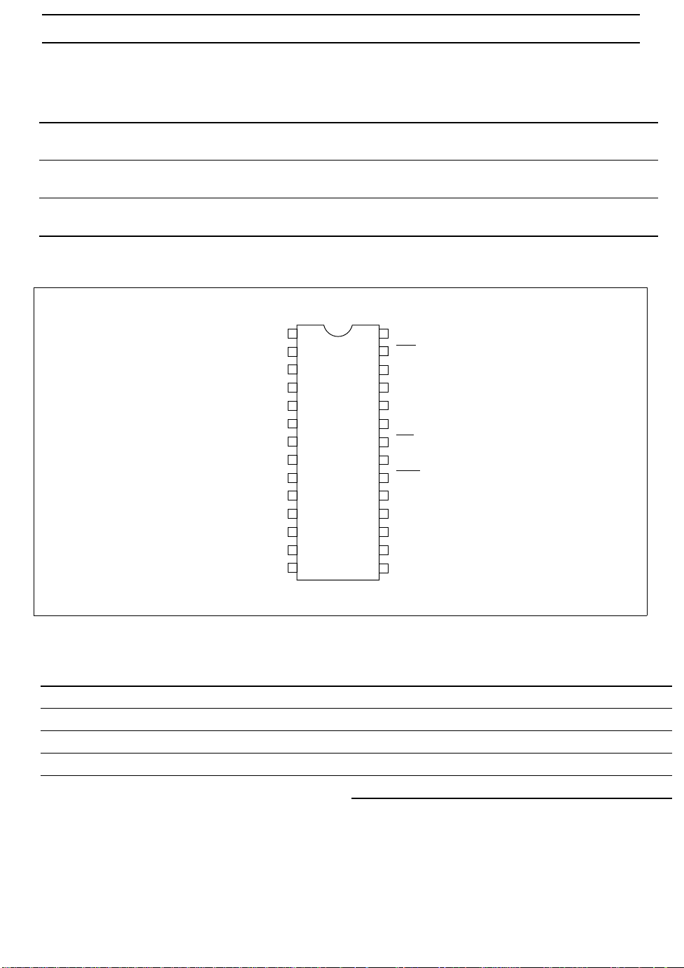
Pin Arrangement
85 ns
100 ns
85 ns
100 ns
85 ns
100 ns
600-mil, 28-pin plastic DIP (DP-28)
300-mil, 28-pin plastic DIP(DP-28N)
450-mil, 28-pin plastic SOP(FP-28DA)
HM6264BLP/BLSP/BLFP Series
1
NC
A12
A7
A6
A4
A0
I/O1
I/O2
I/O3
V
SS
2
3
4
5A5
6
7A3
8A2
9A1
10
11
12
13
14
28
27
24
23
22
21
20
19
18
V
CC
WE
CS226
A825
A9
A11
OE
A10
CS1
I/O8
I/O7
I/O617
I/O516
I/O415
(Top view)
Pin Description
Pin name Function Pin name Function
A0 to A12 Address input WE Write enable
I/O1 to I/O8 Data input/output OE Output enable
CS1 Chip select 1 NC No connection
CS2 Chip select 2 V
CC
V
SS
Power supply
Ground
Page 3
Block Diagram
A11
A8
A9
A7
A12
A5
A6
A4
Row
decoder
Memory array
256 × 256
HM6264B Series
V
CC
V
SS
I/O1
I/O8
CS2
CS1
WE
OE
Column I/O
Input
data
control
Timing pulse generator
Read, Write control
Column decoder
A1 A3
A2 A0 A10
Page 4

HM6264B Series
Function Table
WE CS1 CS2 OE Mode VCC current I/O pin Ref. cycle
× H ××Not selected (power down) I
××L × Not selected (power down) ISB, I
H L H H Output disable I
H L H L Read I
L L H H Write I
L L H L Write I
, I
SB
SB1
SB1
CC
CC
CC
CC
Note: ×: H or L
Absolute Maximum Ratings
Parameter Symbol Value Unit
Power supply voltage
Terminal voltage
*1
*1
Power dissipation P
Operating temperature Topr 0 to + 70 °C
Storage temperature Tstg –55 to +125 °C
Storage temperature under bias Tbias –10 to +85 °C
Notes: 1. Relative to V
SS
2. VT min: –3.0 V for pulse half-width ≤ 50 ns
3. Maximum voltage is 7.0 V
V
CC
V
T
T
–0.5 to +7.0 V
–0.5*2 to VCC + 0.3*3V
1.0 W
High-Z —
High-Z —
High-Z —
Dout Read cycle (1)–(3)
Din Write cycle (1)
Din Write cycle (2)
Recommended DC Operating Conditions (Ta = 0 to +70°C)
Parameter Symbol Min Typ Max Unit
Supply voltage V
Input high voltage V
Input low voltage V
CC
V
SS
IH
IL
Note: 1. VIL min: –3.0 V for pulse half-width ≤ 50 ns
4.5 5.0 5.5 V
000V
2.2 — VCC + 0.3 V
*1
–0.3
— 0.8 V
Page 5

HM6264B Series
DC Characteristics (Ta = 0 to +70°C, VCC = 5 V ±10%, VSS = 0 V)
Parameter Symbol Min Typ*1Max Unit Test conditions
Input leakage current |I
Output leakage current |ILO| ——2 µA CS1 = VIH or CS2 = VIL or OE = VIH or
Operating power supply
current
Average operating power
supply current
Standby power supply
current
Output low voltage V
Output high voltage V
Notes: 1. Typical values are at VCC = 5.0 V, Ta = +25°C and not guaranteed.
| ——2 µA Vin = VSS to V
LI
WE = V
I
CCDC
— 7 15 mA CS1 = VIL, CS2 = VIH, I
others = V
I
CC1
— 30 45 mA Min cycle, duty = 100%,
CS1 = V
others = V
I
CC2
— 3 5 mA Cycle time = 1 µs, duty = 100%, I
CS1 ≤ 0.2 V, CS2 ≥ V
V
≥ VCC – 0.2 V, VIL ≤ 0.2 V
IH
I
SB
I
SB1
—13mACS1 = VIH, CS2 = V
—2 50µA CS1 ≥ VCC – 0.2 V, CS2 ≥ VCC – 0.2 V or
0 V ≤ CS2 ≤ 0.2 V, 0 V ≤ Vin
OL
OH
— — 0.4 V IOL = 2.1 mA
2.4 — — V IOH = –1.0 mA
CC
, V
= V
IL
I/O
IH/VIL
, CS2 = VIH, I
IL
IH/VIL
SS
to V
CC
IL
CC
= 0 mA
I/O
= 0 mA
I/O
– 0.2 V,
= 0 mA
I/O
Capacitance (Ta = 25°C, f = 1.0 MHz)
Parameter Symbol Min Typ Max Unit Test conditions
Input capacitance
Input/output capacitance
*1
*1
Note: 1. This parameter is sampled and not 100% tested.
Cin — — 5 pF Vin = 0 V
C
I/O
——7 pFV
= 0 V
I/O
Page 6

HM6264B Series
AC Characteristics (Ta = 0 to +70°C, VCC = 5 V ± 10%, unless otherwise noted.)
Test Conditions
• Input pulse levels: 0.8 V to 2.4 V
• Input and output timing reference level: 1.5 V
• Input rise and fall time: 10 ns
• Output load: 1 TTL Gate + CL (100 pF) (Including scope & jig)
Read Cycle
HM6264B-8L HM6264B-10L
Parameter Symbol Min Max Min Max Unit Notes
Read cycle time t
Address access time t
Chip select access time CS1 t
CS2 t
Output enable to output valid t
Chip selection to output in low-Z CS1 t
CS2 t
Output enable to output in low-Z t
Chip deselection in to output in high-Z CS1 t
CS2 t
Output disable to output in high-Z t
Output hold from address change t
RC
AA
CO1
CO2
OE
LZ1
LZ2
OLZ
HZ1
HZ2
OHZ
OH
Notes: 1. tHZ is defined as the time at which the outputs achieve the open circuit conditions and are not
referred to output voltage levels.
2. At any given temperature and voltage condition, t
a given device and from device to device.
85 — 100 — ns
— 85 — 100 ns
— 85 — 100 ns
— 85 — 100 ns
— 45 — 50 ns
10 — 10 — ns 2
10 — 10 — ns 2
5—5—ns2
0 30 0 35 ns 1, 2
0 30 0 35 ns 1, 2
0 30 0 35 ns 1, 2
10 — 10 — ns
maximum is less than tLZ minimum both for
HZ
Page 7

Read Timing Waveform (1) (WE = VIH)
HM6264B Series
t
RC
Address
Valid address
t
AA
t
CO1
CS1
t
LZ1
t
CO2
CS2
t
LZ2
t
OE
Dout
High Impedance
Read Timing Waveform (2) (WE = VIH, OE = VIL)
Address
t
OH
Valid address
t
AA
OLZ
t
HZ1
t
OE
t
HZ2
t
OHZ
Valid data
t
OH
t
OH
Dout
Valid data
Page 8

HM6264B Series
Read Timing Waveform (3) (WE = VIH, OE = VIL)
t
CO1
*1
CS1
t
HZ1
t
LZ1
t
CS2
Dout
t
LZ2
t
CO2
Valid data
HZ2
Note: 1. Address must be valid prior to or simultaneously with CS1 going low or CS2 going high.
Page 9

HM6264B Series
Write Cycle
HM6264B-8L HM6264B-10L
Parameter Symbol Min Max Min Max Unit Notes
Write cycle time t
Chip selection to end of write t
Address setup time t
Address valid to end of write t
Write pulse width t
Write recovery time t
WE to output in high-Z t
Data to write time overlap t
Data hold from write time t
Output active from end of write t
Output disable to output in high-Z t
WC
CW
AS
AW
WP
WR
WHZ
DW
DH
OW
OHZ
Notes: 1. A write occurs during the overlap of a low CS1, and high CS2, and a high WE. A write begins
at the latest transition among CS1 going low,CS2 going high and WE going low. A write ends
at the earliest transition among CS1 going high CS2 going low and WE going high. Time t
measured from the beginning of write to the end of write.
2. t
is measured from the later of CS1 going low or CS2 going high to the end of write.
CW
3. t
is measured from the address valid to the beginning of write.
AS
4. t
is measured from the earliest of CS1 or WE going high or CS2 going low to the end of write
WR
cycle.
5. During this period, I/O pins are in the output state, therefore the input signals of the opposite
phase to the outputs must not be applied.
6. In the write cycle with OE low fixed, t
must satisfy the following equation to avoid a problem
WP
of data bus contention
≥ t
t
WP
max + tDW min.
WHZ
85 — 100 — ns
75 — 80 — ns 2
0—0—ns3
75 — 80 — ns
55 — 60 — ns 1, 6
0—0—ns4
0 30 0 35 ns 5
40 — 40 — ns
0—0—ns
5—5—ns
0 30 0 35 ns 5
is
WP
Page 10

HM6264B Series
Write Timing Waveform (1) (OE Clock)
t
WC
Address
OE
Valid address
t
CW
t
WR
CS1
*1
CS2
WE
Dout
Din
t
AS
High Impedance
t
AW
t
OHZ
t
WP
t
DW
High Impedance
t
DH
Valid data
Note: 1. If CS1 goes low or CS2 goes high simultaneously with WE going low or after WE going
low, the outputs remain in the high impedance state.
Page 11

Write Timing Waveform (2) (OE Low Fixed) (OE = VIL)
t
WC
HM6264B Series
Address
Valid address
t
AW
t
CW
t
WR
CS1
*1
CS2
t
WP
t
WHZ
t
DW
Valid data
t
OH
t
OW
*2
t
DH
*4
*3
WE
Dout
Din
t
AS
High Impedance
Notes: 1. If CS1 goes low simultaneously with WE going low or after WE goes low, the outputs
remain in high impedance state.
2. Dout is the same phase of the written data in this write cycle.
3. Dout is the read data of the next address.
4. If CS1 is low and CS2 is high during this period, I/O pins are in the output state. Input
signals of opposite phase to the outputs must not be applied to I/O pins.
Page 12

HM6264B Series
Low VCC Data Retention Characteristics (Ta = 0 to +70°C)
Parameter Symbol Min Typ*1Max Unit Test conditions
VCC for data retention V
Data retention current I
DR
CCDR
2.0 — — V CS1 ≥ VCC –0.2 V,
—1*125
CS2 ≥ V
*2
µAVCC = 3.0 V, 0 V ≤ Vin ≤ V
–0.2 V or CS2 ≤ 0.2 V
CC
CS1 ≥ VCC –0.2 V, CS2 ≥ VCC –0.2 V
or 0 V ≤ CS2 ≤ 0.2 V
Chip deselect to data
t
CDR
0 — — ns See retention waveform
retention time
Operation recovery time t
R
*3
t
RC
——ns
Notes: 1. Reference data at Ta = 25°C.
2. 10 µA max at Ta = 0 to + 40°C.
3. t
= read cycle time.
RC
4. CS2 controls address buffer, WE buffer, CS1 buffer, OE buffer, and Din buffer. If CS2 controls
data retention mode, Vin levels (address, WE, OE, CS1, I/O) can be in the high impedance
state. If CS1 controls data retention mode, CS2 must be CS2 ≥ V
– 0.2 V or 0 V ≤ CS2 ≤ 0.2
CC
V. The other input levels (address, WE, OE, I/O) can be in the high impedance state.
Low VCC Data Retention Timing Waveform (1) (CS1 Controlled)
V
CC
4.5 V
t
CDR
Data retention mode
t
R
*4
CC
2.2 V
V
DR
CS1
0 V
CS1 ≥ VCC – 0.2 V
Low VCC Data Retention Timing Waveform (2) (CS2 Controlled)
V
CC
4.5 V
CS2
V
DR
0.4 V
0 V
t
CDR
Data retention mode
CS2 ≤ 0.2 V
t
R
Page 13

HM6264B Series
Package Dimensions
HM6264BLP Series (DP-28) Unit: mm
35.6
28
36.5 Max
15
13.4
14.6 Max
1
1.9 Max
2.54 ± 0.25
1.2
0.48 ± 0.10
14
5.7 Max
2.54 Min
0.51 Min
0° – 15°
15.24
0.25
+ 0.11
– 0.05
Page 14

HM6264B Series
HM6264BLSP Series (DP-28N) Unit: mm
36.00
28
37.32 Max
114
1.30
15
6.60
7.00 Max
2.20 Max
7.62
5.08 Max
+ 0.11
0.25
2.54 ± 0.25
0.48 ± 0.10
2.54 Min
0.51 Min
0° – 15°
– 0.05
HM6264BLTM Series (FP-28DA) Unit: mm
18.3
18.75 Max
+ 0.10
– 0.05
14
15
8.4
3.0 Max
0.1 Min
+ 0.08
– 0.07
0.17
11.8 ± 0.3
0 – 10 °
1.0
28
1
0.895
1.27 ± 0.10
0.40
Page 15

HM6264B Series
When using this document, keep the following in mind:
1. This document may, wholly or partially, be subject to change without notice.
2. All rights are reserved: No one is permitted to reproduce or duplicate, in any form, the whole or part
of this document without Hitachi’s permission.
3. Hitachi will not be held responsible for any damage to the user that may result from accidents or any
other reasons during operation of the user’s unit according to this document.
4. Circuitry and other examples described herein are meant merely to indicate the characteristics and
performance of Hitachi’s semiconductor products. Hitachi assumes no responsibility for any
intellectual property claims or other problems that may result from applications based on the examples
described herein.
5. No license is granted by implication or otherwise under any patents or other rights of any third party
or Hitachi, Ltd.
6. MEDICAL APPLICATIONS: Hitachi’s products are not authorized for use in MEDICAL
APPLICATIONS without the written consent of the appropriate officer of Hitachi’s sales company.
Such use includes, but is not limited to, use in life support systems. Buyers of Hitachi’s products are
requested to notify the relevant Hitachi sales offices when planning to use the products in MEDICAL
APPLICATIONS.
Hitachi, Ltd.
Semiconductor & IC Div.
Nippon Bldg., 2-6-2, Ohte-machi, Chiyoda-ku, Tokyo 100, Japan
Tel: Tokyo (03) 3270-2111
Fax: (03) 3270-5109
For further information write to:
Hitachi America, Ltd.
Semiconductor & IC Div.
2000 Sierra Point Parkway
Brisbane, CA. 94005-1835
U S A
Tel: 415-589-8300
Fax: 415-583-4207
Hitachi Europe GmbH
Electronic Components Group
Continental Europe
Dornacher Straße 3
D-85622 Feldkirchen
München
Tel: 089-9 91 80-0
Fax: 089-9 29 30 00
Hitachi Europe Ltd.
Electronic Components Div.
Northern Europe Headquarters
Whitebrook Park
Lower Cookham Road
Maidenhead
Berkshire SL6 8YA
United Kingdom
Tel: 0628-585000
Fax: 0628-778322
Hitachi Asia Pte. Ltd.
16 Collyer Quay #20-00
Hitachi Tower
Singapore 0104
Tel: 535-2100
Fax: 535-1533
Hitachi Asia (Hong Kong) Ltd.
Unit 706, North Tower,
World Finance Centre,
Harbour City, Canton Road
Tsim Sha Tsui, Kowloon
Hong Kong
Tel: 27359218
Fax: 27306071
 Loading...