

Page 1
HM5225645F-B60
HM5225325F-B60
256M LVTTL interface SDRAM
100 MHz
1-Mword × 64-bit × 4-bank/2-Mword × 32-bit × 4-bank
PC/100 SDRAM
ADE-203-1014C (Z)
Rev. 1.0
Oct. 1, 1999
Description
The Hitachi HM5225645F is a 256-Mbit SDRAM organized as 1048576-word × 64-bit × 4-bank. The Hitachi
HM5225325F is a 256-Mbit SDRAM organized as 2097152-word × 32-bit × 4-bank. All inputs and outputs
are referred to the rising edge of the clock input. It is packaged in standard 108 bump BGA.
Features
• Single chip wide bit solution (× 64/× 32)
• 3.3 V power supply
• Clock frequency: 100 MHz (max)
• LVTTL interface
• Extremely small foot print: 1.27 mm pitch
Package: BGA (BP-108)
• 4 banks can operate simultaneously and independently
• Burst read/write operation and burst read/single write operation capability
• Programmable burst length: 4/8/full page
• 2 variations of burst sequence
Sequential (BL = 4/8/full page)
Interleave (BL = 4/8)
• Programmable CAS latency: 2/3
• Byte control by DQMB
Page 2

HM5225645F-B60, HM5225325F-B60
• Refresh cycles: 4096 refresh cycles/64 ms
• 2 variations of refresh
Auto refresh
Self refresh
• Full page burst length capability
Sequential burst
Burst stop capability
Ordering Information
Type No. Frequency CAS latency Package
HM5225645FBP-B60* 100 MHz 3 14 mm × 22 mm 108 bump BGA (BP-108)
HM5225325FBP-B60* 100 MHz 3
Note: 66 MHz operation at CAS latency = 2.
2
Page 3
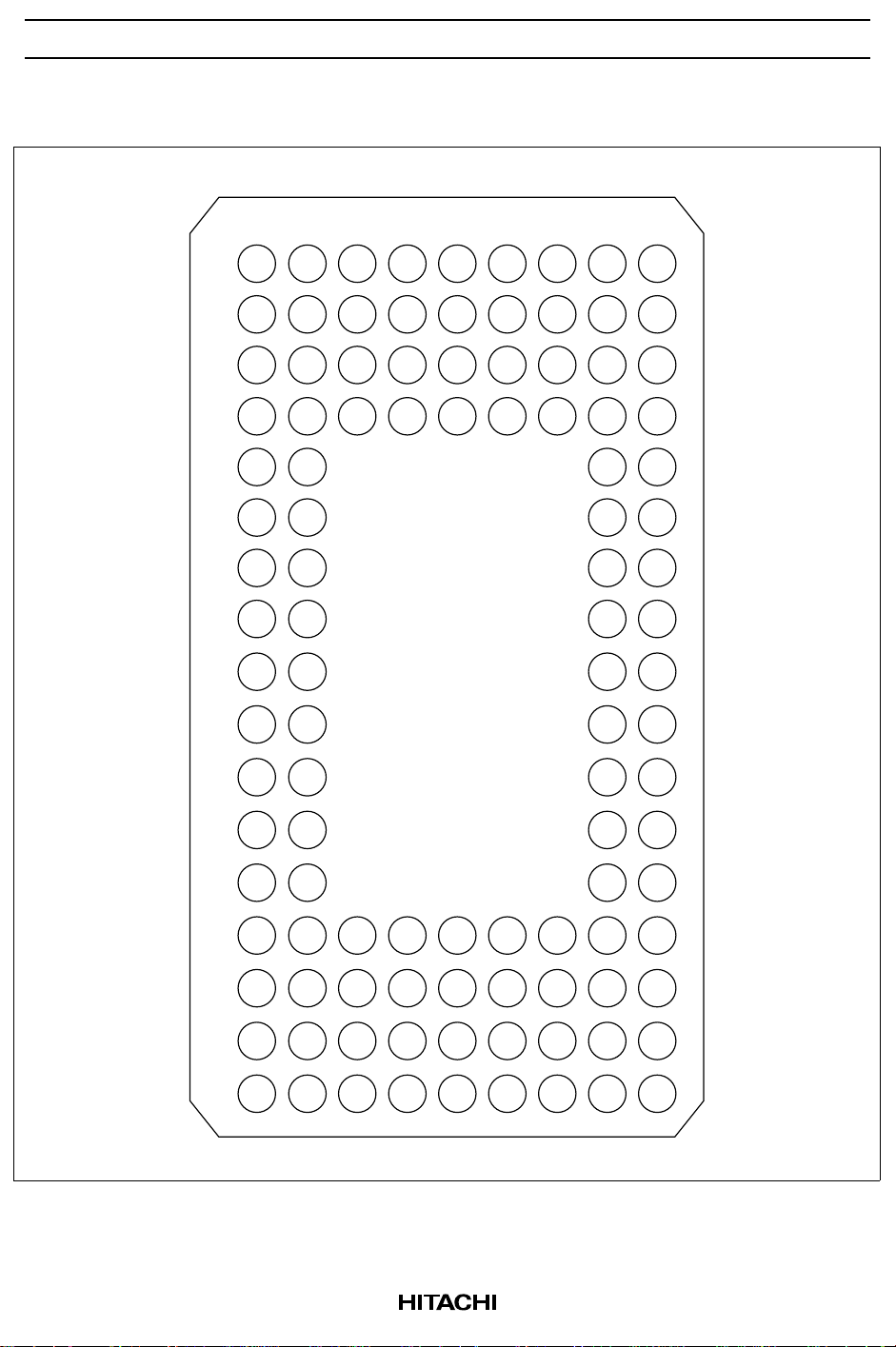
Pin Arrangement (HM5225645F)
1 2 3 4 5 6 7 8 9
HM5225645F-B60, HM5225325F-B60
108-bump BGA
DQ50
DQ52
DQ54
V
SS
V
CC
V
CC
V
SS
DQ47
DQ45
DQ43
DQ41
DQ46
DQ44
DQ42
DQ40
DQ33
DQ35
DQ37
DQ39
DQ
MB5
RAS
A10
V
CC
A2
V
SS
A9 CS
DQ32
DQ34
DQ36
DQ38
DQ
MB4
WE
A13
A1
A3
A0
A
DQ63
DQ62
DQ49 DQ48
DQ61
DQ60
DQ58
DQ56
DQ
MB6
V
CC
V
CC
A5
V
SS
A6
V
SS
DQ51
DQ53
DQ55
B
C
DQ59
DQ57
D
DQ
E
MB7
F
CKE
A12
G
A7
H
A4
J
A8
K
A11
L
Open CLK V
M
DQ
N
MB0DQMB1
DQ6 DQ7 DQ8 DQ9 VSSDQ22 DQ23 DQ24 DQ25
P
DQ4 DQ5 DQ10 DQ11 VCCDQ20 DQ21 DQ26 DQ27
R
DQ2 DQ3 DQ12 DQ13 VCCDQ18 DQ19 DQ28 DQ29
T
DQ0 DQ1 DQ14 DQ15 V
U
SS
DQ16
MB2DQMB3
DQ17 DQ30 DQ31
(Top view)
DQ
CAS
CC
3
Page 4
HM5225645F-B60, HM5225325F-B60
Pin Description (HM5225645F)
Pin name Function
A0 to A13 Address input
Row address A0 to A11
Column address A0 to A7
Bank select address A12/A13 (BS)
DQ0 to DQ63 Data-input/output
CS Chip select
RAS Row address strobe command
CAS Column address strobe command
WE Write enable
DQMB0 to DQMB7 Byte data mask*
CLK Clock input
CKE Clock enable
V
CC
V
SS
Open Open*
Power supply
Ground
2
Note: 1. DQMB0: DQ0 to DQ7
DQMB1: DQ8 to DQ15
DQMB2: DQ16 to DQ23
DQMB3: DQ24 to DQ31
DQMB4: DQ32 to DQ39
DQMB5: DQ40 to DQ47
DQMB6: DQ48 to DQ55
DQMB7: DQ56 to DQ63
2. Don’t connect. Internally connected with die.
1
4
Page 5
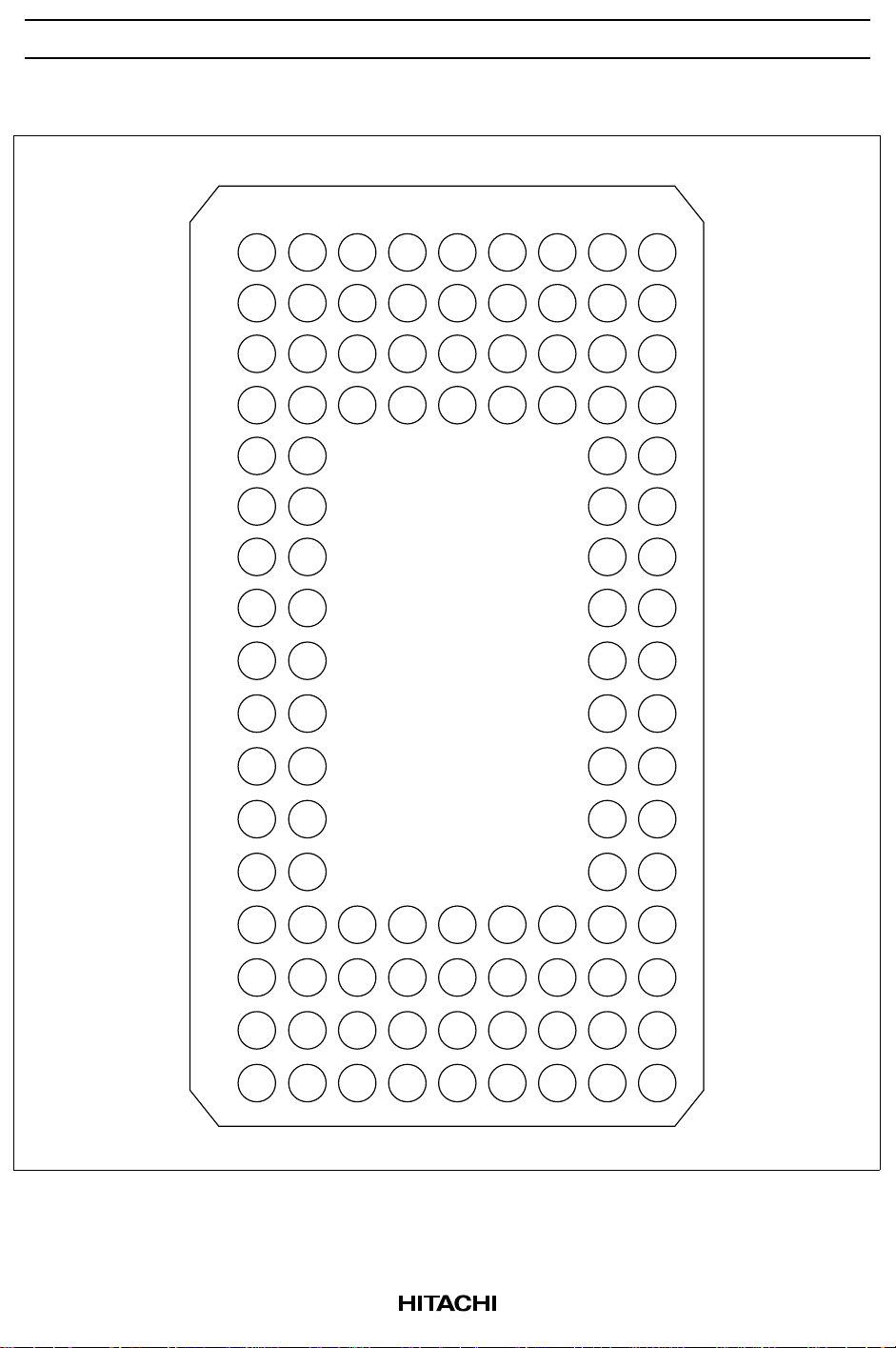
Pin Arrangement (HM5225325F)
1 2 3 4 5 6 7 8 9
HM5225645F-B60, HM5225325F-B60
108-bump BGA
DQ25
DQ26
DQ27
V
SS
DQ23
V
DQ22
CC
DQ21
V
CC
DQ20
V
SS
NC
NC
NC
NC
NC
DQ16
NC
DQ17
NC
DQ18
NC
DQ19
DQ
MB2
RAS
A10
V
CC
A2
V
SS
A9 CS
NC
WE
A13
A1
A3
A0
A
DQ31
DQ30
B
C
DQ29
DQ28
D
E
F
G
H
J
K
L
DQ
MB3
CKE
A12
A7
A4
A8
A11
NC
NC
NC
NC
NC
V
V
A5
V
A6
V
NC DQ24
NC
NC
NC
CC
CC
SS
SS
Open CLK V
M
DQ
NC
N
P
R
T
U
MB0
DQ3 NC NC DQ4 VSSDQ11 NC NC DQ12
DQ2 NC NC DQ5 VCCDQ10 NC NC DQ13
DQ1 NC NC DQ6 V
DQ0 NC NC DQ7 V
DQ9 NC NC DQ14
CC
DQ8
SS
NC NC DQ15
(Top view)
NC
CAS
CC
DQ
MB1
5
Page 6

HM5225645F-B60, HM5225325F-B60
Pin Description (HM5225325F)
Pin name Function
A0 to A13 Address input
Row address A0 to A11
Column address A0 to A8
Bank select address A12/A13 (BS)
DQ0 to DQ31 Data-input/output
CS Chip select
RAS Row address strobe command
CAS Column address strobe command
WE Write enable
DQMB0 to DQMB3 Byte data mask*
CLK Clock input
CKE Clock enable
V
CC
V
SS
Open Open*
Power supply
Ground
2
NC No connection*
Note: 1. DQMB0: DQ0 to DQ7
DQMB1: DQ8 to DQ15
DQMB2: DQ16 to DQ23
DQMB3: DQ24 to DQ31
2. Don’t connect. Internally connected with die.
3. Not internally connected with die.
1
3
6
Page 7

Block Diagram (HM5225645F)
HM5225645F-B60, HM5225325F-B60
CS
RAS
CAS
WE
CLK
CKE
14
64-Mbit SDRAM
4M × 16
2
8
64
16
A0 to A13
DQMB 0 to
DQMB 7
DQ 0 to DQ 63
Block Diagram (HM5225325F)
64-Mbit SDRAM
4M × 16
216
64-Mbit SDRAM
4M × 16
216
64-Mbit SDRAM
4M × 16
216
A0 to A13
CS
RAS
CAS
WE
CLK
CKE
DQMB 0 to
DQMB 3
DQ 0 to DQ 31
14
64-Mbit SDRAM
8M × 8
1
4
32
64-Mbit SDRAM
8M × 8
8
18
64-Mbit SDRAM
8M × 8
18
64-Mbit SDRAM
8M × 8
18
7
Page 8

HM5225645F-B60, HM5225325F-B60
Power-up Sequence and Initialization Sequence
Initialization sequence
200 µs
V
CC
CKE, DQMB
CLK
CS, DQ
Power up sequence
100 µs
0 V
Low
Low
Low
Power stabilize
Absolute Maximum Ratings
Parameter Symbol Value Unit Note
Voltage on any pin relative to V
Supply voltage relative to V
SS
SS
V
T
V
CC
Short circuit output current Iout 50 mA
Operating temperature Topr 0 to +70 (Tj max = 110) °C
Storage temperature Tstg –55 to +125 °C
Note: 1. Respect to V
SS
–0.5 to VCC + 0.5
V1
(≤ 4.6 (max))
–0.5 to +4.6 V 1
DC Operating Conditions (Tcase = 0 to +70°C [Tj max = 110°C])
Parameter Symbol Min Max Unit Notes
Supply voltage V
Input high voltage V
Input low voltage V
Notes: 1. All voltage referred to V
SS
2. The supply voltage with all V
3. The supply voltage with all V
4. V
(max) = VCC + 2.0 V for pulse width ≤ 3 ns at VCC.
IH
5. V
(min) = VSS – 2.0 V for pulse width ≤ 3 ns at VSS.
IL
8
CC
V
SS
IH
IL
pins must be on the same level.
CC
pins must be on the same level.
SS
3.0 3.6 V 1, 2
00 V3
2.0 VCC + 0.3 V 1, 4
–0.3 0.8 V 1, 5
Page 9

HM5225645F-B60, HM5225325F-B60
DC Characteristics
(Tcase = 0 to 70°C [Tj max = 110°C]), VCC = 3.3 V ± 0.3 V, VSS = 0 V) (HM5225645F)
HM5225645F
-B60
Parameter Symbol Min Max Unit Test conditions Notes
Operating current
(CAS latency = 2) I
(CAS latency = 3) I
Standby current in power down I
Standby current in power down
(input signal stable)
Standby current in non power
down
Standby current in non power
down (input signal stable)
Active standby current in power
down
Active standby current in power
down (input signal stable)
Active standby current in non
power down
Active standby current in non
power down (input signal stable)
Burst operating current
(CAS latency = 2) I
(CAS latency = 3) I
Refresh current I
Self refresh current I
Self refresh current (L-version) I
Input leakage current I
Output leakage current I
Output high voltage V
Output low voltage V
CC1
CC1
CC2P
I
CC2PS
I
CC2N
I
CC2NS
I
CC3P
I
CC3PS
I
CC3N
I
CC3NS
CC4
CC4
CC5
CC6
CC6
LI
LO
— 200 mA
— 220 mA
— 12 mA CKE = VIL,
— 8 mA CKE = VIL, tCK = ∞ 7
— 64 mA CKE, CS = VIH,
— 36 mA CKE = VIH, tCK = ∞ 9
— 16 mA CKE = VIL,
— 12 mA CKE = VIL, tCK = ∞ 2, 7
— 80 mA CKE, CS = VIH,
— 60 mA CKE = VIH, tCK = ∞ 2, 9
— 220 mA tCK = min, BL = 4 1, 2, 5
— 270 mA
— 380 mA tRC = min 3
— 4 mA VIH ≥ VCC – 0.2 V
— 1.6 mA
–4 4 µA0 ≤ Vin ≤ V
–6 6 µA0 ≤ Vout ≤ V
OH
OL
2.4 — V IOH = –4 mA
— 0.4 V IOL = 4 mA
Burst length = 1
tRC = min
t
= 12 ns
CK
t
= 12 ns
CK
t
= 12 ns
CK
t
= 12 ns
CK
V
≤ 0.2 V
IL
CC
CC
DQ = disable
1, 2, 3
6
4
1, 2, 6
1, 2, 4
8
9
Page 10

HM5225645F-B60, HM5225325F-B60
DC Characteristics
(Tcase = 0 to 70°C [Tj max = 110°C]), VCC = 3.3 V ± 0.3 V, VSS = 0 V) (HM5225325F)
HM5225325F
-B60
Parameter Symbol Min Max Unit Test conditions Notes
Operating current
(CAS latency = 2) I
(CAS latency = 3) I
Standby current in power down I
Standby current in power down
(input signal stable)
Standby current in non power
down
Standby current in non power
down (input signal stable)
Active standby current in power
down
Active standby current in power
down (input signal stable)
Active standby current in non
power down
Active standby current in non
power down (input signal stable)
Burst operating current
(CAS latency = 2) I
(CAS latency = 3) I
Refresh current I
Self refresh current I
Self refresh current (L-version) I
Input leakage current I
Output leakage current I
Output high voltage V
Output low voltage V
CC1
CC1
CC2P
I
CC2PS
I
CC2N
I
CC2NS
I
CC3P
I
CC3PS
I
CC3N
I
CC3NS
CC4
CC4
CC5
CC6
CC6
LI
LO
— 180 mA
— 200 mA
— 12 mA CKE = VIL,
— 8 mA CKE = VIL, tCK = ∞ 7
— 64 mA CKE, CS = VIH,
— 36 mA CKE = VIH, tCK = ∞ 9
— 16 mA CKE = VIL,
— 12 mA CKE = VIL, tCK = ∞ 2, 7
— 80 mA CKE, CS = VIH,
— 60 mA CKE = VIH, tCK = ∞ 2, 9
— 200 mA tCK = min, BL = 4 1, 2, 5
— 250 mA
— 380 mA tRC = min 3
— 4 mA VIH ≥ VCC – 0.2 V
— 1.6 mA
–4 4 µA0 ≤ Vin ≤ V
–6 6 µA0 ≤ Vout ≤ V
OH
OL
2.4 — V IOH = –4 mA
— 0.4 V IOL = 4 mA
Burst length = 1
tRC = min
t
= 12 ns
CK
t
= 12 ns
CK
t
= 12 ns
CK
t
= 12 ns
CK
V
≤ 0.2 V
IL
CC
CC
DQ = disable
1, 2, 3
6
4
1, 2, 6
1, 2, 4
8
10
Page 11

HM5225645F-B60, HM5225325F-B60
Notes: 1. ICC depends on output load condition when the device is selected. ICC (max) is specified at the
output open condition.
2. One bank operation.
3. Input signals are changed once per one clock.
4. Input signals are changed once per two clocks.
5. Input signals are changed once per four clocks.
6. After power down mode, CLK operating current.
7. After power down mode, no CLK operating current.
8. After self refresh mode set, self refresh current.
9. Input signals are V
Capacitance (Ta = 25°C, VCC = 3.3 V ± 0.3 V)
Parameter Symbol Min Max Unit Notes
Input capacitance (CLK) C
Input capacitance
(Input except DQM)
Input capacitance (DQM) C
Output capacitance (DQ) C
Notes: 1. Capacitance measured with Boonton Meter or effective capacitance measuring method.
2. Measurement condition: f = 1 MHz, 1.4 V bias, 200 mV swing.
3. DQMB = V
4. This parameter is sampled and not 100% tested.
to disable Dout.
IH
or VIL fixed.
IH
I1
C
I2
I3
O
10 14 pF 1, 2, 4
10 14 pF 1, 2, 4
2.5 5 pF 1, 2, 4
3 5 pF 1, 2, 3, 4
11
Page 12

HM5225645F-B60, HM5225325F-B60
AC Characteristics
(Tcase = 0 to 70°C [Tj max = 110°C]), VCC = 3.3 V ± 0.3 V, VSS = 0 V)
HM5225645F/HM5225325F
-B60
HITACHI
Parameter
Symbol
System clock cycle time
(CAS latency = 2) t
(CAS latency = 3) t
CLK high pulse width t
CLK low pulse width t
CK
CK
CKH
CKL
Access time from CLK
(CAS latency = 2) t
(CAS latency = 3) t
Data-out hold time t
CLK to Data-out low impedance t
CLK to Data-out high impedance
AC
AC
OH
LZ
t
HZ
(CAS latency = 2, 3)
Input setup time tAS, tCS, tDS,
t
CES
CKE setup time for power down
t
CESP
exit
Input hold time tAH, tCH, tDH,
t
CEH
Ref/Active to Ref/Active command
t
RC
period
Active to Precharge command
t
RAS
period
Active command to column
t
RCD
command (same bank)
Precharge to active command
t
RP
period
Write recovery or data-in to
t
DPL
precharge lead time
Active (a) to Active (b) command
t
RRD
period
Transition time (rise and fall) t
Refresh period t
T
REF
PC/100
Symbol Min Max Unit Notes
Tclk 15 — ns 1
Tclk 10 — ns
Tch 3 — ns 1
Tcl 3 — ns 1
Tac — 8 ns 1, 2
Tac — 6 ns
Toh 3 — ns 1, 2
2 — ns 1, 2, 3
— 6 ns 1, 4
Tsi 2 — ns 1, 5, 6
Tpde 2 — ns 1
Thi 1 — ns 1, 5
Trc 70 — ns 1
Tras 50 120000 ns 1
Trcd 20 — ns 1
Trp 20 — ns 1
Tdpl 10 — ns 1
Trrd 20 — ns 1
15ns
—64ms
12
Page 13

HM5225645F-B60, HM5225325F-B60
Notes: 1. AC measurement assumes tT = 1 ns. Reference level for timing of input signals is 1.5 V.
2. Access time is measured at 1.5 V. Load condition is CL = 50 pF.
(min) defines the time at which the outputs achieves the low impedance state.
3. t
LZ
4. t
(max) defines the time at which the outputs achieves the high impedance state.
HZ
5. t
define CKE setup time to CLK rising edge except power down exit command.
CES
6. t
Test Conditions
• Input and output timing reference levels: 1.5 V
• Input waveform and output load: See following figures
: Address, tCS/tCH: CS, RAS, CAS , WE, DQM.
AS/tAH
t
DS/tDH
: Data-in, t
CES/tCEH
: CKE
input
2.4 V
0.4 V
2.0 V
0.8 V
I/O
CL
t
T
t
T
13
Page 14

HM5225645F-B60, HM5225325F-B60
Package Dimensions
HM5225645FBP Series
HM5225325FBP Series (BP-108)
Preliminary
Pin 1 Index
4×C1.2
22.00
-B-
14.00
13.0 ± 0.10
0.20
4×
-A-
C
0.35
21.0 ± 0.10
-C-
C
0.15
1.27
1.27
123456798
Unit: mm
A
A
B
C
D
E
F
G
H
J
K
L
M
N
P
R
T
U
14
0.60
108× φ0.75
φ0.30
M
φ0.15
M
AB
C
C
Details of the part A
2.10
2.35 Max
Hitachi Code
JEDEC
EIAJ
Weight
(reference value)
BP-108
—
—
1.2 g
Page 15

HM5225645F-B60, HM5225325F-B60
Cautions
1. Hitachi neither warrants nor grants licenses of any rights of Hitachi’s or any third party’s patent,
copyright, trademark, or other intellectual property rights for information contained in this document.
Hitachi bears no responsibility for problems that may arise with third party’s rights, including intellectual
property rights, in connection with use of the information contained in this document.
2. Products and product specifications may be subject to change without notice. Confirm that you have
received the latest product standards or specifications before final design, purchase or use.
3. Hitachi makes every attempt to ensure that its products are of high quality and reliability. However,
contact Hitachi’s sales office before using the product in an application that demands especially high
quality and reliability or where its failure or malfunction may directly threaten human life or cause risk of
bodily injury, such as aerospace, aeronautics, nuclear power, combustion control, transportation, traffic,
safety equipment or medical equipment for life support.
4. Design your application so that the product is used within the ranges guaranteed by Hitachi particularly for
maximum rating, operating supply voltage range, heat radiation characteristics, installation conditions and
other characteristics. Hitachi bears no responsibility for failure or damage when used beyond the
guaranteed ranges. Even within the guaranteed ranges, consider normally foreseeable failure rates or
failure modes in semiconductor devices and employ systemic measures such as fail-safes, so that the
equipment incorporating Hitachi product does not cause bodily injury, fire or other consequential damage
due to operation of the Hitachi product.
5. This product is not designed to be radiation resistant.
6. No one is permitted to reproduce or duplicate, in any form, the whole or part of this document without
written approval from Hitachi.
7. Contact Hitachi’s sales office for any questions regarding this document or Hitachi semiconductor
products.
Hitachi, Ltd.
Semiconductor & Integrated Circuits.
Nippon Bldg., 2-6-2, Ohte-machi, Chiyoda-ku, Tokyo 100-0004, Japan
Tel: Tokyo (03) 3270-2111 Fax: (03) 3270-5109
URL NorthAmerica : http:semiconductor.hitachi.com/
For further information write to:
Hitachi Semiconductor
(America) Inc.
179 East Tasman Drive,
San Jose,CA 95134
Tel: <1> (408) 433-1990
Fax: <1>(408) 433-0223
Europe : http://www.hitachi-eu.com/hel/ecg
Asia (Singapore) : http://www.has.hitachi.com.sg/grp3/sicd/index.htm
Asia (Taiwan) : http://www.hitachi.com.tw/E/Product/SICD_Frame.htm
Asia (HongKong) : http://www.hitachi.com.hk/eng/bo/grp3/index.htm
Japan : http://www.hitachi.co.jp/Sicd/indx.htm
Hitachi Europe GmbH
Electronic components Group
Dornacher Straße 3
D-85622 Feldkirchen, Munich
Germany
Tel: <49> (89) 9 9180-0
Fax: <49> (89) 9 29 30 00
Hitachi Europe Ltd.
Electronic Components Group.
Whitebrook Park
Lower Cookham Road
Maidenhead
Berkshire SL6 8YA, United Kingdom
Tel: <44> (1628) 585000
Fax: <44> (1628) 778322
Hitachi Asia Pte. Ltd.
16 Collyer Quay #20-00
Hitachi Tower
Singapore 049318
Tel: 535-2100
Fax: 535-1533
Hitachi Asia Ltd.
Taipei Branch Office
3F, Hung Kuo Building. No.167,
Tun-Hwa North Road, Taipei (105)
Tel: <886> (2) 2718-3666
Fax: <886> (2) 2718-8180
Copyright © Hitachi, Ltd., 1998. All rights reserved. Printed in Japan.
Hitachi Asia (Hong Kong) Ltd.
Group III (Electronic Components)
7/F., North Tower, World Finance Centre,
Harbour City, Canton Road, Tsim Sha Tsui,
Kowloon, Hong Kong
Tel: <852> (2) 735 9218
Fax: <852> (2) 730 0281
Telex: 40815 HITEC HX
15
Page 16

HM5225645F-B60, HM5225325F-B60
Revision Record
Rev. Date Contents of Modification Drawn by Approved by
0.0 Feb. 1, 1999 Initial issue S. Hatano S. Hatano
0.1 Feb. 19, 1999 Pin arrangement
Correct pin No. to JEDEC standard
Package dimenssion
Correct illustration and indexes
0.2 Apr. 1, 1999 Ordering information
Correct error of type No.
1.0 Oct. 1, 1999 Programmable CAS latency: 3 to 2/3
Ordering information
Addition of note
Pin description
Addition of note 1
DC Characteristics (HM5225645F)
max (CL = 2): 280 mA to 200 mA
I
CC1
I
max (CL = 3): 300 mA to 220 mA
CC1
I
max (CL = 2): 280 mA to 220 mA
CC4
I
max (CL = 3): 360 mA to 270 mA
CC4
I
max: 460 mA to 380 mA
CC5
DC Characteristics (HM5225325F)
max (CL = 2): 260 mA to 180 mA
I
CC1
I
max (CL = 3): 280 mA to 200 mA
CC1
I
max (CL = 2): 260 mA to 200 mA
CC4
I
max (CL = 3): 320 mA to 250 mA
CC4
I
max: 460 mA to 380 mA
CC5
Capacitance
max: 16 pF to 14 pF
C
I1
C
max: 20 pF to 14 pF
I2
C
min: 4 pF to 3 pF
O
C
max: 6.5 pF to 5 pF
O
Package dimension
Change tolerance of height
S. Hatano S. Hatano
S. Hatano S. Hatano
16
 Loading...