

Page 1
H L 1 4 1 0 4
LCD Driver
HL15604
Hyundai Electronics Industries
System IC Division
1
1
Page 2

Contents
1. General Description
2. Features
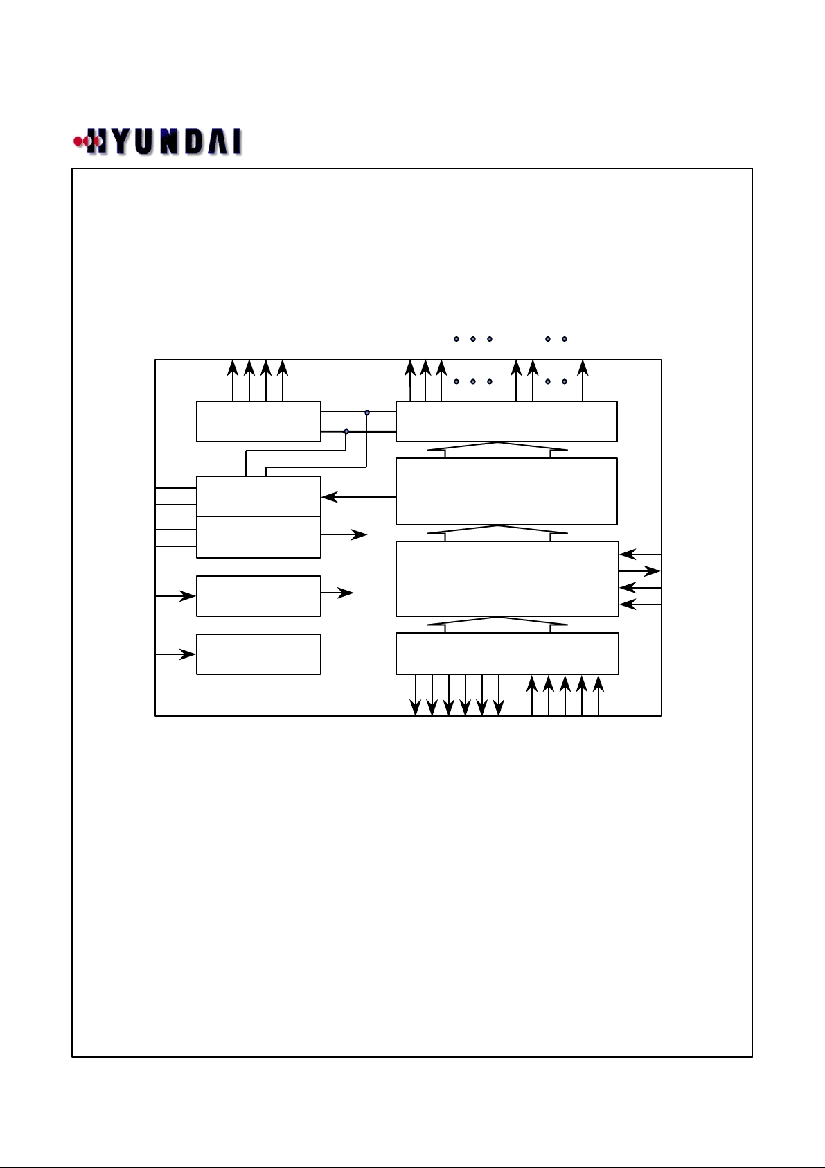
3. Block Diagram
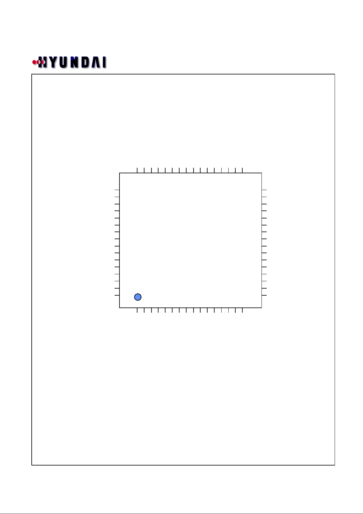
4. Pin Diagram
5. Pin Description
6. Serial I/O Data Format
7. Registers
HL15604
8. Key Scan Function
9. LCD Function
10. Power On Reset
11. Power Down Mode
12. Oscillator Port
13. Electrical Characteristics
14. Application
2
Page 3
HL15604
1. General Description
The HL14104 is 1/4 duty LCD display driver. It can drive directly maximum
164 segments. Also it has four general purpose output ports and a key scan
function that accepts input from up to 30 keys.
2. Features
• LCD display ..................................... 41 segments x 4 commons
1/4 duty - 1/2 bias
1/4 duty - 1/3 bias
• Key scan ............................................ Maximum 30 keys
Input 5 pins, Output 6 pins
• Power down mode ............................. Sleep mode and all segments off mode
• Port
Output .................................................. 4 pins
( Including the LCD segment port )
• Serial I/O .............................................. Data transfer and receive
• Power on reset ..................................... Supply voltage detection ( SVD )
• RC oscillator
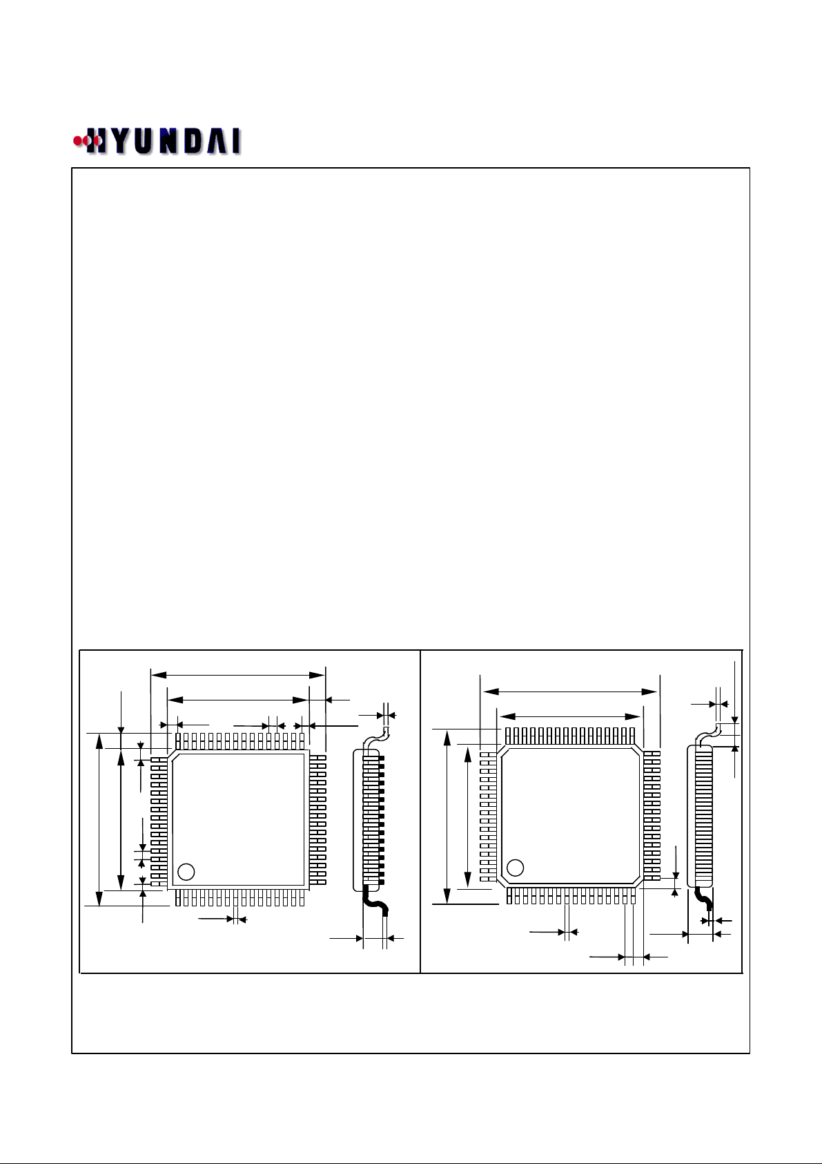
• Package ............................................... 64QFP
(1.6)
17.2
14.0
Unit : mm
Package Dimensions
64QFP (14×14)
17.2
14.0
1.0
0.8
1.0
48
49
64
1.0
1
0.8
0.35
16
33
32
17
(1.6)
1.0
0.15
64QFP (10×10)
12.0
10.0
48
49
12.0
10.0
64
1
0.12.7
Unit : mm
0.18
0.5
32
33
16
0.15
1.25
17
1.7max
1.25
0.5
0.5
0.1
3
Page 4
3. Block Diagram
COM4
COM3
COM2
COM1
KS1 / SEG40
SEG39
KS2 / SEG41
SEG5
SEG4 / P4
HL15604
SEG1 / P1
VCL1
VCL2
VDD
VSS
OSC
TEST
COMMOM
DRIVER
LCD
BIAS
SVD
CLOCK
GENERATOR
TEST
CONTROL
RESET
CLOCK
SEGMENT
DRIVER
LCD
DISPLAY & CONTROL
REGISTER
SERIAL
I/O
KEY
SCAN
KS6
KS5
KS4
KS3
KS2
KS1
KIN5
KIN4
KIN3
KIN2
SI
SO
SCK
CE
KIN1
4
Page 5
4. Pin Diagram
KS5
KS4
KS3
KS2 / SEG41
KS1 / SEG40
COM4
COM3
COM2
COM1
SEG39
SEG38
SEG37
SEG36
SEG35
SEG34
HL15604
SEG33
KS6
KIN1
KIN2
KIN3
KIN4
KIN5
TEST
VDD
VCL1
VCL2
VSS
OSC
SO
CE
SCK
484746454443424140393837363534
49
50
51
52
53
54
55
56
57
58
59
60
61
62
63
64
SI
123456789101112131415
SEG1 / P1
SEG2 / P2
HL14104
SEG5
SEG6
SEG3 / P3
SEG4 / P4
SEG7
SEG8
SEG9
SEG10
SEG11
SEG12
SEG13
SEG14
SEG15
33
32
31
30
29
28
27
26
25
24
23
22
21
20
19
18
17
16
SEG16
SEG32
SEG31
SEG30
SEG29
SEG28
SEG27
SEG26
SEG25
SEG24
SEG23
SEG22
SEG21
SEG20
SEG19
SEG18
SEG17
5
Page 6
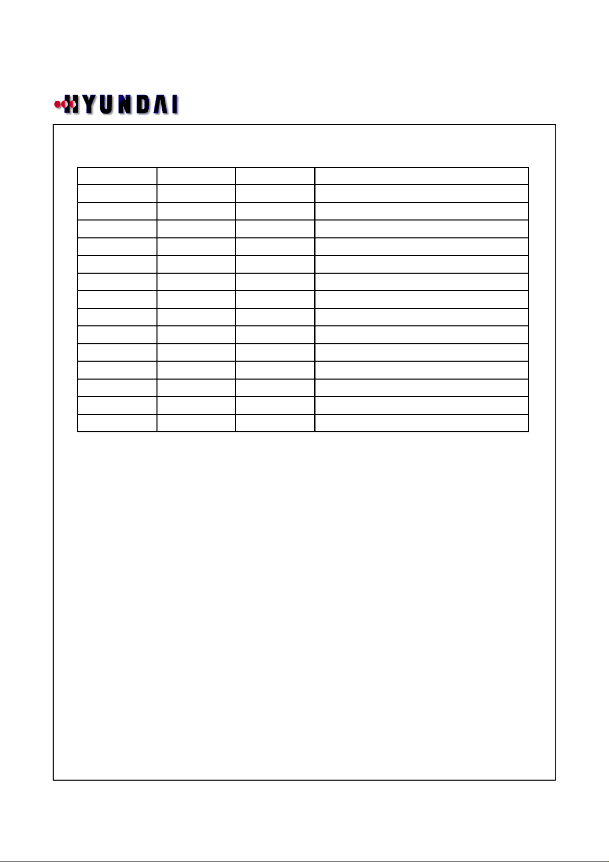
5. Pin Description
PIN Name I/O Pin Number Contents
SEG[41:1] O 41 LCD SEG Pins share P1,P2,P3 and P4
COM [4:1] O 4 LCD Common Pins
VCL[2:1] I 2 LCD Bias Pins
OSC I/O 1 Oscillator Input Pin
KS[6:1] O 6 Key Scan Output Pins
KIN[5:1] I 5 Key Scan Input Pins
CE I 1 Serial I/O Control Pin
SCK I 1 Serial I/O Clock Pin
SO O 1 Serial I/O Data Output Pin
SI I 1 Serial I/O Data Input Pin
TEST I 1 Test Pin. “1” Test mode , “0” Normal Mode
P[4:1] O 4 Output Port share SEG[4:1]
VDD I 1 Power Supply Pin
HL15604
VSS I 1 Ground Pin
6
Page 7
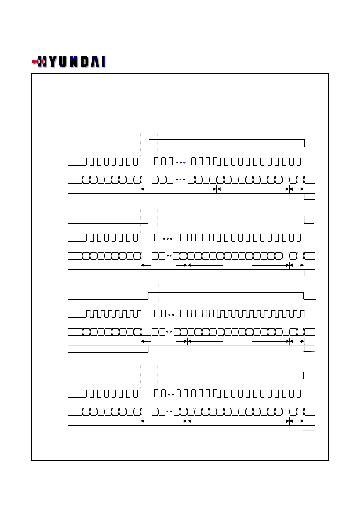
6. Serial I/O Data Format
1) Writing Mode
i )SCK is stopped at the low level
CE
SCK
HL15604
SI
SO
CE
SCK
SI
SO
CE
SCK
SI
SO
A0 A1 A2 A3 A4 A5 A6 A7
A0 A1 A2 A3 A4 A5 A6 A7
A0 A1 A2 A3 A4 A5 A6 A7
0 1 0 0 0 0 1 0 D1 D2 D3XX
Display data
0 1 0 0 0 0 1 0 D45 D46 XX
Display data
0 1 0 0 0 0 1 0 D85 D86XX
Display data
D41
D42 D43 D44 0 0 S0 S1 K0 K1 P0 P1 SC DR 0 0
Control data DD
D83
D84 0 0 0 0 0 0 0 0 0 0 0 0 0 1
0 0
D123
D124
0 0 0 0 0 0 0 0 0 0 0 0 1 0
0
Fixed data DD
0
Fixed data DD
CE
SCK
SI
SO
A0 A1 A2 A3 A4 A5 A6 A7
D163
0 1 0 0 0 0 1 0 D125 D126XX
Display data
D164
0 0 0 0 0 0 0 0 0 0 0 0 1 1
0
0
Fixed data DD
7
Page 8
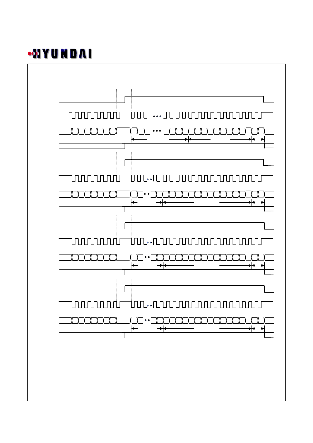
ii )SCK is stopped at the high level
CE
SCK
HL15604
SI
SO
CE
SCK
SI
SO
CE
SCK
SI
SO
1 0 0 0 0 1 0 0 D2 D3XX
A0 A1 A2 A3 A4 A5 A6 A7
1 0 0 0 0 1 0 0 D46XX
A0 A1 A2 A3 A4 A5 A6 A7
1 0 0 0 0 1 0 0 D86XX
A0 A1 A2 A3 A4 A5 A6 A7
D1
D45
D85
Display data
Display data
D41
D42 D43 D44 0 0 S0 S1 K0 K1 P0 P1 SC DR 0 0
Display data
D83
D84 0 0 0 0 0 0 0 0 0 0 0 0 0 1
0 0
Control data DD
Fixed data DD
D123
D124
0 0 0 0 0 0 0 0 0 0 0 0 1 0
0 0
Fixed data DD
CE
SCK
SI
SO
D163
1 0 0 0 0 1 0 0 D126XX
A0 A1 A2 A3 A4 A5 A6 A7
D125
Display data
D164
0 0 0 0 0 0 0 0 0 0 0 0 1 1
0 0
Fixed data DD
A7~A0 : 42H address
D164~D1 : Data of LCD display registers
S0, S1 : Sleep control data
K0, K1 : Key scan output / Segment output selection data
P0, P1 : Segment output / general-purpose output port selection data
SC : Segment on / off control data
DR : 1/2 bias or 1/3 bias drive selection data
8
Page 9
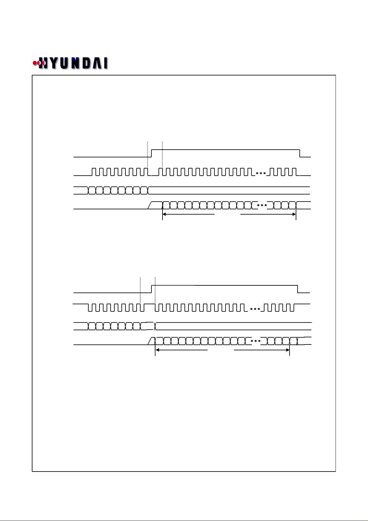
2) Reading Mode
i ) SCK is stopped at the low level
CE
SCK
HL15604
SI
SO
ii ) SCK is stopped at the high level
CE
SCK
SI
SO
01000011XX XX
A7A5A3A1 A6A4A2A0
K1 K2 K3 K4 K5 K6 K7 K8 K9 K11
0
1000011XX XX
A7A5A3A1 A6A4A2A0
XX
K1 K2 K3 K4 K5 K6 K7 K8 K9 K11
K29
K10
Output data
K30
XXK12 SAXX
X : don’ t care
K30
XX
X : don’ t care
Output data
K10
K12 SA
K29
A7 ~ A0 : 43H address
K30 ~ K1 : Key data
SA : Sleep acknowledge
9
Page 10
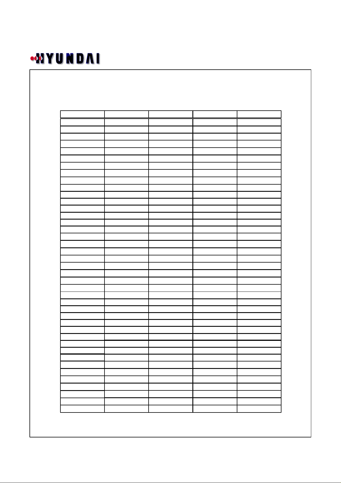
7. Registers
1) Display Registers
HL15604
Output Pin COM1 COM2 COM3
SEG1 D1 D2 D3
SEG2 D5 D6 D7
SEG3 D9 D10 D11
SEG4 D13 D14 D15
SEG5 D17 D18 D19
SEG6 D21 D22 D23
SEG7 D25 D26 D27
SEG8 D29 D30 D31
SEG9 D33 D34 D35
SEG10 D37 D38 D39
SEG11 D41 D42 D43
SEG12 D45 D46 D47
SEG13 D49 D50 D51
SEG14 D53 D54 D55
SEG15 D57 D58 D59
SEG16 D61 D62 D63
SEG17 D65 D66 D67
SEG18 D69 D70 D71
SEG19 D73 D74 D75
SEG20 D77 D78 D79
SEG21 D81 D82 D83
SEG22 D85 D86 D87
SEG23 D89 D90 D91
SEG24 D93 D94 D95
SEG25 D97 D98 D99
SEG26 D101 D102 D103
SEG27 D105 D106 D107
SEG28 D109 D110 D111
SEG29 D113 D114 D115
SEG30 D117 D118 D119
SEG31 D121 D122 D123
SEG32
SEG33
SEG34
SEG35
SEG36
SEG37
SEG39
D125 D126 D127
D129 D130 D131
D133 D134 D135
D137 D138 D139
D141 D142 D143
D145 D146 D147
D149 D150 D151SEG38
D153 D154 D155
D157 D158 D159SEG40
D161 D162 D163SEG41
COM4
D4
D8
D12
D16
D20
D24
D28
D32
D36
D40
D44
D48
D52
D56
D60
D64
D68
D72
D76
D80
D84
D88
D92
D96
D100
D104
D108
D112
D116
D120
D124
D128
D132
D136
D140
D144
D148
D152
D156
D160
D164
10
Page 11
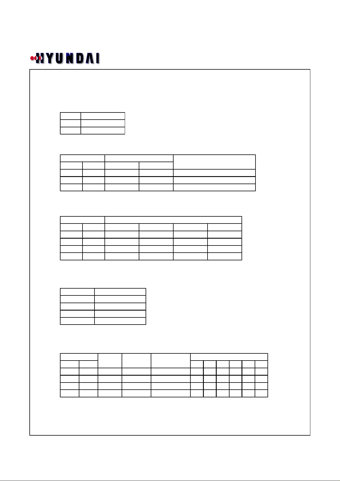
2) Control Registers
Bias Selection Register
HL15604
DR
Bias Selection
0
1 1/2 Bias
1/3 Bias
Key Scan / Segment output Selection Register
Control Data
K0 K1
0 0
0 1
1 X
Output Pin Status
KS1/SEG40 KS2/SEG41
KS1 KS2
SEG40 KS2
SEG40 SEG41
Maximum number of Input Pins
Port Mode Register
Control Data
P0 P1
0 0
0 1
1 0
1 1
SEG1/ P1 SEG2/ P2
SEG1 SEG2
P1 P2
P1 P2
P1 P2 P3 P4
Output Pin Status
SEG3/ P3 SEG4/ P4
SEG3 SEG4
SEG3 SEG4
P3 SEG4
30
25
20
Port Data Register
Output Pin
SEG1 / P1
SEG2 / P2
SEG3 / P3
SEG4 / P4
Port Data Register
D1
D5
D9
D13
Sleep Mode Control Register
Control Data
S0 S1
0 0
0 1
1 0
1 1
Mode
Normal
Sleep
Sleep
Sleep
OSC
Oscillator
Operating
Stopped
Stopped
Stopped
SEG / COMMON
Output
Operating
L
L
L
11
Output Pin Status
KS1 KS2
H H
L L
L L
H H
KS3 KS4
H H
L L
L L
H H
KS5 KS6
H H
L H
H H
H H
Page 12
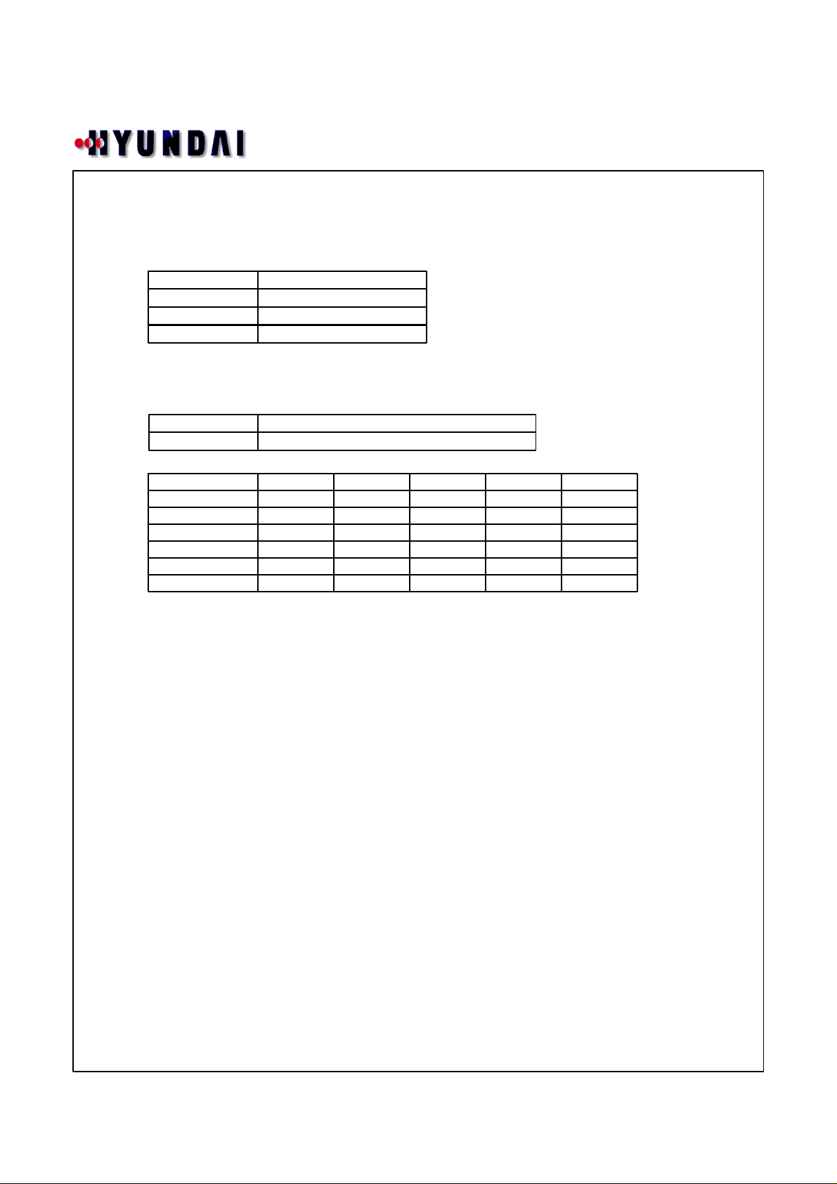
Display On/Off Control Register
HL15604
Control Data
SC
0
1
Display Status
SEG1 ~ SEG41
On
Off
Key Scan Data & Sleep Acknowledge Read
ADDRESS Read Data
K1 ~ K30, SA43H
KIN1 KIN2 KIN3 KIN4 KIN5
KS1 / SEG40
KS2 / SEG41
KS3
KS4
KS5
KS6
K1 K2 K3 K4 K5
K6 K7 K8 K9 K10
K11 K12 K13 K14 K15
K16 K17 K18 K19 K20
K21 K22 K23 K24 K25
K26 K27 K28 K29 K30
12
Page 13
HL15604
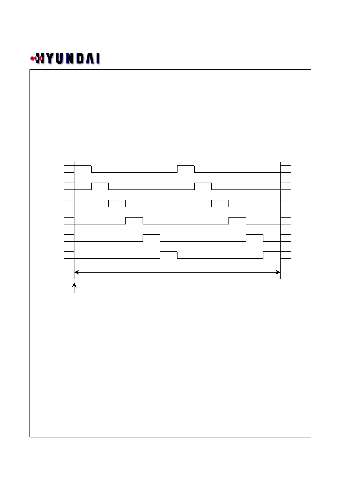
8. Key Scan Function
1) Key Scan Timing
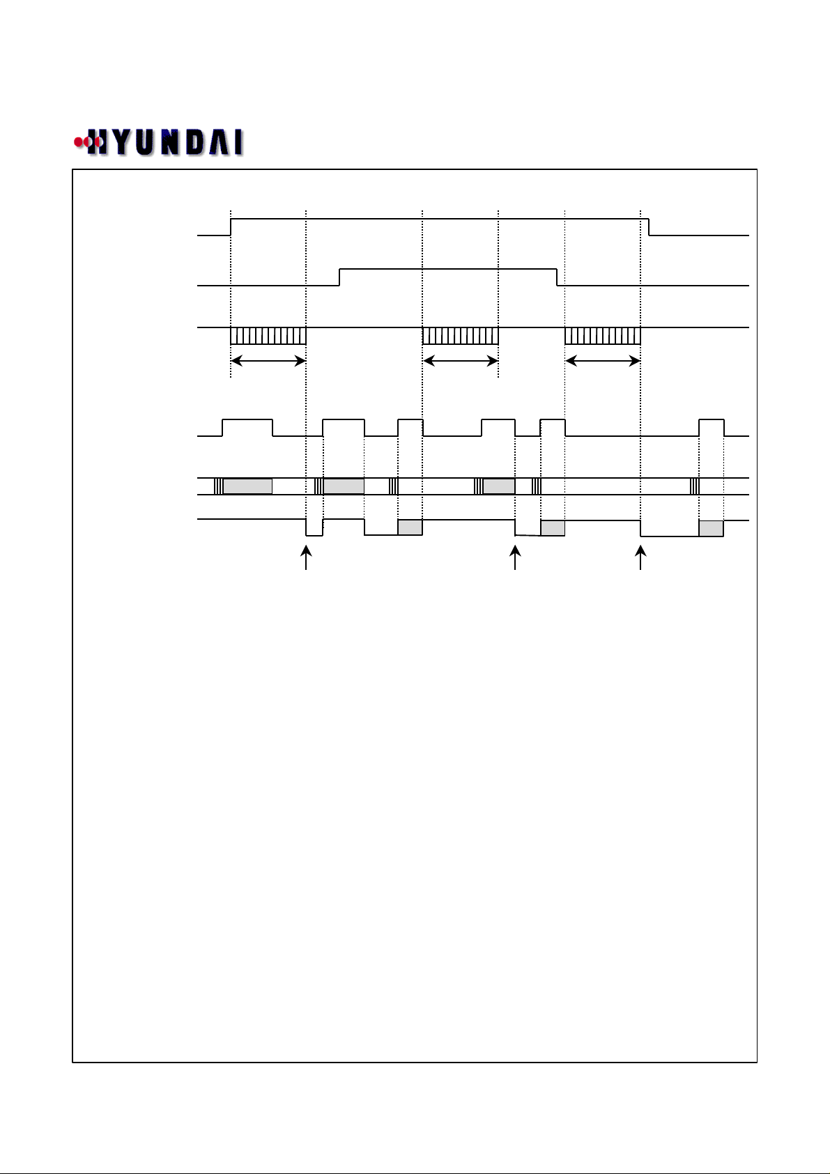
The key scan period is 384T. The HL14104 scans the key twice and determines
that a key has been pressed when the key data agrees. It outputs a key data read
request 800T after starting a key scan. If the key data does not agree and a key
was pressed at that point, it scans the key again.Thus the HL14104 cannot detect
a key press shorter than 800T.
KS1
KS2
KS3
KS4
KS5
KS6
*)
1
*)
*)
*)
*)
*) *)
2
3
4
5
1
2
3
4
5
6
768T
Key on
*) In sleep mode the high / low state of these pins is determined by the S0,S1 bits in the control data.
Key scan output signals are not output from pins that are set low.
2) In normal mode
*)
*)
*)
*)
*)
6
• The pins KS1 to KS6 are set high.
• When a key is pressed a key scan is started and the keys are scanned until all
keys are released. Multiple key presses are recognized by determining whether
multiple key data bits are set.
• If a key is pressed for longer than 800T ( where T=1/fosc ) the HL14104
outputs a key data read request (a low level on SO pin) to the controller. The
controller acknowledges this request and reads the key data. However, if CE
is high during a serial data transfer, SO will be set high.
• After the controller reads the key data, the key data read requests is cleared (
SO pin is set high ) and the HL14104 performs another key scan. Also note
that SO pin, being an open-drain output, requires a pull-up resistor.
13
Page 14
Key input 1
Key input 2
Key Scan
CE
SI
SO
Write
address
800T 800T 800T
Write
address
Read
address
Write
address
Read
address
HL15604
Read
address
Key data read Key data read Key data read
Key data read request
Key data read request Key data read request
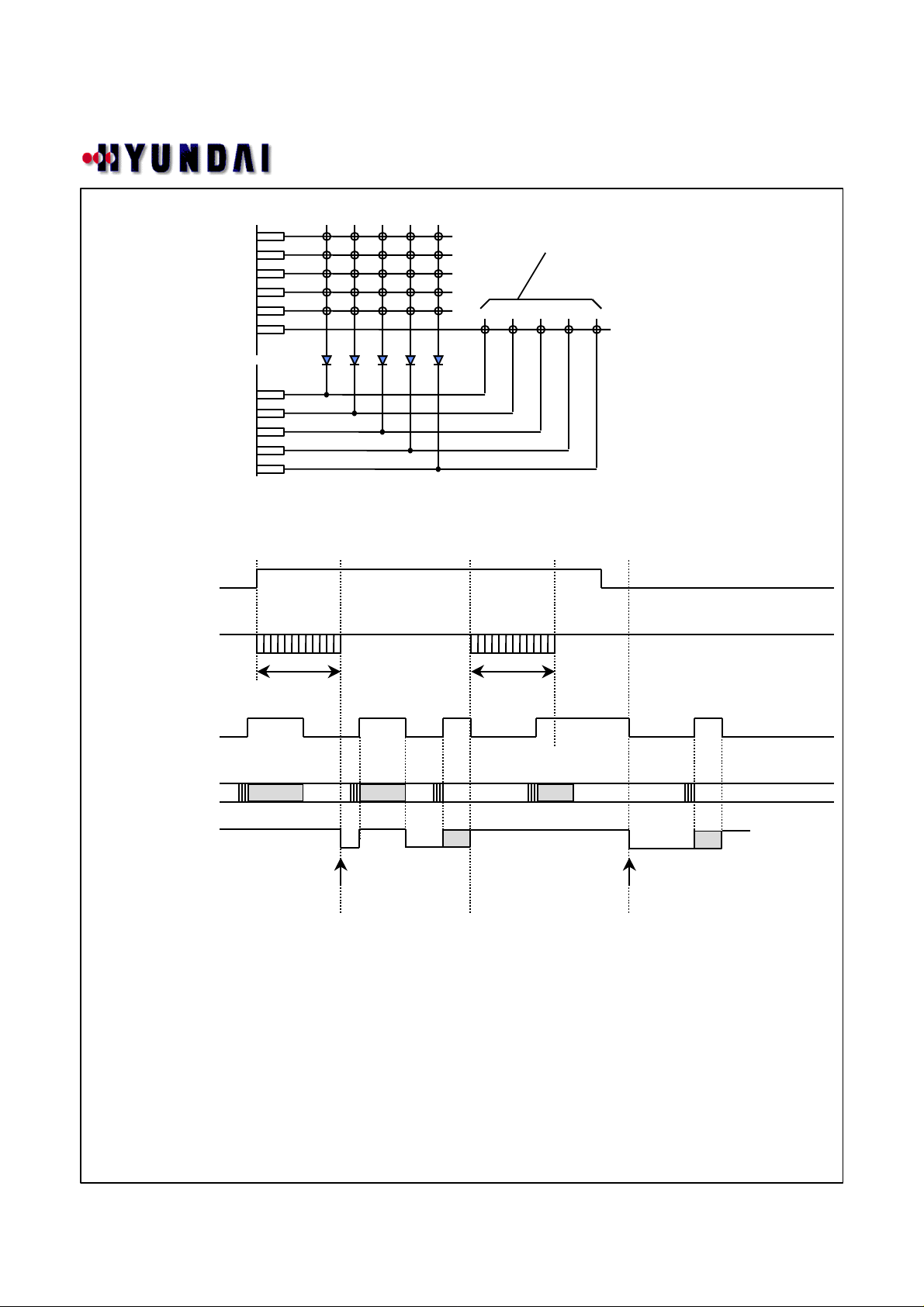
3) In sleep mode
• The pins KS1 to KS6 are set to high or low by the S0 and S1 bits in the
sleep mode control register.
• If a key on one of the lines corresponding to a KS1 to KS6 pin which is set
high is pressed, the oscillator on the OSC pin is started and a key scan is
performed. Keys are scanned until all keys are released. Multiple key pre sses are recognized by determining whether multiple key data bits are set.
• If a key is pressed for longer than 800T ( where T=1/fosc ) the HL14104
outputs a key data read request (a low level on SO) to the controller. The
controller acknowledges this request and reads the key data. However, if
CE is high during a serial data transfer, SO will be set high.
• After the controller reads the key data, the key data read request is cleared
( SO is set high ) and the HL14104 performs another key scan. However
this does not clear sleep mode. Also note that SO, being an open-drain
output, requires a pull-up resistor ( between 1 and 10 K).
• Sleep mode key scan example
Example : S0 = 0, S1 = 1 ( sleep with only KS6 high )
14
Page 15
HL15604
“L” KS1
“L” KS2
“L” KS3
When any one of these keys is pressed, the
oscillator on the OSC pin is started and the keys
are scanned.
“L” KS4
“L” KS5
“H” KS6
*)
KIN1
KIN2
KIN3
KIN4
KIN5
*) These diodes are required to reliable recognize multiple key presses on the KS6 line when sleep mode state with only
KS6 high, as in the above example. That is, these diodes prevent incorrect operation due to sneak currents in the KS6
key scan output signal when keys on the KS1 to KS5 lines are pressed at the same time.
Key input
(KS6 line)
Key Scan
800T 800T
CE
Write
address
Write
address
Read
address
Write
address
Read
address
SI
SO
Key data read Key data read
Key data read request
Key data read request
Multiple Key Presses
Although the HL14104 is capable of key scanning without inserting diodes for
dual key presses, triple key presses on the KIN1 to KIN5 input pin lines, or multiple key presses on the KS1 to KS6 output pin lines, multiple presses other than
these cases may result in keys that were not pressed recognized as having been
pressed. Therefore, a diode must be inserted in series with each key. Application
that do not recognize multiple key presses of threes or keys should check the key
data for three or more 1 bits and ignore such data.
15
Page 16
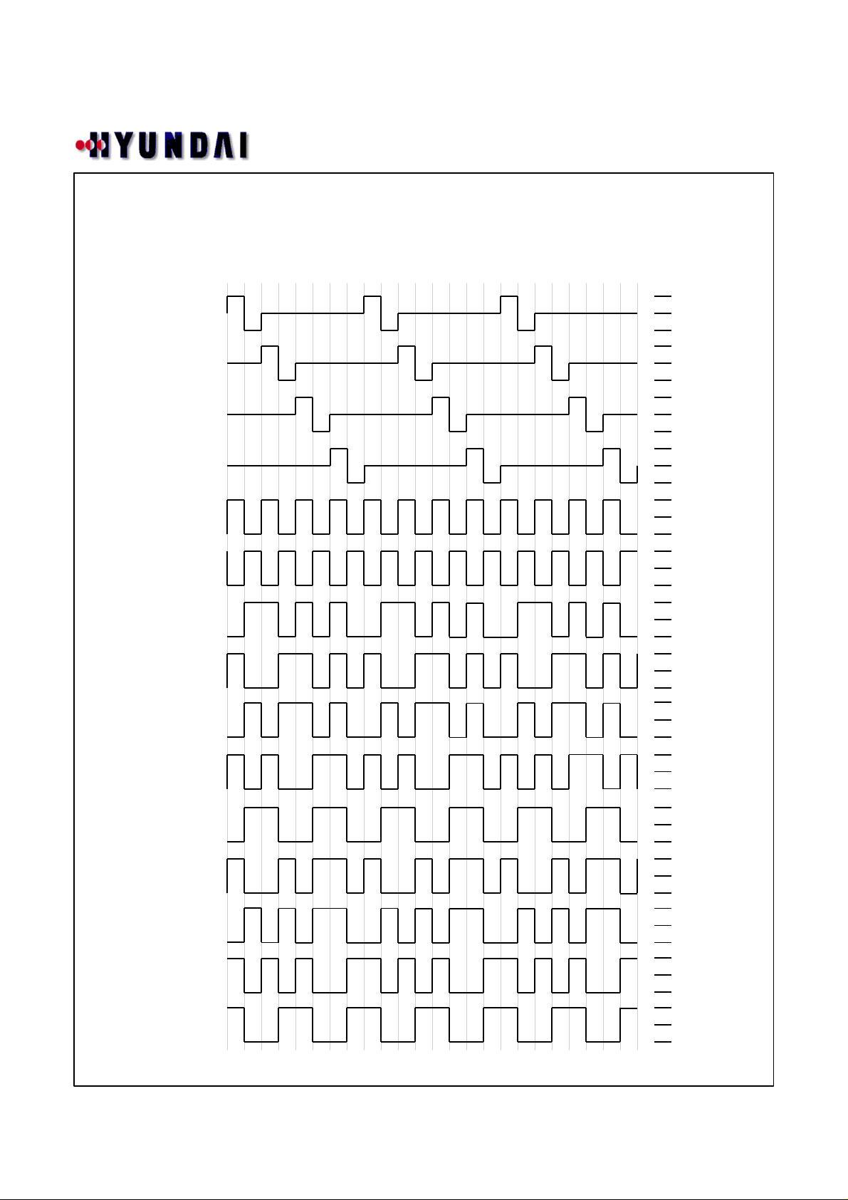
9. LCD Display Function
1) 1/4 Duty 1/2 Bias Waveforms
COM1
COM2
COM3
COM4
SEG1 ~ SEG41
“Off” at COM1
~ COM4
SEG1 ~ SEG41
“On” at COM1
~ COM4
SEG1 ~ SEG41
“On” at COM1
only
SEG1 ~ SEG41
“On” at COM2
only
SEG1 ~ SEG41
“On” at COM1
and COM2
SEG1 ~ SEG41
“On” at COM3
only
SEG1 ~ SEG41
“On” at COM1
and COM3
SEG1 ~ SEG41
“On” at COM2
and COM3
SEG1 ~ SEG41
“On” at COM1,
COM2 and COM3
SEG1 ~ SEG41
“On” at COM4
only
SEG1 ~ SEG41
“On” at COM2
and COM4
HL15604
VDD
VCL1,VCL2
0
VDD
VCL1,VCL2
0
VDD
VCL1,VCL2
0
VDD
VCL1,VCL2
0
VDD
VCL1,VCL2
0
VDD
VCL1,VCL2
0
VDD
VCL1,VCL2
0
VDD
VCL1,VCL2
0
VDD
VCL1,VCL2
0
VDD
VCL1,VCL2
0
VDD
VCL1,VCL2
0
VDD
VCL1,VCL2
0
VDD
VCL1,VCL2
0
VDD
VCL1,VCL2
0
VDD
VCL1,VCL2
0
16
Page 17
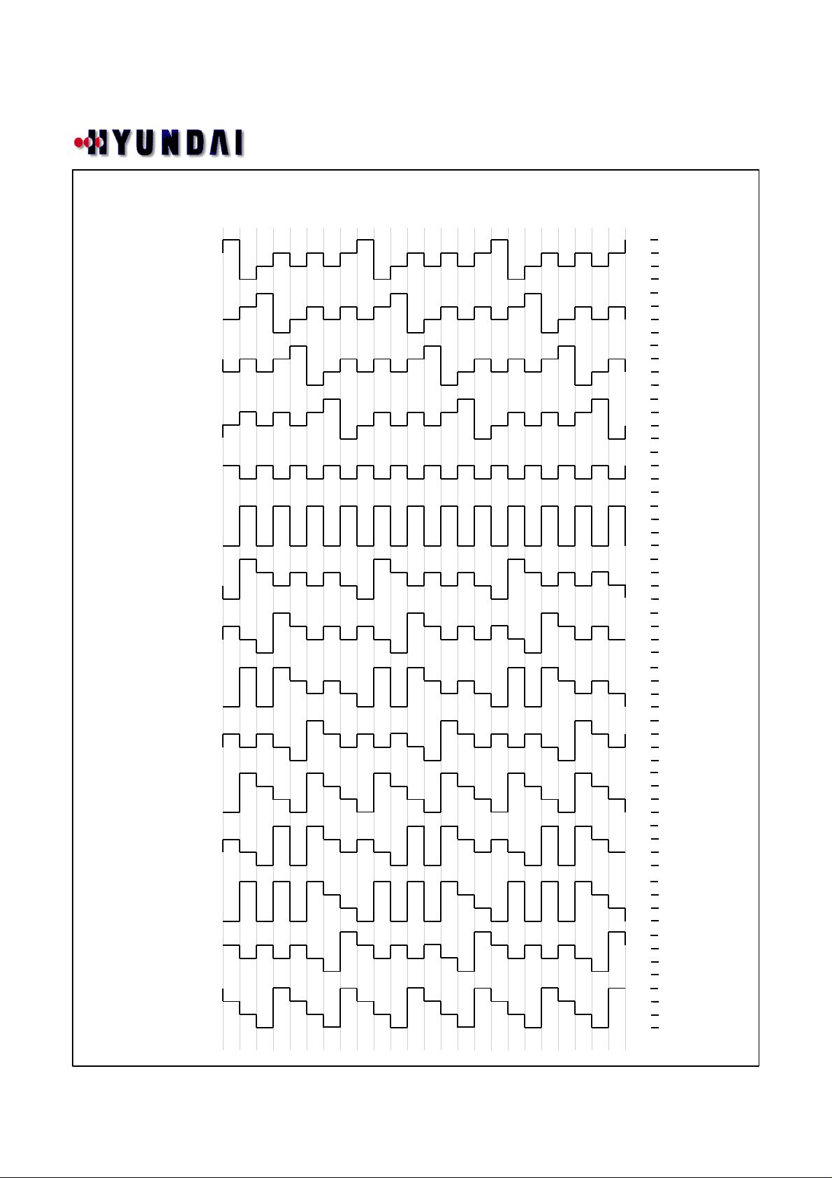
2) 1/4 Duty 1/3 Bias Waveforms
COM1
COM2
COM3
COM4
SEG1 ~ SEG41
“Off” at COM1
~ COM4
SEG1 ~ SEG41
“On” at COM1
~ COM4
SEG1 ~ SEG41
“On” at COM1
only
SEG1 ~ SEG41
“On” at COM2
only
SEG1 ~ SEG41
“On” at COM1
and COM2
SEG1 ~ SEG41
“On” at COM3
only
SEG1 ~ SEG41
“On” at COM1
and COM3
SEG1 ~ SEG41
“On” at COM2
and COM3
SEG1 ~ SEG41
“On” at COM1,
COM2 and COM3
SEG1 ~ SEG41
“On” at COM4
only
SEG1 ~ SEG41
“On” at COM2
and COM4
HL15604
VDD
VCL1
VCL2
0
VDD
VCL1
VCL2
0
VDD
VCL1
VCL2
0
VDD
VCL1
VCL2
0
VDD
VCL1
VCL2
0
VDD
VCL1
VCL2
0
VDD
VCL1
VCL2
0
VDD
VCL1
VCL2
0
VDD
VCL1
VCL2
0
VDD
VCL1
VCL2
0
VDD
VCL1
VCL2
0
VDD
VCL1
VCL2
0
VDD
VCL1
VCL2
0
VDD
VCL1
VCL2
0
VDD
VCL1
VCL2
0
17
Page 18
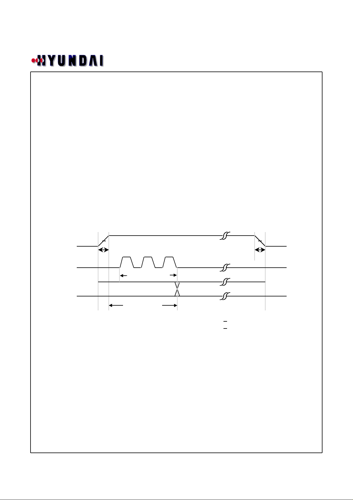
10. Power On Reset
1) Supply Voltage Detection ( SVD )
The SVD generates an output signal and results the system when power is
first applied and when the voltage drops. When the power supply voltage is
less than or equal to the power down detection voltage, which is 2.0V, typical.
To assure that this function operates reliably, a capacitor must be added to the
power supply voltage Vdd rise time when power is first applied and the power
supply voltage Vdd fall time when the voltage drops are both at least 1ms.
2) System Reset
If at least 1ms is assured as the supply voltage Vdd rise time when power is
applied, a system reset will be applied by the SVD output signal when the supply
voltage is brought up. If at least 1ms is assured as the supply voltage Vdd fall
time when power drops, a system reset will be applied in the same manner by
the SVD output signal when the supply voltage is lowered.
HL15604
VDD
CE
Internal data
SVD
t1 t2
Display and control data transfer
Undefined
System reset period
Power supply voltage Vdd rise time : t1 > 1ms
Power supply voltage Vdd fall time : t2 > 1ms
Defined
SVD
3) Internal block states during the reset period
• Clock generator
Reset is applied and the base clock is stopped and OSC pin state is low.
• Common , segment drive and display data
Reset is applied and the display is turned off but display data is not cleared.
• Key scan
Reset is applied and all the key data is set to low.
18
Page 19

4) Output pin states during the reset period
• SEG1/P1 to SEG4/P4 : Low *)
• SEG5 to SEG39 : Low
• COM1 to COM4 : Low
• KS1/SEG40, KS2/SEG41 : Low *)
• KS3 to KS5 : X **)
• KS6 : High
• SO : High ***)
*) These output pins are forcibly set to the segment output function and held low.
**) When power is first applied, these output pins are undefined until the S0 and S1 control
data bits have been transferred.
***) Since this output pin is an open-drain output, a pull-up resistor of between 1 and 10§Ú is
required. This pin remains high during the reset period even if a key data read operation
is performed.
HL15604
11. Power Down Mode
Sleep mode is set up by setting S0 or S1 in the control data to 1. The segment
outputs will all go low and the common outputs will also go low, and the oscillator
on the OSC pin will stop ( it will be started by a key press). This reduces power
dissipation. This mode is cleared by sending control data with both S0 and S1 set
to 0. Note that the SEG1/P1 to SEG4/P4 outputs can be used as general purpose
output ports according to the state of the P0 and P1 control data bits, even in
sleep mode.
19
Page 20
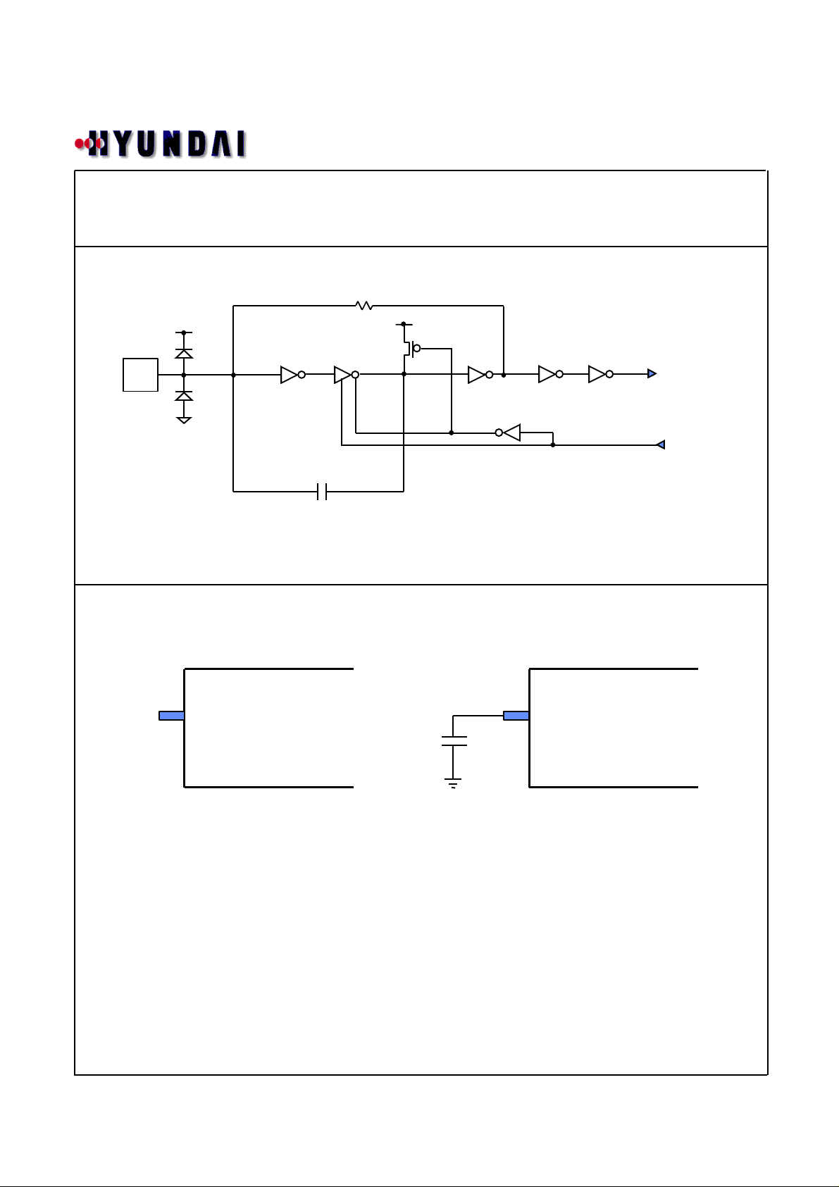
12. Oscillator Port
OSC Pin Diagram
OSC
HL15604
R
Internal clock
SLEEP
C
Oscillator circuit consists of internal R and C.
No Capacitor
OSC
Open
HL14104 has internal resistor and capacitor, so it can be oscillation without external capacitor.
If you want to adjust the clock period then you adjust it using external capacitor.
Using Capacitor
OSC
C
20
Page 21
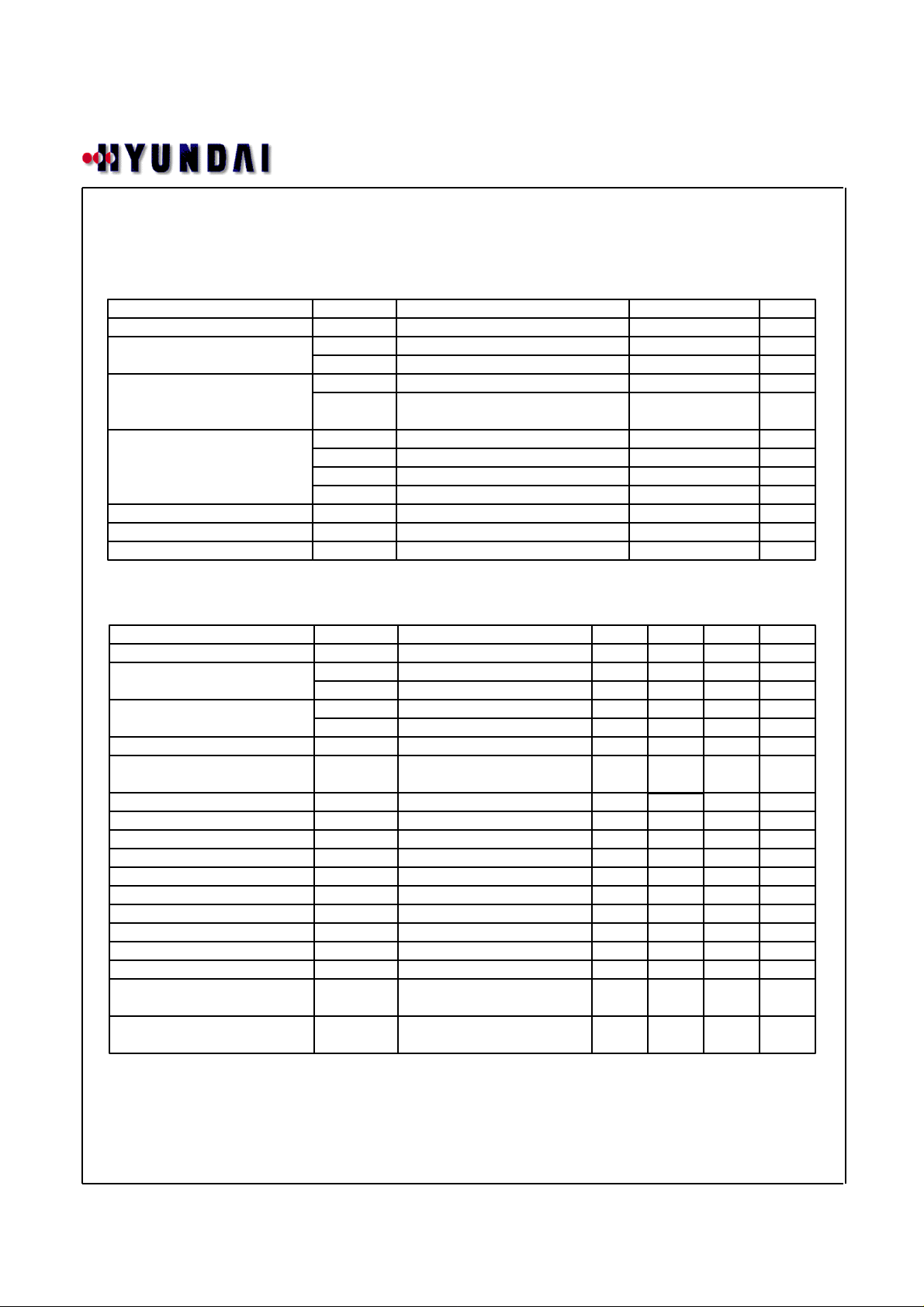
13. Electrical Characteristics
Absolute Maximum Rating at Ta=25¡É, Vss = 0V
HL15604
Parameter Symbol Condition
Maximum supply voltage VDD max VDD
Input voltage
Output voltage
Output current
Allowable power dissipation Pd max
Operating temperature Topr -40 to +85
Storage temperature Tstg -55 to +125
Vin1 CE,SCK,SI -0.3 to +7.0 V
Vin2 OSC,KIN1 to KIN5, TEST,VCL1,2 -0.3 to VDD+0.3 V
Vout1 SO -0.3 to +7.0 V
Vout2
Iout1 SEG1 to SEG41 300 uA
Iout2 COM1 to COM4 3 mA
Iout3 KS1 to KS6 1 mA
Iout4 P1 to P4 5 mA
OSC, SEG1 to SEG41, COM1 to
COM4, KS1 to KS6, P1 to P4
Ta = 85¡É
Rating unit
-0.3 to +7.0 V
-0.3 to VDD+0.3 V
200 mW
Recommend operating ranges at Ta= -40¡É to +85¡É, Vss = 0V
Parameter Symbol Condition
Supply voltage VDD
Input voltage
Input high level voltage
Recommended external
capacitance
Guaranteed oscillation range KHz
Data setup time ns
Data hold time ns
CE wait time
CE setup time
CE hold time
High level clock pulse width
Low level clock pulse width
Rise time
Fall time
SO output delay time
SO rise time
VCL1 V
VCL2 V
VIH1 V
VIH2
VILInput low level voltage
f
OSC
tds
tdh
tcp
tcs
tch
t0H
toL
tr
tf
tdc
tdr
VDD
VCL1
VCL2
CE,SCK,SI
KIN1 to KIN5
CE,SCK,SI,KIN1 to KIN5
OSC
OSC
SCK,SI
SCK,SI
CE,SCK
CE,SCK
CE,SCK
SCK
SCK
CE,SCK,SI
CE,SCK,SI
SO,RPU = 4.7kΩ,
CL = 10pF*
SO,RPU = 4.7kΩ,
CL = 10pF*
min
4.5
0.8VDD
0.6VDD
160
160
160
160
160
160
160
typ
2/3VDD
1/3VDD
0
0
30
55
max
6.0
VDD
VDD
6.0
VDD
0.2VDD
100
76
¡É
¡É
unit
V
V
V
pFCOSC
ns
ns
ns
ns
ns
ns160
ns160
µs1.5
µs1.5
Note : *. Since SO is an open-drain output, these values depend on the resistance of the pull-up resistor RPU and
load capacitance CL .
21
Page 22
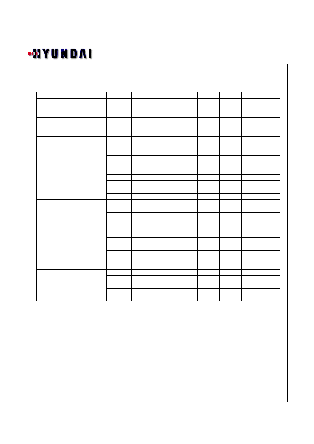
Electrical Characteristics for the Allowable Operating Ranges
HL15604
Parameter Symbol Condition
Hysteresis VH
Supply voltage detection SVD V
IIH µAInput high level current
Input low level current
Pull-down resistance
Output off leakage current
Output high level voltage
Output low level voltage
Output middle level voltage*
Oscillator frequency f
Current drain
IIL µA
VIFInput floating voltage
RPD
IOFFH
VOH1
VOH2
VOH3
VOH4
VOL1
VOL2
VOL3
VOL4
VOL5
VMID1
VMID2
VMID3
VMID4
VMID5
OSC
IDD1 µA100Sleep mode
IDD2 µA700
IDD3 µA600
CE,SCK,SI
CE,SCK,SI : V1 = 6.0V
CE,SCK,SI : V1 = 0V
KIN1 to KIN5
KIN1 to KIN5 : VDD = 5.0V
SO : VO = 6.0V
KS1 to KS6 : I0 = -500µA
P1 to P4 : I0 = -1mA
SEG1 to SEG41 : I0 = -20µA
COM1 to COM4 : I0= -100µA
KS1 to KS6 : I0 = 25µA
P1 to P4 : I0 = 1mA
SEG1 to SEG41 : I0 = 20µA
COM1 to COM4 : I0 = 100µA
SO : I0 = 1 mA
COM1 to COM4 : 1/2 bias,
Io = ¡¾100µA
SEG1 to SEG41 : 1/3 bias,
Io = ¡¾20µA
SEG1 to SEG41 : 1/3 bias,
Io = ¡¾20µA
COM1 to COM4 : 1/3 bias,
Io = ¡¾100µA
COM1 to COM4 : 1/3 bias,
Io = ¡¾100µA
VDD = 6.0V, output open,
1/2 bias,f
VDD = 6.0V, output open,
1/3 bias,f
= 38 KHz
OSC
= 38 KHz
OSC
min
1.5
-5.0
50
VDD -1.2
VDD -1.0
VDD -1.0
VDD -1.0
0.2
1/2 VDD
-1.0
2/3VDD
-1.0
1/3VDD
-1.0
2/3VDD
-1.0
1/3VDD
-1.0
typ
O.1VDD
2.0
100
VDD -0.5
0.5
0.1
55
350
300
max
0.05VDD
250
1/2VDD
+1.0
2/3VDD
+1.0
1/3VDD
+1.0
2/3VDD
+1.0
1/3VDD
+1.0
3.0
5.0
6.0
1.5
1.0
1.0
unit
kΩ
µA
KHz7045OSC : C = 0
V
V
V
V
V
V
V
V
V
V1.0
V0.5
V
V
V
V
V
Note : *. Excluding the bias voltage generation divider resistor built into VCL1 and VCL2
22
Page 23
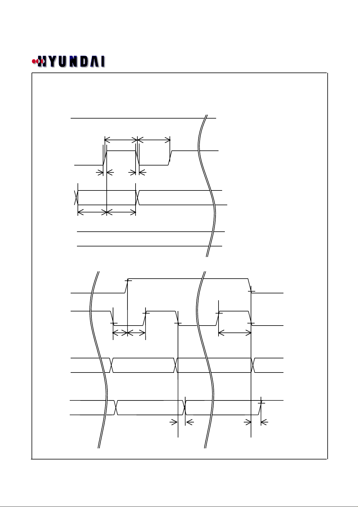
Timing diagram of SIO
CE
HL15604
SCK
SI
SO
CE
t0H
tr tf
tds tdh
VIH1
t0L
VIL
SCK
SI
SO
tcp tcs
tdc
23
tch
tdr
Page 24
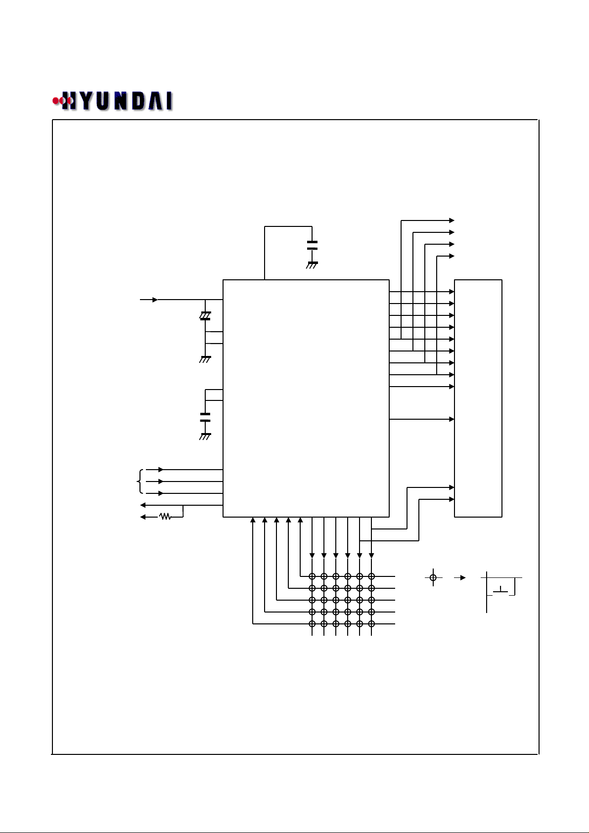
14. Application
LCD panel (up to 164 segments)
1/2 bias ( for use with normal panels )
HL15604
(p 1)
(general-purpose
output ports)
(p 2)
Used with the
(p 3)
backlight controller
(p 4)
or other circuit.
+5V
C ≥ 0.047uF
From the controller
To the controller
To the controller
power supply
*2)
*1)
OSC
VDD
VSS
TEST
VCL1
VCL2
C
CE
SCK
K
K
K
K
K
K
SI
SO
I
I
I
N
5
I
N
N
N
4
3
2
K
I
S
S
N
6
5
1
COM1
COM2
COM3
COM4
P1 / SEG1
P2 / SEG2
P3 / SEG3
P4 / SEG4
SEG5
SEG39
S
E
G
4
1
/
K
K
K
S
S
S
3
2
4
.
.
.
.
.
S
E
G
4
0
/
K
S
1
.
.
.
.
.
(SEG40)
(SEG41)
•
Key matrix
(up to 30 keys)
Note : *1). Add a capacitor to the power supply line so that the power supply voltage VDD rise time when power is
applied and the power supply voltage VDD fall time when power drops are both at least 1 ms, as the
HL14104 is reset by the SVD.
*2). The SO pin, being an open-drain output, requires a pull-up resistor, Select a resistance (between 1 to 10kΩ)
appropriate for the capacitance of the external wiring so that signal waveforms are not degraded.
24
•
¡Æ
¡Æ
Page 25
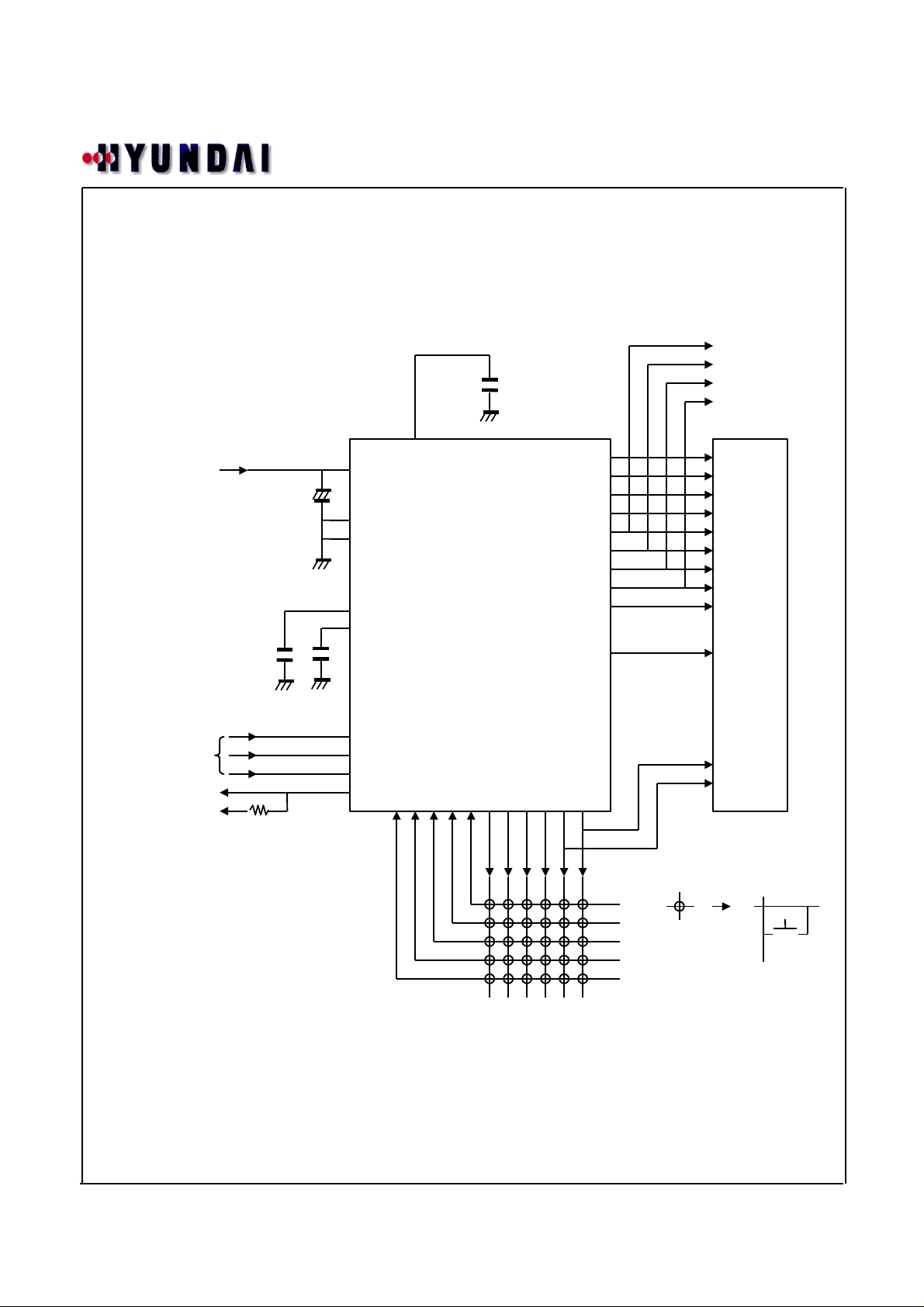
LCD panel (up to 164 segments)
1/3 bias ( for use with normal panels )
HL15604
(p 1)
(general-purpose
output ports)
(p 2)
Used with the
(p 3)
backlight controller
(p 4)
or other circuit.
+5V
C ≥ 0.047uF
From the controller
To the controller
To the controller
power supply
C C
*2)
*1)
VDD
VSS
TEST
VCL1
VCL2
CE
SCK
SI
SO
OSC
K
I
N
5
COM1
COM1
COM2
COM3
P1 / SEG1
P2 / SEG2
P3 / SEG3
P4 / SEG4
SEG5
.
.
.
.
.
SEG39
S
S
E
E
G
G
4
4
0
1
K
K
K
K
K
K
I
I
I
N
N
N
4
3
2
K
I
S
S
S
N
6
4
5
1
/
/
K
K
K
S
S
S
3
1
2
.
.
.
.
.
(SEG40)
(SEG41)
•
Key matrix
(up to 30 keys)
Note : *1). Add a capacitor to the power supply line so that the power supply voltage VDD rise time when power is
applied and the power supply voltage VDD fall time when power drops are both at least 1 ms, as the
HL14104 is reset by the SVD.
*2). The SO pin, being an open-drain output, requires a pull-up resistor, Select a resistance (between 1 to 10kΩ)
appropriate for the capacitance of the external wiring so that signal waveforms are not degraded.
25
•
¡Æ
¡Æ
Page 26
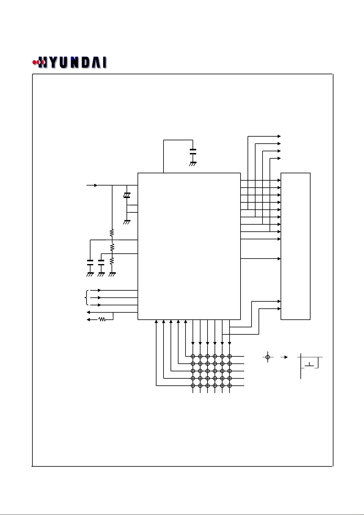
LCD panel (up to 164 segments)
1/3 bias ( for use with large panels )
HL15604
(p 1)
(general-purpose
output ports)
(p 2)
Used with the
(p 3)
backlight controller
(p 4)
or other circuit.
+5V
C ≥ 0.047uF
From the controller
To the controller
To the controller
power supply
OSC
VDD
*1)
VSS
TEST
R
•
R
C
C
•
R
*2)
VCL1
VCL2
CE
SCK
SI
SO
K
K
K
K
K
K
I
I
I
N
5
I
N
N
N
4
3
2
K
I
S
S
N
6
5
1
COM1
COM2
COM3
COM4
P1 / SEG1
P2 / SEG2
P3 / SEG3
P4 / SEG4
SEG5
SEG39
S
E
G
4
1
/
K
K
K
S
S
S
4
3
2
.
.
.
.
.
S
E
G
4
0
/
K
S
1
.
.
.
.
.
(SEG40)
(SEG41)
•
Key matrix
(up to 30 keys)
Note : *1). Add a capacitor to the power supply line so that the power supply voltage VDD rise time when power is
applied and the power supply voltage VDD fall time when power drops are both at least 1 ms, as the
HL14104 is reset by the SVD.
*2). The SO pin, being an open-drain output, requires a pull-up resistor, Select a resistance (between 1 to 10kΩ)
appropriate for the capacitance of the external wiring so that signal waveforms are not degraded.
26
•
¡Æ
¡Æ
 Loading...