

Page 1

HI-SINCERITY
MICROELECTRONICS CORP.
Spec. No. : HE6031
Issued Date : 1998.02.01
Revised Date : 2001.09.14
Page No. : 1/3
HJ117
PNP EPITAXIAL PLANAR TRANSISTOR
Description
The HJ117 is designed for use in general purpose amplifier and low-speed
switching applications.
Absolute Maximum Ratings (Ta=25°C)
• Maximum Temperatures
Storage Temperature .......................................................................................................... -55 ~ +150 °C
Junction Temperature .................................................................................................. +150 °C Maximum
• Maximum Power Dissipation
Total Power Dissipation (Tc=25°C) ................................................................................................... 20 W
• Maximum Voltages and Currents
BVCBO Collector to Base Voltage.................................................................................................. -100 V
BVCEO Collector to Emitter Voltage............................................................................................... -100 V
BVEBO Emitter to Base Voltage......................................................................................................... -5 V
IC Collector Current (Continue) .......................................................................................................... -4 A
IC Collector Current (Peak) ................................................................................................................ -6 A
Characteristics (Ta=25°C)
Symbol Min. Typ. Max. Unit Test Conditions
BVCBO -100 - - V IC=-1mA
BVCEO -100 - - V IC=-30mA
ICBO - - -1 mA VCB=-100V
ICEO - - -2 mA VCE=-50V
IEBO - - -2 mA VEB=-5V
*VCE(sat) - - -2.5 V IC=-2A, IB=-8mA
*VBE(on) - - -2.8 V IC=-2A, VCE=-4V
*hFE1 1 - - K IC=-1A, VCE=-4V
*hFE2 500 - - IC=-2A, VCE=-4V
Cob - - 200 pF VCB=-10V, f=0.1MHz
*Pulse Test : Pulse Width ≤380us, Duty Cycle≤2%
Darlington Schematic
C
B
R2R1
E
HJ117 HSMC Product Specification
Page 2
HI-SINCERITY
V
MICROELECTRONICS CORP.
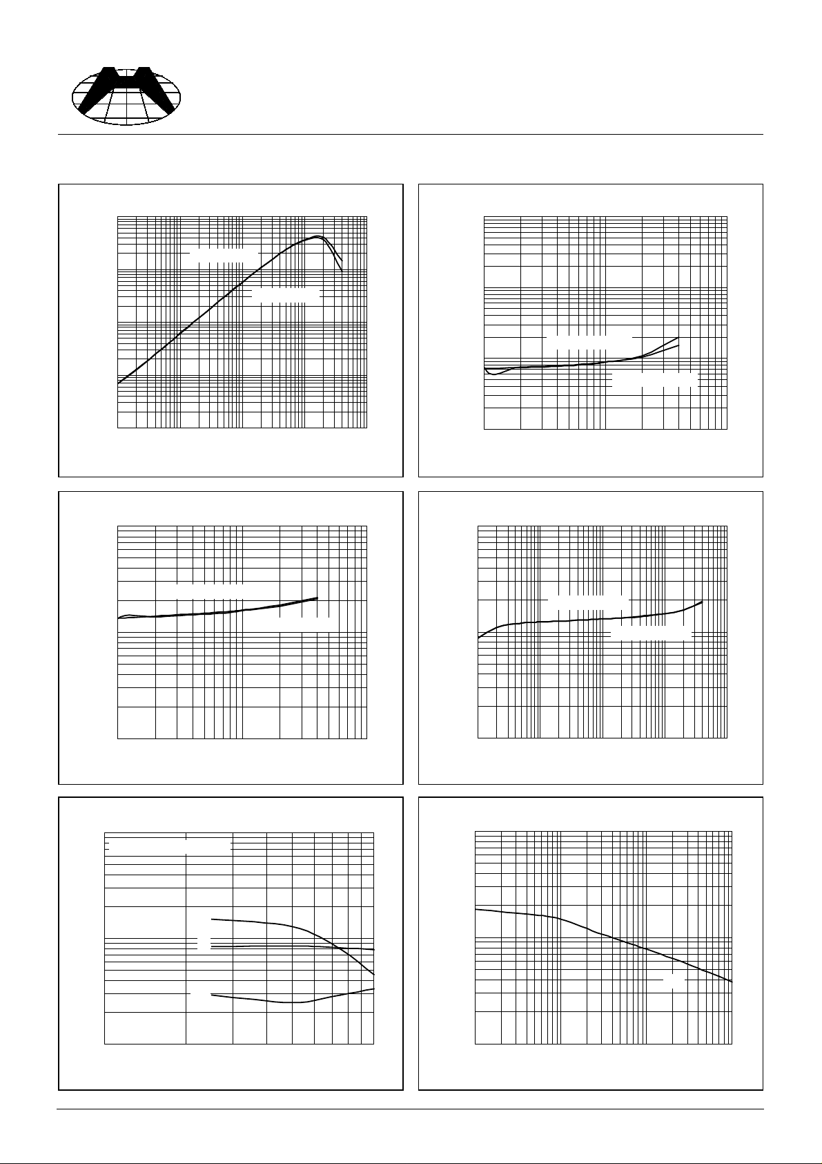
Characteristics Curve
Spec. No. : HE6031
Issued Date : 1998.02.01
Revised Date : 2001.09.14
Page No. : 2/3
10000
hFE @ VCE=3
1000
hFE @ VCE=4V
100
hFE
10
1
1 10 100 1000 10000
Collect or Cur rent-IC (mA)
Saturation Voltage & Collector Current
10000
Current Gain & Collector Current
1000
BE(sat)
V
@ IC=250I
B
BE(sat)
V
@ IC=100I
100000
10000
CE(sat)
V
@ IC=100I
1000
Satu r a tion Volta g e ( mV)
100
100 1000 10000
Col lector Cur rent-IC (mA)
B
CE(sat)
V
@ IC=250I
B
On V oltage & C o llector C urre nt
10000
BE(on)
V
@ VCE=3V
Satur ation Voltage & Collector Curre nt
B
1000
BE(on)
V
@ VCE=4V
On Voltage (mV)
Satu r a tion Volta g e ( mV)
100
100 1000 10000
Collect or Cur rent-IC (mA)
Switching Time & Collector Current
10
VCC=30V, IC=250IB1=-250I
1
Swit c hin g Time ( us)
0.1
110
B2
Tstg
Tf
Ton
Collecto r Cur rent (A)
100
1 10 100 1000 10000
1000
100
Capac itanc e ( p F )
10
Capacitance & Reverse-Biased Voltage
0.1 1 10 100
Collect or Cur rent-IC (mA)
Rev e r se-Biased Voltage (V)
Cob
HJ117 HSMC Product Specification
Page 3

HI-SINCERITY
MICROELECTRONICS CORP.
TO-252 Dimension
Spec. No. : HE6031
Issued Date : 1998.02.01
Revised Date : 2001.09.14
Page No. : 3/3
A
B
L
F
G
C
D
Marking:
Date Code
HJ
217
Ink Mark
Control Code
Style: Pin 1.Base 2.Collector 3.Emitter
3
H
E
K
2
I
1
J
3-Lead TO-252 Plastic Surface Mount Package
HSMC Package Code: J
*: Typical
DIM
Inches Millimeters Inches Millimeters
Min. Max. Min. Max.
DIM
Min. Max. Min. Max.
A 0.0177 0.0217 0.45 0.55 G 0.0866 0.1102 2.20 2.80
B 0.0650 0.0768 1.65 1.95 H - *0.0906 - *2.30
C 0.0354 0.0591 0.90 1.50 I - 0.0354 - 0.90
D 0.0177 0.0236 0.45 0.60 J - 0.0315 - 0.80
E 0.2520 0.2677 6.40 6.80 K 0.2047 0.2165 5.20 5.50
F 0.2125 0.2283 5.40 5.80 L 0.0551 0.0630 1.40 1.60
Notes: 1. Dimension and tolerance based on our Spec. dated May. 05,1996.
Material:
• Lead: 42 Alloy ; solder plating
• Mold Compound: Epoxy resin family, flammability solid burning class: UL94V-0
2. Controlling dimension: millimeters.
3. Maximum lead thickness includes lead finish thickness, and minimum lead thickness is the minimum thickness of base material.
4. If there is any question with packing specification or packing method, please contact your local HSMC sales office.
Important Notice:
• All rights are reserved. Reproduction in whole or in part is prohibited without the prior written approval of HSMC.
• HSMC reserves the right to make changes to its products without notice.
• HSMC semiconductor products are not warranted to be suitable for use in Life-Support Applications, or systems.
• HSMC assumes no liability for any consequence of customer product design, infringement of patents, or application assistance.
Head Office And Fac tory:
• Head Office (Hi-Sincerity Microelectronics Corp.): 10F.,No. 61, Sec. 2, Chung-Shan N. Rd. Taipei Taiwan R.O.C.
Tel: 886-2-25212056 Fax: 886-2-25632712, 25368454
• Factory 1: No. 38, Kuang Fu S. Rd., Fu-Kou Hsin-Chu Industrial Park Hsin-Chu Taiwan. R.O.C
Tel: 886-3-5983621~5 Fax: 886-3-5982931
HJ117 HSMC Product Specification
 Loading...