

Page 1
HI-SINCERITY
MICROELECTRONICS CORP.
Spec. No. : HE6732-A
Issued Date : 1998.07.01
Revised Date : 1999.08.01
Page No. : 1/5
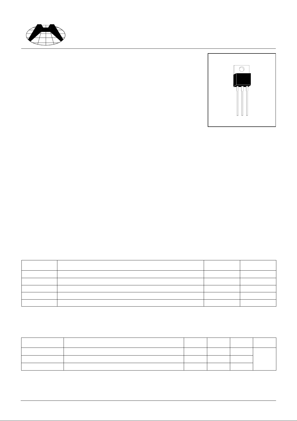
HIRF630
N - Channel MOSFETs
Description
Dynamic dv / dt Rating
Repetitive Avalanche Rated
•
Fast Switching
•
Ease of Paralleling
•
Simple Drive Requirements
•
This N - Channel MOSFETs provide the designer with the best combination of fast switching,
ruggedized device design, low on-resistance and cost-effectiveness.
Absolute Maximum Ratings
Maximum Temperatures
•
(Ta=25°C)
Storage Temperature............................................................................................ -55 ~ +150 °C
Junction Temperature..................................................................................... 150 °C Maximum
Maximum Power Dissipation
•
Total Power Dissipation (Tc=25°C) .................................................................................... 74 W
Maximum Voltages and Currents (Tc=25°C)
•
Drain To Source Breakdown Voltage................................................................................ 200 V
Gate To Source Voltage................................................................................................... ± 20 V
Continuous Source Current.................................................................................................. 9 A
Pulsed Drain Current.......................................................................................................... 36 A
Characteristics
(Ta=25°C)
Symbol Parameter Max. Units
ID Tc=25°C
Continuous Drain Current, VGS at 10V 9 A
EAS Single Pulse Aval anche Ener g y (1) 250 mJ
IAR Avalanche Current (2) 9 A
EAR Repetitive Avalanche Energy (2) 7.4 mJ
dv / dt Peak Diode Recovery dv / dt (3) 5 V / ns
Note : VDD=50V, starting TJ=25°C, L=4.6mH, RQ=25Ω, IAS=9A
Repetitive rating; width limited by max. Junction temperature. I
≤
9A, di/dt≤120A / us, V
SD
DD
≤
V
(BR)DSS
, T
≤
150°C
J
Thermal Resistance
Symbol Parameter Min. Typ. Max. Units
RθJC
RθCS
RθJA
Junction to Case - - 1.7
Case to Sink, Flat, Greased Surface - 0.5 Junction to Ambient - - 62
HSMC Product Specification
C/W
°
Page 2
HI-SINCERITY
MICROELECTRONICS CORP.
(Ta=25°C)
Characteristics
Symbol Min. Typ. Max. Unit Test Conditions
V(BR)DSS 200 - - V ID=100uA
VGS(th) 2 - 4 V VDS=4V, ID=250uA
IDSS - - 25 uA VDS=200V
IGSS - - 100 nA VGS=20V
IGSS - - -100 nA VGS=-20V
Qg - - 40 nC ID=10A
Qgs - - 8 nC VDS=200V
Qgd - - 10 nC VGS=10V
ton - 200 - nS VDD=100V
td(off) - 90 - nS ID=5A
tf - 6 0 - nS VGS=10V
VDS(on) - - 2 V ID=5.0A, VG = 10V
ID(on) 9 - - A VDS=10V, VGS=10V
RDS(on) - - 0.4
Ciss - 800 - pF VGS=0V
Coss - 240 - pF VDS=25V
Crss - 90 - pF f=1MHz
Ω
VGS=10V, ID = 5.4A
Spec. No. : HE6732-A
Issued Date : 1998.07.01
Revised Date : 1999.08.01
Page No. : 2/5
HSMC Product Specification
Page 3

HI-SINCERITY
MICROELECTRONICS CORP.
Characteristics Curve
Spec. No. : HE6732-A
Issued Date : 1998.07.01
Revised Date : 1999.08.01
Page No. : 3/5
14
12
10
VGS=10
8
6
4
Drain-Source Cur rent (A)
2
0
0246810
On-Region C ha racteri stic
8V
7V
6V
5V
4V
Drain-Source Voltage (V)
Drain Current Variation with Gate Voltage &
10
8
6
4
Drain-Source Cur rent (A)
2
0
02468
Temperature
TJ=125°C
TJ=25°C
Gate -Source Voltage (V)
On Resistance Variation with Temperature
2.5
ID= 3.5 A
2.3
GS
= 10 V
V
2.1
1.9
1.7
1.5
1.3
1.1
0.9
0.7
Norm alize d Drain-Source O n-Resistance
0.5
25 50 75 100 125 150
3000
2500
2000
1500
1000
Capac itance (pF)
500
0
0 1020304050
Junction Temperature (ºC)
Capacitance Characteristics
Crss
Drain-Source Voltage (V)
Ciss
Coss
Transconductance Variation with Drain Current
7
6
5
4
3
2
gFS,Transconductance (S)
1
0
0246810
& Temperature
Drain Curre nt (A)
TJ= 25°C
J
=125°C
T
Body Di ode Forward Voltage Variati on with
10
8
6
4
Reverse Drain Current (A)
2
0
0.2 0.4 0.6 0.8 1 1.2
Curren t & Temper ature
TJ= 25°C
Body Diode Forward Vol t ag e ( V)
HSMC Product Specification
Page 4

HI-SINCERITY
MICROELECTRONICS CORP.
Spec. No. : HE6732-A
Issued Date : 1998.07.01
Revised Date : 1999.08.01
Page No. : 4/5
Brea kdown Voltage Varia tion w ith Temperature
1.16
1.14
1.12
1.10
1.08
1.06
Voltage
1.04
1.02
Norm alize d Drain-Source Brea kdown
1.00
0.98
25 50 75 100 125 150
Junction Temperature (°C)
1.00
0.5
0.2
ID=250 uA
100
VGS=10 V
Single Pulse
C
=25°C
T
10
1
Drain-Source Current (A)
0
0.1 1 10 100 1000
Transient Thermal Response Curve
Max i mum Sa fe Operating Area
DS(on)
R
Line
Drain-Source Voltage (V)
100us
1ms
10ms
100ms
DC
0.10
Resistance
r(t) Normalized Effective Transient Thermal
0.01
0.1
0.05
0.02
0.01
Single Pulse
0.01 0.1 1 10 100 1000
Time (ms)
RθJC(t) = r(t) * RθJC(t)
RθJC =1.7 °C / W
P(pk)
t1
t2
TJ-TC=P* RθJC(t)
Duty Cycle,D=t1/t2
HSMC Product Specification
Page 5

HI-SINCERITY
MICROELECTRONICS CORP.
TO-220AB Dimension
A B
D
H
I
G
Spec. No. : HE6732-A
Issued Date : 1998.07.01
Revised Date : 1999.08.01
Page No. : 5/5
Marking :
E
M
C
K
HSMC Logo
Part Number
Date Code
Style : Pin 1.Gate 2.Drain 3.Source
Product Series
Rank
3
2
N
4
1
O
DIM
Min. Max. Min. Max.
DIM
P
3-Lead TO-220AB Plastic Package
HSMC Package Code : E
Inches Millimeters Inches Millimeters
Min. Max. Min. Max.
A 0.2197 0.2949 5.58 7.49 I - *0.1508 - *3.83
B 0.3299 0.3504 8.38 8.90 K 0.0295 0.0374 0.75 0.95
C 0.1732 0.185 4.40 4.70 M 0.0449 0.0551 1.14 1.40
D 0.0453 0.0547 1.15 1.39 N - *0.1000 - *2.54
E 0.0138 0.0236 0.35 0.60 O 0.5000 0.5618 12.70 14.27
G 0.3803 0.4047 9.66 10.28 P 0.5701 0.6248 14.48 15.87
H - *0.6398 - *16.25
Notes :
Material :
• Lead : 42 Alloy ; solder plating
• Mold Compound : Epoxy resin family, flammability solid burning class:UL94V-0
1.Dimension and tolerance based on our Spec. dated Sep. 07,1997.
2.Controlling dimension : millimeters.
3.Maximum lead thickness includes lead finish thickness, and minimum lead thickness is the minimum thickness of base material.
4.If there is any question with packing specification or packing method, pleas e contact your l ocal HSMC sal es office.
*:Typical
Important Notice:
• All rights are reserved. Reproduction in whole or in part is prohibited without the prior written approval of HSMC.
• HSMC reserves the right to make changes to its products without notice.
•
HSMC semiconductor products are not warranted to be suitable for use in Life-Support Applications, or systems.
• HSMC assumes no liability for any consequence of customer product design, infringem ent of pat ents, or applic ati on assistance.
Head Office And Factory :
•
Head Office
Tel : 886-2-25212056 Fax : 886-2-25632712, 25368454
•
Factory 1 :
Tel : 886-3-5983621~5 Fax : 886-3-5982931
•
Factory 2 :
Tel : 886-3-5977061 Fax : 886-3-5979220
(Hi-Sincerity Microelectronics Corp.) : 10F.,No. 61, Sec. 2, Chung-Shan N. Rd. Taipei Taiwan R.O.C.
No. 38, Kuang Fu S. Rd., Fu-Kou Hsin-Chu Industrial Park Hsin-Chu Taiwan. R.O.C
No. 17-1, Ta-Tung Rd., Fu-Kou Hsin-Chu Industrial Park Hsin-Chu Taiwan. R.O.C
HSMC Product Specification
 Loading...