

Page 1
HIP9022
PRELIMINARY
Data Sheet October 1998 File Number 4509.1
Dual High Speed Laser Driver
The HIP9022 Dual High Speed Laser Driver is designed to
operate with a constant current drain from the power supply.
This current defines the laser operating power . The current is
accurately controlled in the range of 0.5A to 2A to deliver
constant optical power from the laser when used with an
external Pow erFETandPower Sense resistor. The operating
circuit allows flexibility in choosing driver current le vels.
Eight S/H circuits are multiplex bus controlled to provide
analog data for the dual laser drivers. The bus is updated
during the blanking period of the laser printer scan with a
data rate up to 2.5MHz. A “thermo-electric-cooler” control
circuit provides temperature control of the laser. Two on-chip
ESD diodes protect each laser.
A principle advantageof the Dual High Speed Laser Driver is
accomplished by managing the high currents externally with
discrete PowerFETs and thereby not forcing large switching
currents to exist on the same IC substrate with the precision
control circuitry.
Ordering Information
TEMP.
PART NUMBER
HIP9022AM
RANGE (oC) PACKAGE PKG. NO.
0 to 100
68 Ld PLCC N68.95
Features
• Dual High Speed Laser Driver with Data Rates up to
2.5MHz
• 0.5A to 2A Range of Constant Current Source Controlled
to 0.1% Full Scale
• Low Signal Transients with Controlled Constant Current
Switching
• Laser Optical Power Controlled to Better than 0.5%
• Thermoelectric Cooler (TEC) Circuit to Control
Temperature to within 0.25
o
C
• Multiplexed Sample/Hold (S/H) Bus Interface
• Serial Diagnostic Bus with Multiplexed Output
• High Current ESD Diodes for Laser Diode Protection
Applications
• Dual Laser Printer Driver
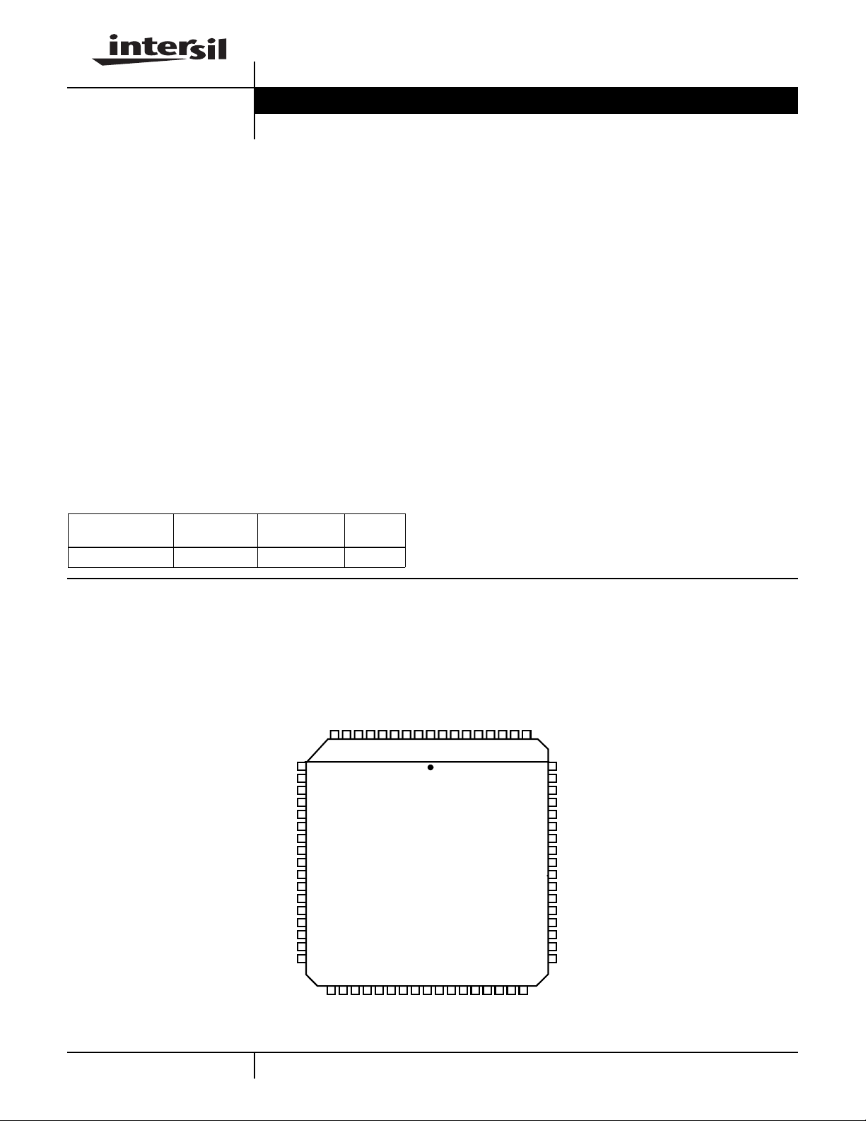
Pinout
VUP1
SG_1
VLOW1
V
GNDA1
GNDD1
CC1
XTEN1+
XTEN1CTC1-10K
CTC1-27K
LASERON1B
OC1
TECFB1
TECREF1
TECGDR1
TRES1
HIP9022 (PLCC)
TOP VIEW
ESD LASER GND
ESD LASER GND
ESD SHUNT DRAIN-1
ESD SHUNT DRAIN-1
ESD SHUNT DRAIN-1
ESD LASER PS-1
ESD LASER PS-1
VDDNC
10
11
12
13
EE
14
15
16
17
18
19
20
21
22
23
24
25
26
27 28 29 30 31 32 33
NC
OT1
INVERT
RESETB
DIAGINB
NULLB
ESD SHUNT DRAIN-2
123456789
68 67 66 65 64 63 62 61
34
IN
A3
CC
NC
V
V
SB_H
ESD SHUNT DRAIN-2
ESD SHUNT DRAIN-2
ESD LASER PS-2
ESD LASER PS-2
RLY_IN
RLY_OUT
V9P
434241403938373635
A0
A1
A2
DIAG
NC
TECREFR
60
59
58
57
56
55
54
53
52
51
50
49
48
47
46
45
44
VUP2
SG_2
VLOW2
GNDA2
GNDD2
CC2
XTEN2+
XTEN2CTC2-10K
CTC2-27K
LASERON2B
OC2
TECFB2
TECREF2
TECGDR2
TRES2
OT2
4-1
CAUTION: These devices are sensitive to electrostatic discharge; follow proper IC Handling Procedures.
http://www.intersil.com or 407-727-9207
| Copyright © Intersil Corporation 1999
Page 2

X
HIP9022
+12V
1µF
NC
VUP1
SG_1
VLOW1
-5V
1µF
V
EE
GNDA1
GNDD1
CC1
XTEN1+
XTEN1-
CTC2-10K
CTC1-27K
LASER_ON1B
OC1
TECFB1
TECREF1
TECGDR1
TRES1
OT1
NC
INVERT
ESD
LASERPS-1
7
8
V
V
DD
DD
9
10
11
12
13
14
15
16
17
18
19
20
21
PU
22
23
24
25
26
27
28
29 30 31 32 33
RESETB
DIAGINB
SHUNT
DRAIN-1
56
9V REG.
V/I REF.
LASER DRIVER-1
PUPU PUPDPD
NULLB
ESD
4
V9P
SB_H
3
LD1
34
NC
ESD
LASER
GNDGND
12
SAMPLE/HOLD
SYSTEM
35 37 38 39 40
V
IN
ESD
SHUNT
DRAIN-2
68
LD2
36
V
A3 A2 A1 A0
CC
+5V
LASERPS-2
6667
ESDD2ESDD1
LASER
GATE
DRIVE
A5
12kΩ
30kΩ
PU PU PU PU
ESD
65
64
A4
+
-
OTA GATE
DRIVE AMP.
+
-
A2
CURRENT
MONITOR
1kΩ
AMP.
A1
ON/OFF
O. C.
COMP.
TEC DRIVER
(THERMO
ELECTRIC
COOLER
CIRCUIT)
AND
OVER/UNDER
TEMPERATURE
COMPARATOR
LASER DRIVER-2
V
TEST
OUT
DIAG
A3
+
-
11kΩ
11kΩ
V
CC
+
-
X10
THERM.
COMP
+
-
+
-
41 42
A6
PU
1.9V
NC
63
RLY_IN
PD
62
RLY_OUT
V9P
61
60
VUP2
59
SG_2
58
VLOW2
57
GNDA2
56
GNDD2
55
CC2
54
XTEN2+
53
XTEN2-
52
CTC2-10K
51
CTC2-27K
50
LASER_ON2B
49
OC2
48
TECFB2
47
TECREF2
46
TECGDR2
45
TRES2
44
OT2
NOTE:
PU = 60kΩ PULLUP RESISTOR
PD = 60kΩ PULLDOWN RESISTOR
= SCHMITT TRIGGER HYSTERESIS
43
TECREFR
(TEMP. REF.
RESISTOR)
5 - 10kΩ
V
CC
+9V
1µF
1µF
1µF
0.1µF
0.1µF
(THERMO-RESISTOR
SENSES LASER TEMP.,
NEG. TEMP. COEF.,
TEC COOLS LASER.)
TO V
CC
TO GND
LASER P.S.
3 TO 5V
Q3
RF3V49092
Q2
0.02µF
RFD3055
OR
EQUIV.
RELAY1
LASER
I
DL
R
S
0.25Ω
TEC P.S.
3V
Q1
TEC
X
THERMAL RELATED COMPONENTS
FIGURE 1. HIGH SPEED LASER DRIVER FUNCTIONAL BLOCK DIAGRAM SHOWN IN QUIESCENT P.S. CURRENT TEST MODE
4-2
Page 3

HIP9022
Pin Descriptions
PIN
NUMBER SYMBOL DESCRIPTION
1, 2 ESD LASER GND Laser supply and system ground.
3, 4, 5 ESD SHUNT DRAIN-1 Laser diode ESD protection.
6, 7 SD LASER PS-1 Laser power supply ESD protection.
8VDDInput for 12V power supply.
9 NC No connection.
10 VUP1 Filter capacitor for internally generated shunt gate upper voltage level (1µF).
11 SG_1 Drive output to shunt Power FET gate.
12 VLOW1 Filter capacitor for internally generated shunt Power FET gate lower drive voltage level (1µF).
13 V
14 GNDA1 Analog Ground.
15 GNDD1 Digital Ground.
16 CC1 Gate drive to the current source Power FET.
17 XTEN1+ Times 10 constant current monitor amplifier input from the high side of the sense resistor.
18 XTEN1- Times 10 constant current monitor amplifier input from the low side of the sense resistor.
19 CTC1-10K Thermal compensation short time constant where TTC= External C x 10kΩ. (External C typically equal
20 CTC1-27K Thermal compensation long time constant where TTC= External C x 27kΩ. (External C typically equal
21 LASERON1B Input control turns shunt Power FET gate drive ON/OFF with 5V CMOS logic. Low turns the shunt Power
22 OC1 Laser over-current indicator flag.
23 TECFB1 Feedback to stabilize the TEC loop.
24 TECREF1 Feedback to stabilize the TEC loop.
25 TECGDR1 Thermo-Electric Cooler Power FET gate drive.
26 TRES1 Thermo-Resistor output to ground connection for TEC control.
27 OT1 Laser out of temperature range indication.
28 NC No connection.
29 INVERT High input converts to operation with Pmos Current source and NDmos shunt Power FET external
30 RESETB WhenRESETB is held low,three reset actions occur. The LASERONB input is defeated to a Laser Off con-
31 DIAGINB Low level activates the diagnostic mode. This pin has an internal pull-up.
32 NULLB Auto-zeros the S/H amplifier selected by address when held low. This pin has an internal pull-up.
33 SB_H Samplesthe selected address when held low.The setup time for address is <25ns. This pin has an internal
34 NC No connection.
35 V
36 V
37 A3 Refer to the Table 1 Address Map. The A3 - A0 pins have an internal pull-up.
EE
IN
CC
Input for -5V power supply.
0.02µF).
0.1µF).
FET OFF and the Laser ON. These pins have an internal pull-up.
transistors. Low input converts to operation with NDmos Current source and Pmos high side shunt Power
FET external transistors. This pin has an internal pull-down.
dition. The SG_1, 2 outputs are switched to VLOW when in the INVERT low mode and to VUP when in the
INVERT high mode. The TEC amplifier is turned off to switch the TECGDR1, 2 outputs to Ground. This pin
has an internal pull-down.
pull-up.
Analog voltage sampled by selected S/H. The input voltage range is 0 to 5V. There is an internal voltage
clamp for voltage outside of this range. There is an internal 2 - 3µs filter for noise rejection.
Input for 5V power supply.
4-3
Page 4

HIP9022
Pin Descriptions
PIN
NUMBER SYMBOL DESCRIPTION
38 A2 Refer to the Table 1 Address Map. The A3 - A0 pins have an internal pull-up.
39 A1 Refer to the Table 1 Address Map. The A3 - A0 pins have an internal pull-up.
40 A0 Refer to the Table 1 Address Map. The A3 - A0 pins have an internal pull-up.
41 DIAG Diagnostic output, A 0V - 5V analog signal output limits internally to a range of -0.3V to 5.3V. The output is
42 NC No connection.
43 TECREFER External resistor to ground with a resistor value equal to the valueof the thermo-resistor at the desired laser
44 OT2 Laser out of temperature range indication.
45 TRES2 Thermo-Resistor output to ground connection for TEC control.
46 TECGDR2 Thermo-Electric Cooler Power FET gate drive.
47 TECREF2 Feedback to stabilize the TEC loop.
48 TECFB2 Feedback to stabilize the TEC loop.
49 OC2 Laser over-current indicator flag.
50 LASERON2B Input control turns shunt Power FET gate drive ON/OFF with 5V CMOS logic. Low turns the shunt Power
51 CTC2-27K Thermal compensation long time constant where TTC= External C x 27kΩ. (External C typically equal
52 CTC2-10K Thermal compensation short time constant where TTC= External C x 10kΩ. (External C typically equal
53 XTEN2- Times 10 constant current monitor amplifier input from the low side of the sense resistor.
54 XTEN2+ Times 10 constant current monitor amplifier input from the high side of the sense resistor.
55 CC2 Gate drive to the current source Power FET.
56 GNDD2 Digital Ground.
57 GNDA2 Analog Ground.
58 VLOW2 Filter capacitor for internally generated shunt Power FET gate lower drive voltage level (1µF).
59 SG_2 Drive output to shunt Power FET gate.
60 VUP2 Filter capacitor for internally generated shunt gate upper voltage level (1µF).
61 V9P Filter capacitor bypass for internally generated 9V power source (1µF).
62 RLY_OUT Relay output drive from an N-channel FET controls an external relay to switch the Laser power supply or
63 RLY_IN Relay input control with 5V CMOS logic. A high switches on the relay. This pin has an internal pulldown.
64, 65 ESD LASER PS-2 Laser power supply ESD protection.
66, 67, 68 ESD SHUNT DRAIN-2 Laser diode ESD protection.
(Continued)
the channel addressed by A0 - A3.
temperature. (Typically in the 5kΩ to 10kΩ range)
FET OFF and the Laser ON. These pins have an internal pull-up.
0.1µF).
0.02µF).
power supply interlock ON/OFF for both Laser Drivers.
4-4
Page 5

HIP9022
Absolute Maximum Ratings Thermal Information
Maximum Analog Supply Voltage, VDD . . . . . . . . . . . -0.3V to 14V
Logic Supply Voltage, VCC. . . . . . . . . . . . . . . . . . . . . . -0.3V to 6V
Analog Negative Supply Voltage, VEE . . . . . . . . . . . . . 0.3V to -5.5
Maximum Laser Protection Diode Current . . . . . . . . . . 10A, 200ns
Operating Conditions
VDD Supply Voltage Range, VDD . . . . . . . . . . . . . . 11.4V to 12.6V
VCC Supply Voltage Range, VCC . . . . . . . . . . . . . . . . 4.5V to 5.5V
VEE Supply Voltage Range, VEE. . . . . . . . . . . . . . . . -4.5V to -5.5V
Laser Power Supply Range, V
TEC Power Supply Range, V
Laser Operating Current Range, IDL. . . . . . . . . . . . . . . . . 0A to 2A
TEC Operating Current Range, I
CAUTION: Stresses above those listed in “Absolute Maximum Ratings” may cause permanent damage to the device. This is a stress only rating and operationofthe
device at these or any other conditions above those indicated in the operational sections of this specification is not implied.
NOTE:
1. θJA is measured with the component mounted on an evaluation PC board in free air.
. . . . . . . . . . . . . . . . . . 3V to 5V
LAS
. . . . . . . . . . . . . . . . . . . 3V to 5V
TEC
. . . . . . . . . . . . . . . . . 0A to 2A
TEC
Thermal Resistance (Typical, Note 1) θJC(oC/W)
PLCC Package. . . . . . . . . . . . . . . . . . . . . . . . . . . . . 40
Maximum Operating Junction Temperature, TJ. . . . . . . . . . . 100oC
Maximum Storage Temperature Range, T
. . . . -55oC to 150oC
STG
Maximum Lead Temperature (Soldering 10s) . . . . . . . . . . . . 300oC
Die Characteristics
Back Side Potential . . . . . . . . . . . . . . . . . . . . . . . . . -VEE, Substrate
Electrical Specifications T
= 100οC, VDD = 12V, VCC = 5V, VEE = -5V, INVERT Low (Figure 1 Configuration)
J
Unless Otherwise Specified
PARAMETER SYMBOL TEST CONDITIONS MIN TYP MAX UNITS
POWER SUPPLIES
V9P Voltage, No External Load V9P 1µF Tantalum
-9-V
Capacitor to V9P
V9P Thermal Shutdown 150 - V9P Thermal Shutdown Recovery - - 125
o
o
V9P Current Limiting 65 - - mA
Power Supply Current I
V
DD
V
Power Supply Current I
CC
Power Supply Current I
V
EE
DD
CC
EE
-2575mA
- 1.5 25 mA
-75 -23 - mA
LOGIC/DIGITAL INPUTS (A0-A3,NULLB and SB_H, LASERON1B, LASERON2B with 60kΩ Pullup Resistors; INVERT,RESETB,RLY_IN 60kΩ
with Pulldown Resistors)
Low Level Input Voltage V
High Level Input Voltage V
Minimum Hysteresis V
Low Level Input Current (Inputs with Pullups) I
High Level Input Current (Inputs with Pulldowns) I
IL
IH
HYS
IL
IH
0 - 1.5 V
3.5 - VCC+ 0.3 V
0.3 - - V
-140 - - µA
- - 140 µA
CONSTANT CURRENT CONTROLLER
OTA Gate Drive Amp. (A2) Voltage Output Range V
Current Monitor Amp. (A1) Gain A
Current Monitor Amp. Differential Sense Input Range V
Current Monitor Amp. Input Offset V
Current Monitor Amp. Common Mode Input Range V
SHUNT CURRENT SWITCH CONTROLLER (Note 2) V
UPPER
G
VS
IN
IO
IC
= 2V, V
= -1V, Gate Load = 5000pF, VUP1, 2; 1µF Filter Capacitor to
LOWER
-4 - V
CC
9.8 10 10.2 0 - 500 mV
-5 - 5 mV
0-5V
GND, VLOW1, 2; 1µF Filter Capacitor to GND, Unless Otherwise Specified
Shunt Gate Output Rise/Fall time t
R/tF
10% -90% Rise,
- - 20 ns
90% -10% Fall
Propagation Delay, LASERONB1, 2 to SG_1, 2 t
Drive Output Voltage V
UPPER
V
LOWER
TJ = 100oC - 80 110 ns
D
= -25oC - 60 95 ns
T
J
0-VCCV
-4 - V
CC
C
C
V
V
4-5
Page 6

HIP9022
Electrical Specifications T
= 100οC, VDD = 12V, VCC = 5V, VEE = -5V, INVERT Low (Figure 1 Configuration)
J
Unless Otherwise Specified (Continued)
PARAMETER SYMBOL TEST CONDITIONS MIN TYP MAX UNITS
Driver Maximum Output Current I
Shunt Controller Switching Frequency f
DRSW
SC
-1 - 1 A
0 - 2.5 MHz
ANALOG SAMPLE/HOLD AMPLIFIERS
Low Level Input Voltage V
Low Level Input Current I
High Level Input Voltage V
Minimum Hysteresis V
Analog Input Voltage Range V
IL
IL
IH
HYS
IN
0 - 1.5 V
-140 - - µA
3.5 - VCC+ 0.3 V
0.3 - - V
0-V
- 0.2 V
CC
Minimum Sample/Hold Pulse Width - 10 - µs
Droop Rate, Constant Current Addresses #’s 1, 2 - - 0.006 V/s
Droop Rate, Other Addresses #’s 3 - 8 - - 0.06 V/s
Maximum Analog Multiplexing Frequency - - 30 kHz
DIAGNOSTIC OUTPUT (DIAG Output)
Voltage Follower Voltage Range V
Voltage Follower Maximum Clamp Voltage V
CL
O
0-V
--V
- 0.2 V
CC
+ 0.3 V
CC
O. C. (OVER CURRENT) COMPARATOR (OC1, 2 Outputs)
Threshold (%) O.C. Detection Programmed Current
- 140 - %
as Ref.
Output Voltage, Low Level V
Output Current, Low Level I
Output Voltage, High Level V
Output Current, High Level I
OL
OL
OH
OH
0 - 1.5 V
-12-mA
3.5 - VCC- 0.5 V
-4-mA
TEC REF. RESISTOR AND DRIVE OUTPUT
TECREFR Output Voltage to Reference Resistor V
TECGDR1, 2 Drive Output Voltage V
REFR
TECG
1.71 1.9 2.09 V
0-9V
OVER/UNDER TEMPERATURE COMPARATOR (To OT Output)
Under Temp. Limit T
Over Temp. Limit T
Output Voltage, Low Level V
Output Current, Low Level I
Output Voltage, High Level V
Output Current, High Level I
LOW
HIGH
OL
OL
OH
OH
2.07 2.1 2.13 V
1.67 1.7 1.73 V
0 - 1.5 V
-12-mA
3.5 - VCC- 0.5 V
-4-mA
RELAY DRIVER
Driver Output Current I
Drain to Source Resistance r
RLY
DS(ON)
- - 30 mA
-20-Ω
LASER PROTECTION DIODES See Figure 1
Maximum Diode Forward Voltage Drop V
Maximum Reverse Diode Current I
V
ESDX
LDX
10A Peak Current - - 2 V
LDX,
--1µA
NOTE:
2. The drive control sets the high and low voltages to the gate of the Power FET driver (shunt switch). Both the upper and lower levels are set by
values held in two of the sample/hold amplifiers. External capacitors at VUP1, 2 and VLOW1, 2 are required for stabilization.
4-6
Page 7

Address, Timing and Waveforms
DIGITAL
CONTROL
HIP9022
S/H
INT. TEST
TEST NULL OR S/H
ADDRESS NUMBERS
SAMPLE
(SH_B INPUT)
NULLB
INPUT
V
INPUT
DIAGNOSTIC
(DIAGINB INPUT)
IN
#11 to 14 #15#1 to 8 #1 to 8#1 to 8 #1 to 8
#9 or 10
(NULL OR S/H) (RESET)
FIGURE 2. ADDRESS WITH SAMPLE, NULL, VIN AND DIAGONAL WAVEFORMS
TABLE 1. HIP9022 ADDRESS MAP
ADDRESS
A3 A2 A1 A0
NO.
0000 1 ANALOG V
0001 2 ANALOG V
0010 3 ANALOG V
0011 4 ANALOG V
0100 5 ANALOG V
0101 6 ANALOG V
0110 7 ANALOG V
0111 8 ANALOG V
FUNCTION
TYPE FUNCTION NAME
Voltage for Constant Current Level, Laser Driver #1
IN(DL)
Voltage for Constant Current Level, Laser Driver #2
IN(DL)
Level, Laser Driver #1
LOWER
Level, Laser Driver #2
LOWER
Level, Laser Driver #1
UPPER
Level, Laser Driver #2
UPPER
Thermal Compensation Level, Laser Driver #1
IN(DL)
Thermal Compensation Level, Laser Driver #2
IN(DL)
1000 9 DIGITAL Test Mode: S/H Amp, Auto Zero Null Voltage (Note 4)
1001 10 DIGITAL Test Mode: S/H Amp Output Voltage (Note 4)
1010 11 DIGITAL Test Mode: Set VUP and V
Amps to Three-State (Note 4)
LOW
1011 12 DIGITAL VLOW#1 Set to Positive Output (Default is Negative)
1100 13 DIGITAL VLOW#2 Set to Positive Output (Default is Negative)
1101 14 DIGITAL Thermal Compensation Activated (Default is Deactivated)
1110 15 DIGITAL Reset Digital Address (9-14) to Default State
1111 16 DIGITAL Idle Condition (S/H Pin Defeated) (Note 3)
NOTES:
3. The Idle address is protective in that SB_H input noise cannot disturb the chip if the Idle address is selected; also, the Address inputs are High
(selecting Idle state) if the pins are open.
4. Address Numbers 9 - 11 are shaded to indicate test mode conditions and are shown for information only. These addresses are used in original
production testing and not required for user applications. However, note that Address No. 15 will force a reset for Address Numbers 9 - 14.
5. DigitalProgramming: To set the digital addresses, only the proper digital address and a negative pulse >100ns on SB_H is needed. To reset the
digital addresses to the default states, Address 15 and a SB_H pulse >100ns is needed. Normally the digital addresses will be set first, and the
analog addresses programmed next. The test modes, Address Numbers 9 - 11, will normally only be used during factory testing. An address
15 Reset should normally precede most programming in order to assure that the digital address states begin in their default state. Otherwise,
the digital address states will be undefined because there is no power-up-reset.
6. Analog Programming: To program the eight S/H circuits, addresses of 0-5V analog signal on VINand negative pulses on NullB (10µs) and SB_H
(20µs) pins are needed. The NullB pulse is valid only during the SB_H pulse and should occur during the first half of the SB_H pulse. The S/H
amplifier is auto-zeroed for zero offset when both NullB and SB_H are low.The input VINis captured on the S/H storage capacitor during SB_Hlow.
7. The Diagnostic mode reads map addresses 1 - 8 via the DIAG output when DIAGINB is low.
4-7
Page 8

HIP9022
Circuit Block Descriptions
Laser Drive Circuitry
In Figure 3, the gate of the external current source Power
FET, Q2 is driven via the Operational Transconductance
Amplifier (OTA), A2 on the IC. The voltage on the current
sense resistor, RS in the source of the Power FET is
monitored by a X10 gain of the feedback amplifier, A1. The
stability of the current loop is established with an external
0.1µF capacitor to ground at the gate of the PowerFET. The
sampled voltage range is 0 to 0.5V when the proper value of
sense resistor, RS is chosen (typically 0.25Ω for 2A). The
OTA, A2 compares the X10 gain signal toa0to5Vreference
signal from an on-chip Sample and Hold (First S/H) circuit.
The Q2 drain current (Laser Drive current), IDL is:
V
I
DL
where V
voltage reference signal.
The S/H reference for the Laser Drive Current current is
updated with other multiplexed S/H circuits from a serial bus
and an off-chip D/A converter. Laser constant current is fully
controllable by the multiple x analog S/H b us, allo wing accur ate
calibration of the laser output and corrections as the laser ages.
In Figure 1, the laser drive current from Q2 is digitally switched
to either flow through or is shunted around the laser diode by
switchingthe external Shunt Pow erFET, Q3 on or off. The gate
of the Shunt FET is switched between two voltages (Upper and
Lower) which are provide by 2nd and 3rd S/H circuits. These
Shunt FET gate drive levels are fully progr ammab le via the
multiplexed analog S/H b us . By adjusting these le vels to
account for the laser power supply, the Shunt FET threshold
and channel resistance; minimum Shunt FET gate drive power
levels can be established. The Upper and Lo w er gate v oltage
driver circuits are two high current OTA amplifiers with two filter
capacitors. The upper voltage is programmab le in the 0V to
V
programmablein the range of -4V to VCC. The -4V extension is
accomplished by an optional on-chip voltage inv erter circuit.
The input to amplifier A3 is either direct from the S/H input or
inverted by amplifier A5.
The maximum laser on-off switching speeds are dependent
on the selection of Shunt FETs. A Harris dual
complementary MOSFET, RF3V49092 or RF3S49092 has
been designed specifically for this application. With the
constant current set at 0.8A, a typical laser switching speed
of 20ns has been measured.
Thermal Compensation
A 4th S/H circuit is used to set the amplitude of an optional
thermal compensation signal which can be used to
modulate the constant laser current source as a two pole
filtered effect of the laser on-off data. This feature may be
disabled when it is not required. This circuit is designed to
compensate for the temperature variations in the laser as
the laser is tur ned on and off. The bypass capacitors at the
Thermal Comparator(CTCx-10K, CTCx-27K) represent the
respective poles for the filter.
IN DL()
-------------------------=
RS10×()
is the programmed VIN for the First S/H
IN(DL)
range at the input of amplifier A4. The lower voltage is
CC
(EQ. 1)
A laser cools after it has been off for a period of time and is
more efficient when it is turned-on. Compensation for the
increased efficiency is made by slightly reducing the
current level of the constant current source FET. The level
will be reduced by a programmable amount of 0 to 5% of
full scale. The programmable amount is fixed by the level of
compensation to S/H addresses 7 and 8 (see Table 1). The
percent of modulation (change) in drive current is
calculated as follows:
Modulation °°⁄
IN TC()
---------------------
V
IN DL()
5°°⁄×=
(EQ. 2)
V
For example, if we control the Laser Drive current with 2V
programmed with address 1 and 2 for the First S/H’s, given
that V
= V
I
DL
= 2V and RS = 0.25Ω. Then, from EQ. 1,
IN(DL)
/(RS x 10) = 2/(0.25 x 10) = 0.8A.
IN(DL)
If 2V is programmed to addresses 7 and 8 as Thermal
Compensation, V
for the 4th S/H’s, then,
IN(TC)
Mod.% = (2/2) x 5% = 5%.
In Figure 3, the correction is applied from the output of the
Thermal Compensation circuit (where the current is
2V/20kΩ = 0.1mA) to the input of amplifier A2. The 0.1mA is
forced into the 1kΩ resistor (and the low Z output of A1) to
increase the voltage at the inverting input of A2 by 0.1V or 5%
of the +V
by the 0 to V
input (2V) to A2. The modulation input is limited
IN(DL)
input range of S/H maximum VIN.
CC
Input Data
Q2
A2
+
-
A1
1kΩ
12kΩ
30kΩ
X10
+
-
VOLT. TO
CURRENT
27kΩ
+
-
O. C.
COMP.
-
THERMAL
COMP.
VOLT. TO
CURRENT
20kΩ
S/H SYS
FIGURE 3. LASER CONSTANT CURRENT SOURCE DRIVER
WITH OVER CURRENT DETECTION AND
THERMAL COMPENSATION
+
10kΩ
55
CC2
54
XTEN2+
53
XTEN2OC2
49
CTC2-27K
51
CTC2-10K
52
0.1µF
0.02µF
0.1µF
0.25Ω
R
S
4-8
Page 9

HIP9022
Both analog and digital data is input to control the action of
the dual laser driver. Address codes and input data are
described in the Table 1 Address Map. Digital data is
normally entered first, followed by the analog data via the
multiplexed analog bus which updates the S/H stored
voltage levels. Four bit digital addresses to pins A3, A2, A1
and A0 are decoded to define the programming functions
for data input. It is important to note that Address 15 is a
reset for Addresses 9 - 14 and should be performed as the
first step in programming because there is no power-onreset on-chip.
Diagnostic Output Data
For the purpose of monitoring on-chip signals, the
multiplexed bus can be used to output signals (at the DIAG
pin) via an analog diagnostic amplifier. This mode has the
capability to monitor the multiplexed output of four (0-5V)
analog signals for each laser channel. Note that the
diagnostic information at the VLOW (Amplifier A3) output is
2:1 resistor divided to +5V (V
) to return this signal to a 0
CC
to 5V range. To minimize noise problems the monitoring
function is normally performed during the laser scan for only
one signal per scan. In addition, there are 3 test modes
which allows the bus to present analog signals for testing the
performance of the eight S/H circuits.
Thermo-Electric-Cooler (TEC) Circuitry
Figure 4 shows the Thermal Electric Cooler (TEC) drive
circuit with an external reference resistance, a thermoresistor to sense temperature plus feedback components for
stable drive. There is a thermo-resistor reference input on
the chip for monitoring the laser's temperature via a 5-10kΩ
thermo-resistor which must be mounted near the laser. A
reference voltage on the external reference resistor is
established by a current from a stable bias source. This
current is mirrored to the thermo-resistor (one for each laser
driver system). A comparator senses the voltage across the
reference resistor versus the voltage across the thermo-
resistor and drives the gate of the TEC FET driver. As such,
the TEC circuit senses the thermo-resistor input as a
measure of the laser temperature and the TEC drive is
adjusted to maintain a stable Laser temperature slightly
below the ambient temperature. An external Power FET is
needed to provide the high TEC driver currents. An out of
range temperature output for each laser is also provided.
Laser Protection Diodes
Another feature included on the chip is two high current ESD
diodes which, in the printer system, are used to protect the
Laser Diodes from ESD damage. Another component of Laser
protection in printer systems are relays to disconnect the
Lasers when in a non-operating mode. For this purpose, a
single relay driver is included.
Over Current Flag Output (OC1, OC2)
Over-current detection is also included on-chip. The circuit of
Figure 3 shows the over current detection circuit. F or each
laser source current driver,the overcurrent monitor compares
the S/H input of amplifier A2 to the output of amplifier A1. If
the output voltage of A1 exceeds the input of A2 by 40%, then
an over current state exists and the OC output will go high.
Invert Option
An INVERT input reconfigures the device such that the
constant current source can be high side instead of the
normal low side. This provides functionality for driving laser
diodes in a common cathode configuration as opposed to
the normal common anode configuration. The INVERT must
be low (or open with the internal pull down) for the Figure 1
circuit.
Reset Action
The RESETB (active low) controls three things:
(1) The TEC driver is turned off.
(2) The Shunt driver is turned on to turn off the laser.
(3) The Constant current driver is turned off.
+
CURRENT
MIRROR
12
1.9V
+
-
O.T.
U.T.
FIGURE 4. TEC (THERMAL ELECTRIC COOLER) CIRCUIT WITH REFERENCE RESISTOR AND THERMAL RESISTOR SENSOR OF
LASER TEMPERATURE
+
-
TEMP.
COMP.
-
+
48
47
46
45
44
43
TECFB2
TECREF2
TECGDR2
TRES2
OT2
TECREFR
Q2
TEC
REFERENCE
RESISTOR
+
LASER2
THERMORESISTOR
(TEMPERATURE SENSOR)
THERMALLY
COUPLED
COMPONENTS
4-9
Page 10

HIP9022
Plastic Leaded Chip Carrier Packages (PLCC)
0.042 (1.07)
0.048 (1.22)
PIN (1) IDENTIFIER
0.020 (0.51) MAX
3 PLCS
C
L
D1
D
0.026 (0.66)
0.032 (0.81)
0.045 (1.14)
MIN
0.042 (1.07)
0.056 (1.42)
0.050 (1.27) TP
VIEW “A” TYP.
C
L
EE1
0.013 (0.33)
0.021 (0.53)
0.025 (0.64)
MIN
0.004 (0.10) C
0.025 (0.64)
0.045 (1.14)
D2/E2
D2/E2
A1
A
-C-
VIEW “A”
0.020 (0.51)
MIN
SEATING
PLANE
N68.95 (JEDEC MS-018AE ISSUE A)
68 LEAD PLASTIC LEADED CHIP CARRIER PACKAGE
R
SYMBOL
A 0.165 0.180 4.20 4.57 -
A1 0.090 0.120 2.29 3.04 -
D 0.985 0.995 25.02 25.27 D1 0.950 0.958 24.13 24.33 3
D2 0.441 0.469 11.21 11.91 4, 5
E 0.985 0.995 25.02 25.27 E1 0.950 0.958 24.13 24.33 3
E2 0.441 0.469 11.21 11.91 4, 5
N68 686
INCHES MILLIMETERS
NOTESMIN MAX MIN MAX
Rev. 2 11/97
NOTES:
1. Controllingdimension: INCH. Converted millimeterdimensionsare
not necessarily exact.
2. Dimensions and tolerancing per ANSI Y14.5M-1982.
3. DimensionsD1 and E1 do not include mold protrusions. Allowable
mold protrusion is 0.010 inch (0.25mm) per side. Dimensions D1
and E1 include mold mismatch and are measured at the extreme
material condition at the body parting line.
4. To be measured at seating plane contact point.
-C-
5. Centerline to be determined where center leads exit plastic body.
6. “N” is the number of terminal positions.
All Intersil semiconductor products are manufactured, assembled and tested under ISO9000 quality systems certification.
Intersil semiconductor products are sold by description only. Intersil Corporation reserves the right to make changes in circuit design and/or specifications at any time without notice. Accordingly, the reader is cautioned to verify that data sheets are current before placing orders. Information furnished by Intersil is believed to be accurate and
reliable. However,no responsibility is assumed by Intersil or its subsidiaries for its use; nor for any infringements of patents or other rights of third parties which may result
from its use. No license is granted by implication or otherwise under any patent or patent rights of Intersil or its subsidiaries.
For information regarding Intersil Corporation and its products, see web site http://www.intersil.com
Sales Office Headquarters
NORTH AMERICA
Intersil Corporation
P. O. Box 883, Mail Stop 53-204
Melbourne, FL 32902
TEL: (407) 724-7000
FAX: (407) 724-7240
EUROPE
Intersil SA
Mercure Center
100, Rue de la Fusee
1130 Brussels, Belgium
TEL: (32) 2.724.2111
FAX: (32) 2.724.22.05
ASIA
Intersil (Taiwan) Ltd.
7F-6, No. 101 Fu Hsing North Road
Taipei, Taiwan
Republic of China
TEL: (886) 2 2716 9310
FAX: (886) 2 2715 3029
4-10
 Loading...