

Page 1
HIP7038A8
PRELIMINARY
April 1994
Features
• Direct Replacement for HIP7030A2/A8 Microcontrollers
- All Hardware and Software Features
- Equivalent Timing and Performance
• Memory
- 176 Bytes of RAM
- 7744 Bytes of Programmable EEPROM
- 242 Bytes of Bootstrap Program
• Single 5V Supply
• 10MHz Operating Frequency (5.0MHz Internal Bus
Frequency) at 5V.
• 28 Lead Small Outline Ceramic Package
- Same Terminal Assignment as HIP7030A2
and HIP7030A8
J1850 8-Bit 68HC05 Microcontroller
8K EEPROM Version
Description
The HIP7038A8 HCMOS Microcomputer is an EEPROM
version of the HIP7030A family of low-cost single-chip J1850
microcontrollers. These microcontrollers provide the system
designer with a complete set of building blocks for implementing a “Class B” VPW multiplexed communications
network interface, which fully complies with SAE Recommended Practice J1850. The HIP7038A8 contains all hardware and software features of the HIP7030A2/A8
microcontrollers with equivalent timing, performance characteristics, and an identical footprint.
The device can be programmed using the HIP7038A8
EEPROM Programmer available from Intersil. In-circuit
Emulation Tools are also provided for system development.
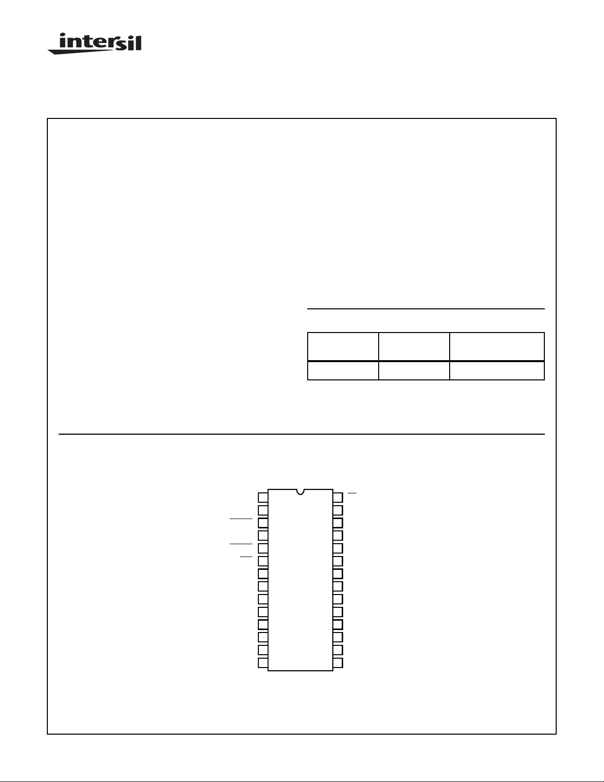
Ordering Information
TEMPERATURE
PART NUMBER
HIP7038A8F -40oC to +85oC 28 Lead Ceramic SOIC
RANGE PACKAGE
Pinout
HIP7038A8 (SOIC FLATPACK)
TOP VIEW
1
TCAP
2
TCMP
IRQ
V
PA7
PA6
PA5
PA4
PA3
PA2
PA1
DD
3
4
5
6
7
8
9
10
11
12
13
14
VPWIN
VPWOUT
RESET
28
SS
MISO
27
MOSI
26
25
SCK
24
OSCIN
23
OSCOUT
V
22
21
PD0
20
PD1
19
PD2, V2
18
PD3, V3
17
PD4, VREF
16
OSCB
15
PA0
SS
CAUTION: These devices are sensitive to electrostatic discharge; follow proper IC Handling Procedures.
407-727-9207
| Copyright © Intersil Corporation 1999
9-99
File Number
3647.1
Page 2
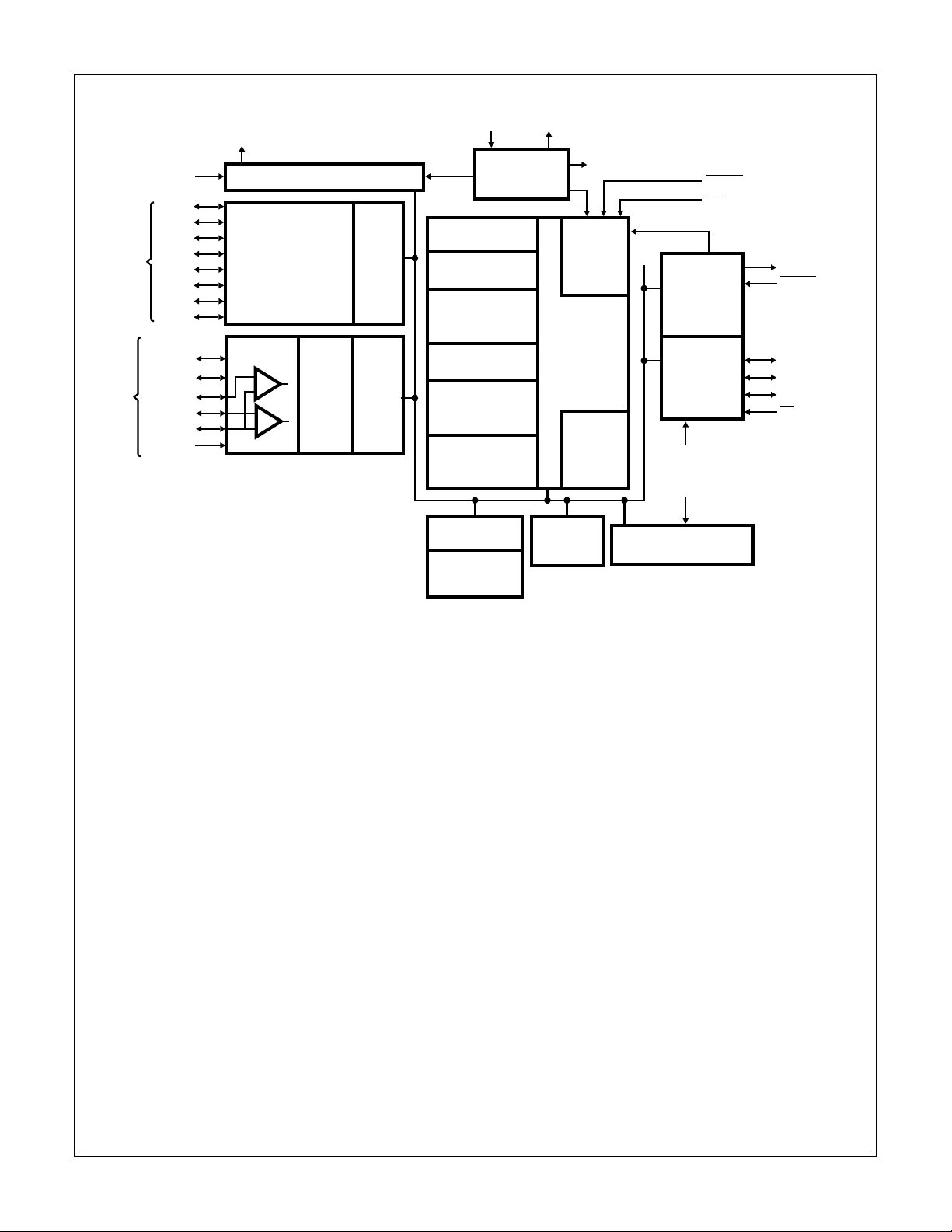
Block Diagram
1
TCAP
15
PA0
14
PA1
13
PA2
12
PA3
11
PA4
10
PA5
9
PA6
PORT A I/O LINES
PD2, V2
PD3, V3
PD4, VR
PORT D I/O LINES
PA7
PD0
PD1
TCAP
8
21
20
19
18
17
TCMP
PORT D
VSS22
VDD7
2
TIMER SYSTEM
PORT
A
REG
REG
+
-
+
-
PORT D
SFR
REG
DATA
DIR
REG
PORT D
DIR
REG
HIP7038A8
INTERNAL
PROCESSOR
CLOCK
ACCUMULATOR
8
REGISTER
8
CONDITION
REGISTER
5
POINTER
6
PROGRAM
COUNTER
5
PROGRAM
COUNTER
8
7744 x 8
EEPROM
242 x 8
BUILT-IN-TEST
EEPROM
OSCIN OSCOUT
OSCILLATOR
AND
÷ 2
A
INDEX
X
CODE
CC
STACK
S
HIGH
PCH
LOW
PCL
STATIC RAM
2324
CONTROL
176 x 8
16
OSCB
SYMBOL INT
CPU
CPU
ALU
WATCHDOG AND
SLOW CLOCK DETECT
5
RESET
6
IRQ
VPW SYMBOL
ENCODER /
DECODER
AND
ARBITRATION
SPI
SYSTEM
INTERNAL
PROCESSOR
CLOCK
4
3
25
26
27
28
VPWOUT
VPWIN
SCK
MOSI
MISO
SS
9-100
Page 3

Specifications HIP7038A8
Absolute Maximum Ratings Thermal Information
Supply Voltage (VDD) . . . . . . . . . . . . . . . . . . . . . . . . . -0.3V to +6.0V
Input or Output Voltage
Pins with VDD Diode . . . . . . . . . . . . . . . . . . . . -0.3V to VDD +0.3V
Pins without VDD Diode. . . . . . . . . . . . . . . . . . . . . -0.3V to +10.0V
Current Drain Per Pin, I (Excluding VDD and VSS) . . . . . . . . 25mA
ESD Classification . . . . . . . . . . . . . . . . . . . . . . . . . . . . . . . . Class 2
Gate Count. . . . . . . . . . . . . . . . . . . . . . . . . . . . . . . . . . 21000 Gates
CAUTION: Stresses above those listed in “Absolute Maximum Ratings” may cause permanent damage to the device. This is a stress only rating and operation
of the device at these or any other conditions above those indicated in the operational sections of this specification is not implied.
Operating Conditions
Operating Voltage Range. . . . . . . . . . . . . . . . . . . . . +4.5V to +5.5V
Operating Temperature Range. . . . . . . . . . . . . . . . . -40oC to +85oC
Input Low Voltage. . . . . . . . . . . . . . . . . . . . . . . . . . . . . . 0V to +0.8V
Operating Temperature Range (TA) . . . . . . . . . . . .-40oC to +125oC
Storage Temperature Range (T
) . . . . . . . . . . . .-65oC to +150oC
STG
Junction Temperature . . . . . . . . . . . . . . . . . . . . . . . . . . . . . . +150oC
Lead Temperature (During Soldering) . . . . . . . . . . . . . . . . +265oC
1/16in. ± 1/32in. (1.59 ± 0.79mm) from case for 10s Max.
Input High Voltage. . . . . . . . . . . . . . . . . . . . . . . . . .(0.8•VDD) to V
DD
Input Rise and Fall Time
CMOS Inputs. . . . . . . . . . . . . . . . . . . . . . . . . . . . . . . .100ns Max.
CMOS Schmitt Inputs . . . . . . . . . . . . . . . . . . . . . . . . . . .Unlimited
DC Electrical Specifications V
= 5VDC±10%, VSS = 0VDC, TA = -40oC to +85oC Unless Otherwise Specified.
DD
PARAMETERS SYMBOL CONDITIONS MIN TYP MAX UNITS
SUPPLY CURRENT
RUN I
WAIT I
STOP I
RUN
WAIT
STOP
TA = +25oC - 100 - µA
-50-mA
-4-mA
TA = -40oC to +85oC - 100 - µA
Powerdown Input Voltage:
V
INPD
VDD = 0 -0.3 - 9 V
RESET, IRQ, VPWIN, OSCIN
NOTE:
1. This device contains circuitry to protect the inputs against damage due to high static voltages of electric fields; however, i t is advised that
normal precautions be taken to avoid application of any voltage higher than maximum rated voltages to this high impedance circuit. For
proper operation it is recommended that VIN and V
be constrained to the range VSS<(VIN or V
OUT
)<VDD. Reliability of operation is
OUT
enhanced if unused inputs except OSC2 are connected to an appropriate logic voltage level (e.g., either VSS or VDD).
9-101
Page 4

HIP7038A8
Functional Description
The HIP7038A8 MCU is functionally identical to the
HIP7030A2 and HIP7030A8 microcontrollers. The device
differs only in that the on-board masked ROM has been
replaced with EEPROM, which allows the device to be
rapidly programmed by the user. For detailed information
about the functions included on the HIP7038A8 refer to File
Number 3646, the technical specification of the HIP7030A2
Microcontroller. Only differences are presented here.
The availability of the HIP7038A8 dramatically reduces the
time-to-market of new products by providing the development engineer rapid feedback during the design phase of a
HIP7030A2/8 project.
The EEPROM is reusable and can be reprogrammed up to
4
10
times.
$0000
$001F
$0020
$004F
$0050
$00BF
$00C0
$00FF
$0100
$1EFF
$1F00
$1FE1
$1FE2
$1FF1
$1FF2
$1FFF
I/O
32 BYTES
USER
ROM
48 BYTES
RAM
176 BYTES
STACK
64 BYTES
USER
ROM
7680 BYTES
BUILT-IN-TEST
BUILT-IN-TEST
VECTORS
USER
VECTORS
14 BYTES
0000 0000
0031
0032
0079
0080
0191
0192
0255
0256
7935
7936
BYTES256
8177
8178
8191
PORTS
1 BYTE
UNUSED
2 BYTES
PORTS
2 BYTES
UNUSED
2 BYTES
PORTS
2 BYTES
UNUSED
1 BYTE
SERIAL PERIPHERAL
INTERFACE
3 BYTES
UNUSED
2 BYTES
SENDEC
INTERFACE
3 BYTES
TIMER
10 BYTES
UNUSED
1 BYTE
TEST
1 BYTE
WATCHDOG
2 BYTES
Memory Organization
The HIP7038A8 MCU addresses 8192 bytes of memory and
I/O registers with its program counter. Of these locations,
8184 have been implemented as shown in Figure 1. The first
256 bytes of memory (page zero) include: 24 bytes of I/O
features such as data ports, the port DDRs, Timer, serial
peripheral interface (SPI), and J1850 VPW Registers; 48
bytes of user ROM, and 176 bytes of RAM. The next 7680
bytes complete the user ROM. The Built-In-Test ROM (242
bytes) is contained in memory locations $1F00 through
$1FF1. The 14 highest address bytes contain the user
defined reset and the interrupt vectors. Eight bytes of the
lowest 32 memory locations are unused and the 176 bytes of
user RAM include up to 64 bytes for the stack. Since most
programs use only a small part of the allocated stack locations for interrupts and/or subroutine stacking purposes, the
unused bytes are usable for program data storage.
0031
PORT A DATA REGISTER
UNUSED
UNUSED
PORT D DATA REGISTER
PORT A DATA DIRECTION REGISTER
UNUSED
UNUSED
PORT D DATA DIRECTION REGISTER
PORT D SPECIAL FUNCTION REGISTER
UNUSED
SERIAL PERIPHERAL CONTROL REGISTER
SERIAL PERIPHERAL STATUS REGISTER
SERIAL PERIPHERAL DATA I/O REGISTER
UNUSED
UNUSED
SENDEC CONTROL REGISTER
SENDEC STATUS REGISTER
SENDEC DATA REGISTER
TIMER CONTROL REGISTER
TIMER STATUS REGISTER
INPUT CAPTURE HIGH REGISTER
INPUT CAPTURE LOW REGISTER
OUTPUT COMPARE HIGH REGISTER
OUTPUT COMPARE LOW REGISTER
COUNTER HIGH REGISTER
COUNTER LOW REGISTER
ALTERNATE COUNTER HIGH REGISTER
ALTERNATE COUNTER LOW REGISTER
UNUSED
WATCHDOG RESET REGISTER
WATCHDOG STATUS REGISTER
TEST REGISTER (SEE NOTE)
$00
$01
$02
$03
$04
$05
$06
$07
$08
$09
$0A
$0B
$0C
$0D
$0E
$0F
$10
$11
$12
$13
$14
$15
$16
$17
$18
$19
$1A
$1B
$1C
$1D
$1E
$1F
FIGURE 1. MEMORY MAP OF THE HIP7038A8
9-102
NOTE: Accessable in test mode only.
Page 5

HIP7038A8
All Intersil semiconductor products are manufactured, assembled and tested under ISO9000 quality systems certification.
Intersil products are sold by description only. Intersil Corporation reserves the right to make changes in circuit design and/or specifications at any time without
notice. Accordingly, the reader is cautioned to verify that data sheets are current before placing orders. Information furnished by Intersil is believed to be accurate
and reliable. However, no responsibility is assumed by Intersil or its subsidiaries for its use; nor for any infringements of patents or other rights of third parties which
may result from its use. No license is granted by implication or otherwise under any patent or patent rights of Intersil or its subsidiaries.
For information regarding Intersil Corporation and its products, see web site http://www.intersil.com
Sales Office Headquarters
NORTH AMERICA
Intersil Corporation
P. O. Box 883, Mail Stop 53-204
Melbourne, FL 32902
TEL: (407) 727-9207
FAX: (407) 724-7240
EUROPE
Intersil SA
Mercure Center
100, Rue de la Fusee
1130 Brussels, Belgium
TEL: (32) 2.724.2111
FAX: (32) 2.724.22.05
9-103
ASIA
Intersil (Taiwan) Ltd.
Taiwan Limited
7F-6, No. 101 Fu Hsing North Road
Taipei, Taiwan
Republic of China
TEL: (886) 2 2716 9310
FAX: (886) 2 2715 3029
 Loading...