

Page 1
S
®
D
N
E
M
M
O
N
B
I
S
S
O
P
0
6
6
L
S
I
(
C
E
R
T
O
B
U
S
E
L
1
6
L
S
I
,
4
R
O
F
D
E
T
U
T
I
T
S
Data Sheet August 2000
,
A
4
1
6
W
E
N
O
R
P
E
S
I
d
n
a
S
T
C
U
D
L
)
B
4
1
6
6
N
G
I
S
E
D
HIP6602
FN4838.1
Dual Channel Synchronous-Rectified
Buck MOSFET Driver
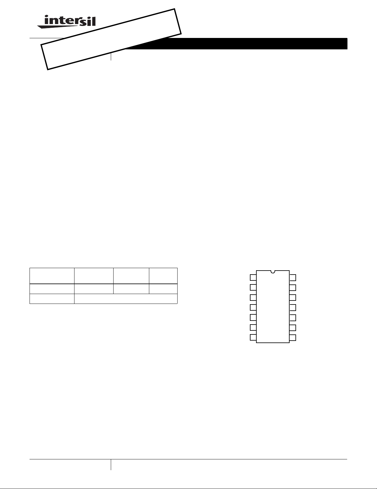
The HIP6602 is a high frequency, two power channel
MOSFET driver specifically designed to drive four power
N-Channel MOSFETs in a synchronous-rectified buck
converter topology. These drivers combined with a HIP63xx
series of Multi-Phase Buck PWM controller and Intersil’s
UltraFETs® form a complete core voltage regulator solution
for advanced microprocessors.
The HIP6602 drives both upper and lower gates over a
range of 5V to 12V. This drive-voltage flexibility provides the
advantage of optimizing applications involving trade-offs
between switching losses and conduction losses.
The output drivers in the HIP6602 have the capacity to
efficiently switch power MOSFETs at high frequencies. Each
driver is capable of driving a 3000pF load with a 30ns
propagation delay and 50ns transition time. This device
implements bootstrapping on the upper gates with only a
single external capacitor required for each power channel.
This reduces implementation complexity and allows the use
of higher performance, cost effective, N-Channel MOSFETs.
Adaptive shoot-through protection is integrated to prevent
both MOSFETs from conducting simultaneously.
Ordering Information
Features
• Drives Four N-channel MOSFETs
• Adaptive Shoot-Through Protection
• Internal Bootstrap Devices
• Supports High Switching Frequency
- Fast Output Rise Time
- Propagation Delay 30ns
• Small 14-Lead SOIC Package
• 5V to 12V Gate-Drive Voltages for Optimal Efficiency
• Three-State Input for Bridge Shutdown
• Supply Under-Voltage Protection
Applications
• Core Voltage Supplies for Intel Pentium® III and AMD®
AthlonTM Microprocessors.
• High Frequency Low Profile DC/DC Converters
• High Current Low Voltage DC/DC Converters
Pinout
HIP6602CB
(SOIC)
TOP VIEW
PART NUMBER
HIP6602CB 0 to 85 14 Ld SOIC M14.15
HIP6602CB-T 14 Ld SOIC Tape and Reel
TEMP. RANGE
(°C) PACKAGE PKG. NO.
PWM1
PWM2
GND
LGATE1
PVCC
PGND
LGATE2
1
1
2
2
3
4
5
6
14
13
12
11
10
9
87
VCC
PHASE1
UGATE1
BOOT1
BOOT2
UGATE2
PHASE2
1
Pentium
® is a registered trademark of Intel Corporation.; AMD® is a registered trademark of Advanced Micro Devices, Inc.
CAUTION: These devices are sensitive to electrostatic discharge; follow proper IC Handling Procedures.
UltraFET® is a registered trademark of Intersil Corporation. Athlon™ is a trademark of Advanced Micro Devices, Inc.
1-888-INTERSIL or 1-888-468-3774
| Copyright © Intersil Corporation 2000, 2005
Page 2
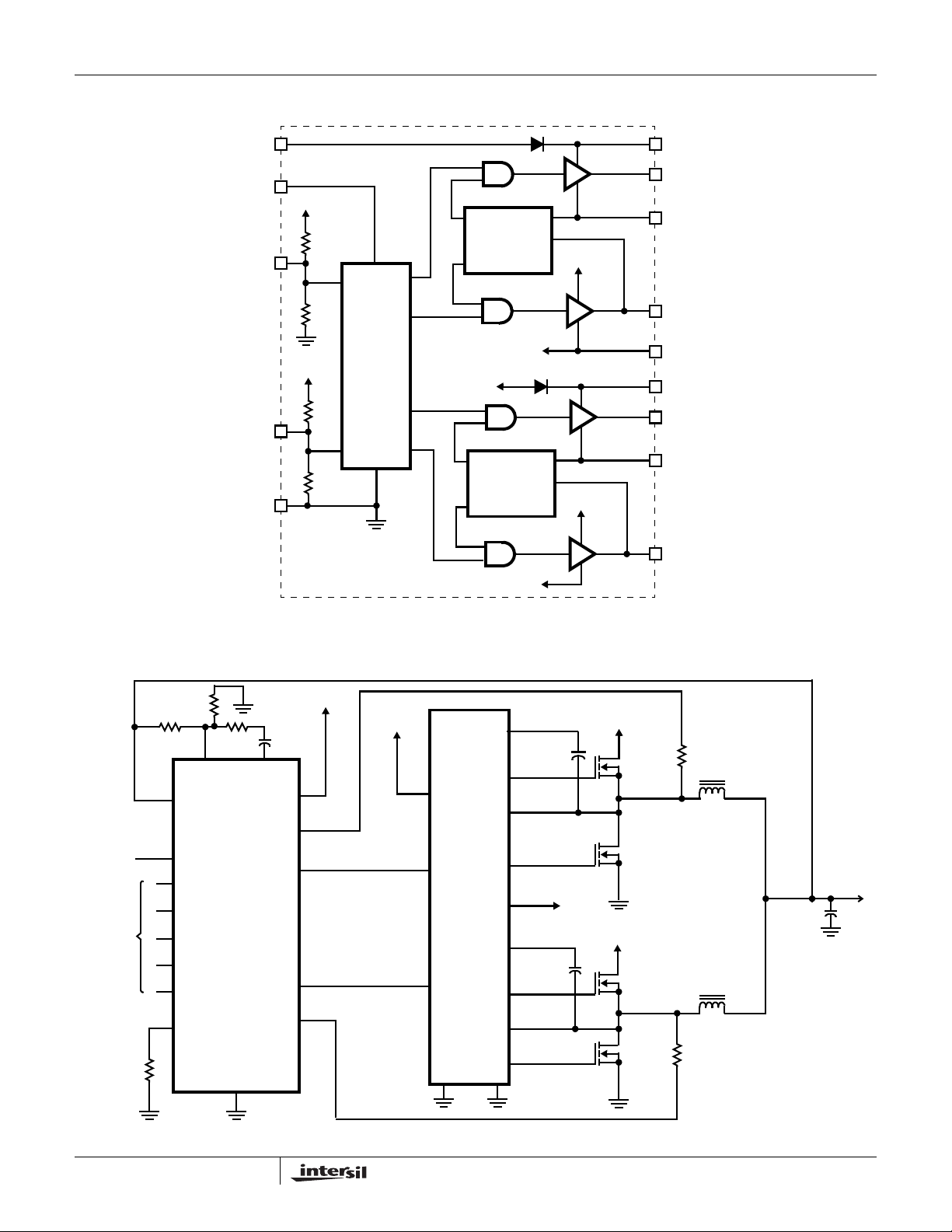
Block Diagram
HIP6602
PVCC
VCC
PWM1
PWM2
GND
+5V
10K
10K
+5V
10K
10K
HIP6602
CONTROL
LOGIC
SHOOT-
THROUGH
PROTECTION
PGND
PVCC
SHOOT-
THROUGH
PROTECTION
PGND
BOOT1
UGATE1
PHASE1
PVCC
LGATE1
PGND
BOOT2
UGATE2
PHASE2
PVCC
LGATE2
Typical Application - 2 Channel Converter Using a HIP6302 and a HIP6602 Gate Driver
+5V
BOOT1
UGATE1
PHASE1
LGATE1
PVCC
BOOT2
UGATE2
PHASE2
LGATE2
PGND
+12V
+V
+5V/12V
+12V
PGOOD
VID
FB
VSEN
FS/DIS
COMP
MAIN
CONTROL
HIP6302
GND
V
CC
ISEN1
PWM1
PWM2
ISEN2
+12V
VCC
PWM1
DUAL
DRIVER
HIP6602
PWM2
GND
CORE
2
Page 3
HIP6602
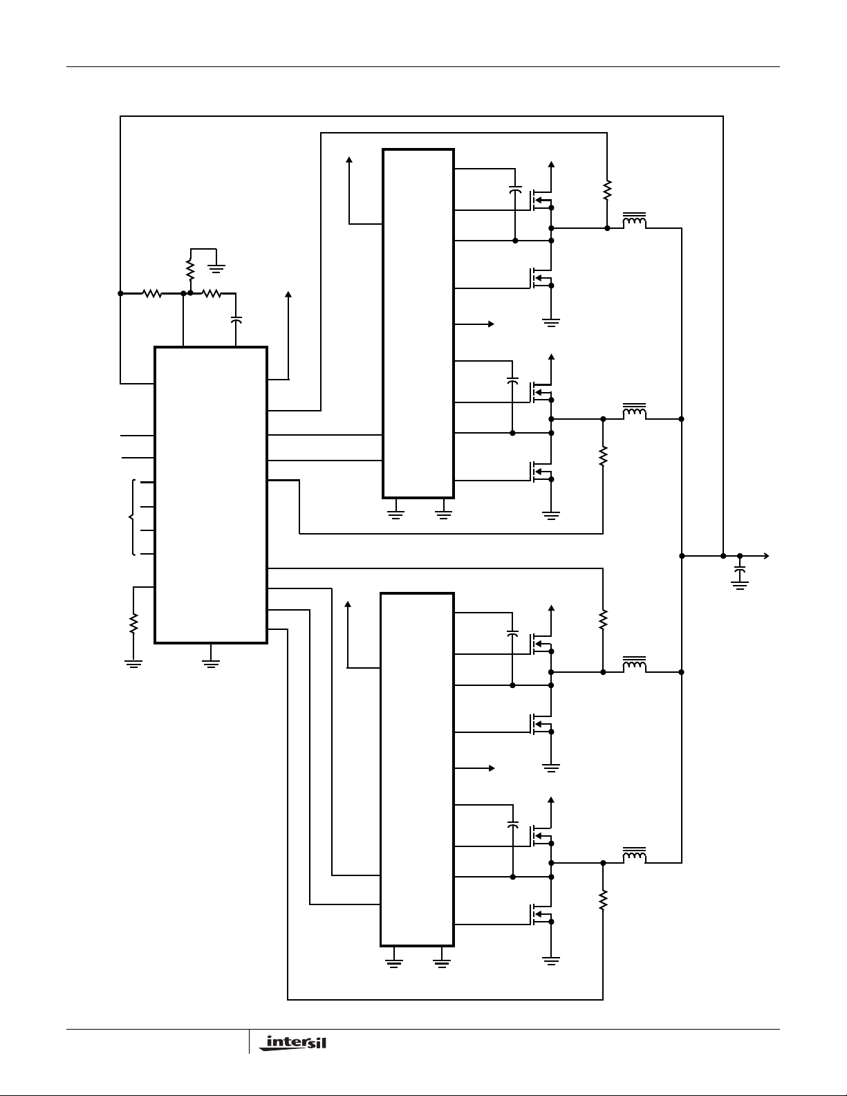
Typical Application - 4 Channel Converter Using a HIP6303 and HIP6602 Gate Driver
PGOOD
EN
VID
FB
VSEN
FS/DIS
COMP
MAIN
CONTROL
HIP6303
GND
V
CC
ISEN1
PWM1
PWM2
ISEN2
ISEN3
PWM3
PWM4
ISEN4
+5V
+12V
VCC
PWM1
PWM2
+12V
VCC
DUAL
DRIVER
HIP6602
BOOT1
UGATE1
PHASE1
LGATE1
PVCC
BOOT2
UGATE2
PHASE2
LGATE2
PGNDGND
BOOT3
UGATE3
PHASE3
+5V/12V
+12V
+12V
+12V
+V
CORE
LGATE3
DUAL
DRIVER
PVCC
+5V/12V
HIP6602
PWM3
PWM4
BOOT4
UGATE4
PHASE4
LGATE4
PGNDGND
+12V
3
Page 4
HIP6602
Absolute Maximum Ratings Thermal Information
Supply Voltage (VCC) . . . . . . . . . . . . . . . . . . . . . . . . . . . . . . . . .15V
Supply Voltage (PVCC) . . . . . . . . . . . . . . . . . . . . . . . . . VCC + 0.3V
BOOT Voltage (V
BOOT
- V
) . . . . . . . . . . . . . . . . . . . . . . .15V
PHASE
Input Voltage (VPWM). . . . . . . . . . . . . . . . . . . . . .GND - 0.3V to 7V
UGATE. . . . . . . . . . . . . . . . . . . . . .V
LGATE. . . . . . . . . . . . . . . . . . . . . . . . .GND - 0.3V to V
PHASE
- 0.3V to V
BOOT
PVCC
+ 0.3V
+ 0.3V
ESD Rating
Human Body Model (Per MIL-STD-883 Method 3015.7) . . . . .3kV
Machine Model (Per EIAJ ED-4701 Method C-111) . . . . . . .200V
Operating Conditions
Ambient Temperature Range. . . . . . . . . . . . . . . . . . . . . 0°C to 85°C
Maximum Operating Junction Temperature. . . . . . . . . . . . . . .125°C
Supply Voltage, VCC. . . . . . . . . . . . . . . . . . . . . . . . . . . . 12V ±10%
Supply Voltage Range PVCC . . . . . . . . . . . . . . . . . . . . . 5V to 12V
CAUTION: Stresses above those listed in “Absolute Maximum Ratings” may cause permanent damage to the device. This is a stress only rating and operation of the
device at these or any other conditions above those indicated in the operational sections of this specification is not implied.
NOTE:
is measured with the component mounted on a high effective thermal conductivity test board in free air. See Tech Brief TB379 for details.
1. θ
JA
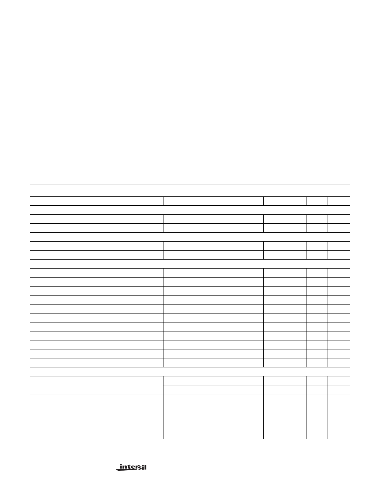
Electrical Specifications Recommended Operating Conditions, Unless Otherwise Noted
PARAMETER SYMBOL TEST CONDITIONS MIN TYP MAX UNITS
VCC SUPPLY CURRENT
Bias Supply Current I
Power Supply Current I
VCC
PVCC
POWER-ON RESET
VCC Rising Threshold 9.7 9.95 10.4 V
VCC Falling Threshold 9.0 9.2 9.5 V
PWM INPUT
Input Current I
PWM
PWM Rising Threshold V
PWM Falling Threshold V
UGATE Rise Time TR
LGATE Rise Time TR
UGATE Fall Time TF
LGATE Fall Time TF
UGATE Turn-Off Propagation Delay TPDL
LGATE Turn-Off Propagation Delay TPDL
UGATEVPVCC
LGATEVPVCC
UGATEVPVCC
LGATEVPVCC
UGATEVPVCC
LGATEVPVCC
Shutdown Window 1.4 - 3.6 V
Shutdown Holdoff Time - 230 - ns
OUTPUT
Upper Drive Source Impedance R
Upper Drive Sink Impedance R
Lower Drive Source Current I
Lower Drive Sink Impedance R
UGATEVVCC
UGATEVVCC
LGATE
LGATE
f
= 500kHz, V
PWM
f
= 500kHz, V
PWM
V
= 0 or 5V (See Block Diagram) - 500 - µA
PWM
= 12V 3.45 3.6 - V
PVCC
= 12V - 1.45 1.55 V
PVCC
= V
= V
= V
= V
= V
= V
= 12V, V
V
= V
VCC
= 12V, V
= V
V
VCC
V
= 12V, V
VCC
V
= V
VCC
V
= 12V, V
VCC
Thermal Resistance (Note 1) θ
SOIC Package . . . . . . . . . . . . . . . . . . . . . . . . . . . . . 68
Maximum Junction Temperature (Plastic Package) . . . . . . . .150°C
Maximum Storage Temperature Range . . . . . . . . . .-65°C to 150°C
Maximum Lead Temperature (Soldering 10s). . . . . . . . . . . . .300°C
(SOIC - Lead Tips Only)
= 12V - 3.7 5.0 mA
PVCC
= 12V - 2.0 4.0 mA
PVCC
= 12V, 3nF Load - 20 - ns
VCC
= 12V, 3nF Load - 50 - ns
VCC
= 12V, 3nF Load - 20 - ns
VCC
= 12V, 3nF Load - 20 - ns
VCC
= 12V, 3nF Load - 30 - ns
VCC
= 12V, 3nF Load - 20 - ns
VCC
= 5V - 1.7 3.0 Ω
PVCC
= 12V - 3.0 5.0 Ω
PVCC
= 5V - 2.3 4.0 Ω
PVCC
= 12V - 1.1 2.0 Ω
PVCC
= 5V 400 580 - mA
PVCC
= 12V 500 730 - mA
PVCC
= 5V or 12V - 1.6 4.0 Ω
PVCC
(°C/W)
JA
4
Page 5
HIP6602
Functional Pin Descriptions
PWM1 (Pin 1) and PWM2 (Pin 2)
The PWM signal is the control input for the driver. The PWM
signal can enter three distinct states during operation, see the
three-state PWM Input section under DESCRIPTION for further
details. Connect this pin to the PWM output of the controller.
GND (Pin 3)
Bias and reference ground. All signals are referenced to this
node.
LGATE1 (Pin 4) and LGATE2 (Pin 7)
Lower gate drive outputs. Connect to gates of the low-side
power N-Channel MOSFETs.
PVCC (Pin 5)
This pin supplies the upper and lower gate drivers bias.
Connect this pin from +12V down to +5V.
PGND (Pin 6)
This pin is the power ground return for the lower gate
drivers.
PHASE2 (Pin 8) and PHASE1 (Pin 13)
Connect these pins to the source of the upper MOSFETs
and the drain of the lower MOSFETs. The PHASE voltage is
monitored for adaptive shoot-through protection. These pins
also provide a return path for the upper gate drive.
UGATE2 (Pin 9) and UGATE1 (Pin 12)
Upper gate drive outputs. Connect to gate of high-side
power N-Channel MOSFETs.
BOOT 2 (Pin 10) and BOOT 1 (Pin 11)
Floating bootstrap supply pins for the upper gate drivers.
Connect the bootstrap capacitor between these pins and the
PHASE pin. The bootstrap capacitor provides the charge to
turn on the upper MOSFETs. See the Internal Bootstrap
Device section under DESCRIPTION for guidance in
choosing the appropriate capacitor value.
VCC (Pin 14)
Connect this pin to a +12V bias supply. Place a high quality
bypass capacitor from this pin to GND. To prevent forward
biasing an internal diode, this pin should be more positive
then PVCC during converter start-up.
Description
Operation
Designed for versatility and speed, the HIP6602 two channel,
dual MOSFET driver controls both high-side and low-side
N-Channel FETs from two externally provided PWM signals.
The upper and lower gates are held low until the driver is
initialized. Once the VCC voltage surpasses the VCC Rising
Threshold (See Electrical Specifications), the PWM signal
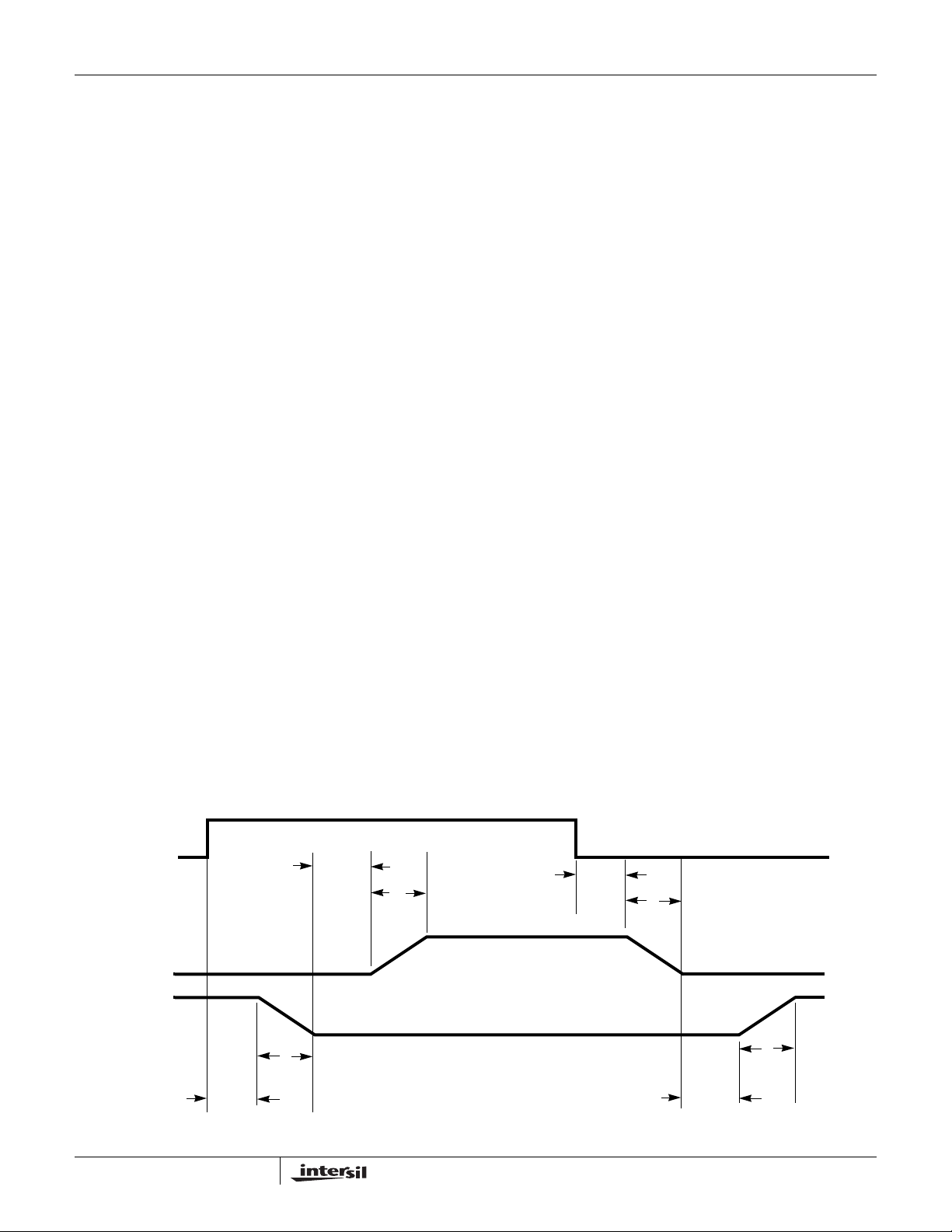
takes control of gate transitions. A rising edge on PWM
initiates the turn-off of the lower MOSFET (see Timing
Diagram). After a short propagation delay [TPDL
lower gate begins to fall. Typical fall times [TF
LGATE
provided in the Electrical Specifications section. Adaptive
shoot-through circuitry monitors the LGATE voltage and
determines the upper gate delay time [TPDH
UGATE
on how quickly the LGATE voltage drops below 1.0V. This
prevents both the lower and upper MOSFETs from
conducting simultaneously or shoot-through. Once this delay
period is complete the upper gate drive begins to rise
[TR
] and the upper MOSFET turns on.
UGATE
LGATE
] are
] based
], the
Timing Diagram
PWM
UGATE
LGATE
TPDL
LGATE
TPDH
UGATE
TF
LGATE
5
TR
UGATE
TPDL
UGATE
TPDH
TF
UGATE
LGATE
TR
LGATE
Page 6

HIP6602
A falling transition on PWM indicates the turn-off of the
upper MOSFET and the turn-on of the lower MOSFET. A
short propagation delay [TPDL
before the upper gate begins to fall [TF
] is encountered
UGATE
UGATE
]. Again, the
adaptive shoot-through circuitry determines the lower gate
delay time, TPDH
. The PHASE voltage is monitored
LGATE
and the lower gate is allowed to rise after PHASE drops
below 0.5V. The lower gate then rises [TR
LGATE
], turning
on the lower MOSFET.
Three-State PWM Input
A unique feature of the HIP6602 drivers is the addition of a
shutdown window to the PWM input. If the PWM signal
enters and remains within the shutdown window for a set
holdoff time, the output drivers are disabled and both
MOSFET gates are pulled and held low. The shutdown state
is removed when the PWM signal moves outside the
shutdown window. Otherwise, the PWM rising and falling
thresholds outlined in the ELECTRICAL SPECIFICATIONS
determine when the lower and upper gates are enabled.
Adaptive Shoot-Through Protection
The drivers incorporate adaptive shoot-through protection to
prevent upper and lower MOSFETs from conducting
simultaneously and shorting the input supply. This is
accomplished by ensuring the falling gate has turned off one
MOSFET before the other is allowed to rise.
During turn-off of the lower MOSFET, the LGATE voltage is
monitored until it reaches a 1.0V threshold, at which time the
UGATE is released to rise. Adaptive shoot-through circuitry
monitors the PHASE voltage during UGATE turn-off. Once
PHASE has dropped below a threshold of 0.5V, the LGATE
is allowed to rise. If the PHASE does not drop below 0.5V
within 250ns, LGATE is allowed to rise. This is done to
generate the bootstrap refresh signal. PHASE continues to
be monitored during the lower gate rise time. If the PHASE
voltage exceeds the 0.5V threshold during this period and
remains high for longer than 2µs, the LGATE transitions low.
This is done to make the lower MOSFET emulate a diode.
Both upper and lower gates are then held low until the next
rising edge of the PWM signal.
Power-On Reset (POR) Function
During initial start-up, the VCC voltage rise is monitored and
gate drives are held low until a typical VCC rising threshold
of 9.95V is reached. Once the rising VCC threshold is
exceeded, the PWM input signal takes control of the gate
drives. If VCC drops below a typical VCC falling threshold of
9.2V during operation, then both gate drives are again held
low. This condition persists until the VCC voltage exceeds
the VCC rising threshold.
Internal Bootstrap Device
Both drivers feature an internal bootstrap device. Simply
adding an external capacitor across the BOOT and PHASE
pins completes the bootstrap circuit.
The bootstrap capacitor must have a maximum voltage
rating above PVCC + 5V. The bootstrap capacitor can be
chosen from the following equation:
Q
C
BOOT
Where Q
charge the gate of the upper MOSFET. The ∆V
GATE
------------------------≥
∆V
BOOT
is the amount of gate charge required to fully
GATE
BOOT
term is
defined as the allowable droop in the rail of the upper drive.
As an example, suppose a HUF76139 is chosen as the
upper MOSFET. The gate charge, Q
, from the data
GATE
sheet is 65nC for a 10V upper gate drive. We will assume a
200mV droop in drive voltage over the PWM cycle. We find
that a bootstrap capacitance of at least 0.325µF is required.
The next larger standard value capacitance is 0.33µF.
Gate Drive Voltage Versatility
The HIP6602 provides the user flexibility in choosing the
gate drive voltage. Simply applying a voltage from 5V up to
12V on PVCC will set both driver rail voltages.
Power Dissipation
Package power dissipation is mainly a function of the switching
frequency and total gate charge of the selected MOSFETs.
Calculating the power dissipation in the driver for a desired
application is critical to ensuring safe operation. Exceeding the
maximum allowable power dissipation level will push the IC
beyond the maximum recommended operating junction
temperature of 125°C. The maximum allowable IC power
dissipation for the 14 lead SOIC package is approximately
1000mW. Improvements in thermal transfer may be gained by
increasing the PC board copper area around the HIP6602.
Adding a ground pad under the IC to help transfer heat to the
outer peripheral of the board will help. Also keeping the leads to
the IC as wide as possible and widening this these leads as
soon as possible to further enhance heat transfer will also help.
When designing the driver into an application, it is
recommended that the following calculation be performed to
ensure safe operation at the desired frequency for the
selected MOSFETs. The total chip power dissipation is
approximated as:
3
P = 1.05 x fSW x V
where f
and Q
is the switching frequency of the PWM signal. QU
sw
is the upper and lower gate charge determined by
L
MOSFET selection and any external capacitance added to
the gate pins. The I
of the driver and is typically 40mW.
The 1.05 term is a correction factor derived from the
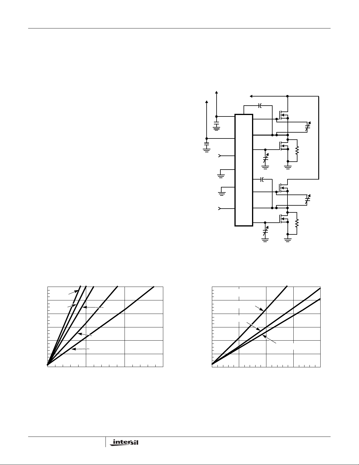
following characterization. The base circuit for characterizing
the drivers for different loading profiles and frequencies is
provided. C
and CL are the upper and lower gate load
U
capacitors. Decoupling capacitors [0.15µF] are added to the
_
[ (QU1 + QU2) + (QL1 + QL2)] + I
PVCC
2
VCC product is the quiescent power
DDQ
DDQ
x VCC
6
Page 7
HIP6602
PVCC and VCC pins. The bootstrap capacitor value in the
test circuit is 0.01µF.
The power dissipation approximation is a result of power
transferred to and from the upper and lower gates. But, the
internal bootstrap device also dissipates power on-chip
during the refresh cycle. Expressing this power in terms of
the upper MOSFET total gate charge is explained below.
The bootstrap device conducts when the lower MOSFET or
its body diode conducts and pulls the PHASE node toward
GND. While the bootstrap device conducts, a current path is
formed that refreshes the bootstrap capacitor. Since the
upper gate is driving a MOSFET, the charge removed from
the bootstrap capacitor is equivalent to the total gate charge
of the MOSFET. Therefore, the refresh power required by
the bootstrap capacitor is equivalent to the power used to
charge the gate capacitance of the upper MOSFETs.
P
REFRESHfSW
where Q
LOSS
Q
LOSS
V
PVCC
==
fSWQUV
PVCC
is the total charge removed from the bootstrap
capacitors and provided to the upper gate loads.
In Figure 1, C
and CL values are the same and frequency
U
is varied from 10kHz to 2MHz. PVCC and VCC are tied
together to a +12V supply.
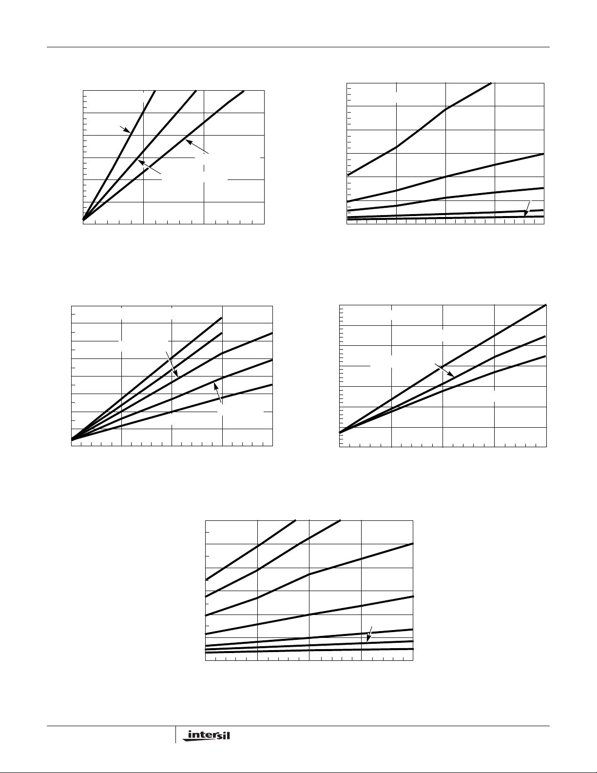
tied together and to a +12V supply. Figures 5 through 7
show the same characterization for PVCC tied to +5V
instead of +12V. The gate supply voltage, PVCC, within the
HIP6602 sets both upper and lower gate driver supplies at
the same 5V level for the last three curves.
Test Circuit
+5V OR +12V
0.15µF
0.15µF
+5V OR +12V
PVCC
VCC
PWM1
PGND
GND
PWM2
0.01µF
BOOT1
HIP6602
UGATE1
PHASE1
LGATE1
0.01µF
BOOT2
UGATE2
PHASE2
2N7002
C
L
2N7002
2N7002
100kΩ
C
U
C
U
+12V
Figure 2 shows the dissipation in the driver with 1nF loading
on both gates and each individually. Figure 3 is the same as
Figure 2 except the capacitance is increased to 3nF.
The impact of loading on power dissipation is shown in
Figure 4. Frequency is held constant while the gate
capacitors are varied from 1nF to 5nF. VCC and PVCC are
Typical Performance Curves
1200
CU = C
L
= 5nF
CU = C
L
= 4nF
0
0 500 1000 1500
FREQUENCY (kHz)
C
= CL = 2nF
U
C
= CL = 1nF
U
C
= C
U
= 3nF
L
PVCC = 12V
VCC = 12V
POWER (mW)
1000
800
600
400
200
LGATE2
2N7002
C
L
1200
PVCC = VCC = 12V
POWER (mW)
1000
800
600
400
200
0
C
= CL = 1nF
U
CL = 1nF, CU = 0nF
CU = 1nF, CL = 0nF
0 500 1000 2000
FREQUENCY (kHz)
1500
100kΩ
FIGURE 1. POWER DISSIPATION vs FREQUENCY FIGURE 2. 1nF LOADING PROFILE
7
Page 8
Typical Performance Curves (Continued)
HIP6602
1200
PVCC = VCC = 12V
1000
C
= CL = 3nF
U
800
600
POWER (mW)
400
200
0
0 500 1000
FREQUENCY (kHz)
FIGURE 3. 3nF LOADING PROFILE FIGURE 4. POWER DISSIPATION vs LOADING
800
700
600
500
400
300
POWER (mW)
200
100
PVCC = 5V, VCC = 12V
CU = CL = 3nF
CU = 3nF, CL = 0nF
CL = 3nF, CU = 0nF
CU = CL =1nF
CU = CL = 5nF
CU = CL = 4nF
CU = CL = 2nF
1500
1200
PVCC = VCC = 12V
1000
500kHz
800
600
POWER (mW)
400
200
0
12345
GATE CAPACITANCE (CU = CL), (nF)
350
300
250
200
150
POWER (mW)
100
50
PVCC = 5V, VCC = 12V
CL = 1nF, CU = 0nF
200kHz
100kHz
30kHz
CU = CL = 1nF
CU = 1nF, CL = 0nF
10kHz
0
0 500 1500 2000
1000
FREQUENCY (kHz)
0
0 500 1000 1500 2000
FREQUENCY (kHz)
FIGURE 5. POWER DISSIPATION vs FREQUENCY, PVCC = 5V FIGURE 6. POWER DISSIPATION vs FREQUENCY, PVCC = 5V
600
PVCC = 5V,
VCC = 12V
POWER (mW)
500
2MHz
400
300
200
100
0
1.5MHz
500kHz
GATE CAPACITANCE (C
1MHz
200kHz
= CL), (nF)
U
100kHz
30kHz
54321
FIGURE 7. POWER DISSIPATION vs LOADING, PVCC = 5V
8
Page 9
Small Outline Plastic Packages (SOIC)
HIP6602
N
INDEX
AREA
123
-A-
E
-B-
SEATING PLANE
D
A
-C-
0.25(0.010) BM M
H
L
h x 45
o
α
e
B
0.25(0.010) C AM BS
M
NOTES:
1. Symbols are defined in the “MO Series Symbol List” in Section 2.2 of
Publication Number 95.
2. Dimensioning and tolerancing per ANSI Y14.5M-1982.
3. Dimension “D” does not include mold flash, protrusions or gate burrs.
Mold flash, protrusion and gate burrs shall not exceed 0.15mm (0.006
inch) per side.
4. Dimension “E” does not include interlead flash or protrusions. Interlead
flash and protrusions shall not exceed 0.25mm (0.010 inch) per side.
5. The chamfer on the body is optional. If it is not present, a visual index
feature must be located within the crosshatched area.
6. “L” is the length of terminal for soldering to a substrate.
7. “N” is the number of terminal positions.
8. Terminal numbers are shown for reference only.
9. The lead width “B”, as measured 0.36mm (0.014 inch) or greater
above the seating plane, shall not exceed a maximum value of
0.61mm (0.024 inch).
10. Controlling dimension: MILLIMETER. Converted inch dimensions
are not necessarily exact.
A1
C
0.10(0.004)
M14.15 (JEDEC MS-012-AB ISSUE C)
14 LEAD NARROW BODY SMALL OUTLINE PLASTIC
PACKAGE
INCHES MILLIMETERS
SYMBOL
A 0.0532 0.0688 1.35 1.75 -
A1 0.0040 0.0098 0.10 0.25 -
B 0.013 0.020 0.33 0.51 9
C 0.0075 0.0098 0.19 0.25 D 0.3367 0.3444 8.55 8.75 3
E 0.1497 0.1574 3.80 4.00 4
e 0.050 BSC 1.27 BSC H 0.2284 0.2440 5.80 6.20 -
h 0.0099 0.0196 0.25 0.50 5
L 0.016 0.050 0.40 1.27 6
N14 147
o
α
0
o
8
o
0
o
8
Rev. 0 12/93
NOTESMIN MAX MIN MAX
-
All Intersil semiconductor products are manufactured, assembled and tested under ISO9000 quality systems certification.
Intersil semiconductor products are sold b y de scr ip tion on ly. Intersil Corporation reserves the right to make changes in circuit design and/or specifications at any time without notice. Accordingly, the reader is cautioned to verify that data sheets are current before placing orders. Information furnished by Intersil is believed to be accurate and
reliable. However, no responsibility is assumed by Intersil or its subsidiaries for its use; nor for any infringements of patents or other rights of third parties which may result
from its use. No license is granted by implication or othe rwise under any patent or patent rights of Intersil or its subsidiaries.
For information regarding Intersil Corporation and its products, see web site www.intersil.com
9
 Loading...