

Page 1
查询HIP6013供应商
HIP6013
Data Sheet June 1997
Buck Pulse-Width Modulator (PWM)
Controller
The HIP6013 provides complete control and protection for a
DC-DC converter optimized for high-performance
microprocessor applications. It is designed to drive an
N-Channel MOSFET in a standard buck topology. The
HIP6013 integrates all of the control, output adjustment,
monitoring and protection functions into a single package.
The output voltage of the converter can be precisely
regulated to as low as 1.27V, with a maximum tolerance of
±1.5% over temperature and line voltage variations.
The HIP6013 provides simple,single feedback loop, voltagemode control with fast transient response. It includes a
200kHz free-running triangle-wave oscillator that is
adjustable from below 50kHz to over 1MHz. The error
amplifier features a 15MHz gain-bandwidth product and
6V/µs slew rate which enables high converter bandwidth for
fast transient performance. The resulting PWM duty ratio
ranges from 0% to 100%.
The HIP6013 protects against over-current conditions by
inhibiting PWM operation. The HIP6013 monitors the current
by using the r
DS(ON)
the need for a current sensing resistor.
of the upper MOSFET which eliminates
File Number
Features
• Drives N-Channel MOSFET
• Operates From +5V or +12V Input
• Simple Single-Loop Control Design
- Voltage-Mode PWM Control
• Fast Transient Response
- High-Bandwidth Error Amplifier
- Full 0% to 100% Duty Ratio
• Excellent Output Voltage Regulation
- 1.27V Internal Reference
- ±1.5% Over Line Voltage and Temperature
• Over-Current Fault Monitor
- Does Not Require Extra Current Sensing Element
- Uses MOSFET’s r
DS(on)
• Small Converter Size
- Constant Frequency Operation
- 200kHz Free-Running Oscillator Programmable from
50kHz to Over 1MHz
• 14 Pin, SOIC Package
Applications
4325
Ordering Information
TEMP.RANGE
PART NUMBER
HIP6013CB 0 to 70 14 Ld SOIC M14.15
(oC) PACKAGE
PKG.
NO.
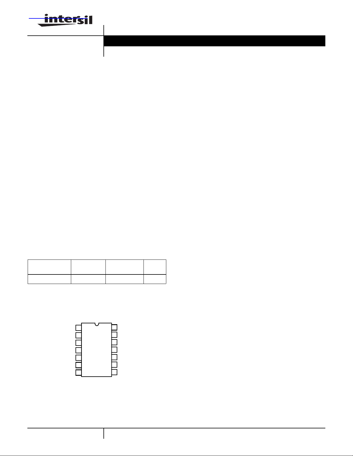
Pinout
HIP6013
(SOIC)
TOP VIEW
RT
OCSET
SS
COMP
FB
EN
GND
1
2
3
4
5
6
7
14
13
12
11
10
9
8
VCC
NC
NC
NC
BOOT
UGATE
PHASE
• Power Supply for Pentium®, Pentium Pro, PowerPC™and
Alpha™ Microprocessors
• High-Power 5V to 3.xV DC-DC Regulators
• Low-Voltage Distributed Power Supplies
PowerPC™ is a trademark of IBM.
Alpha™ is a trademark of Digital Equipment Corporation.
Pentium® is a registered trademark of Intel Corporation.
2-162
CAUTION: These devices are sensitive to electrostatic discharge; follow proper IC Handling Procedures.
http://www.intersil.com or 407-727-9207
| Copyright © Intersil Corporation 1999
Page 2
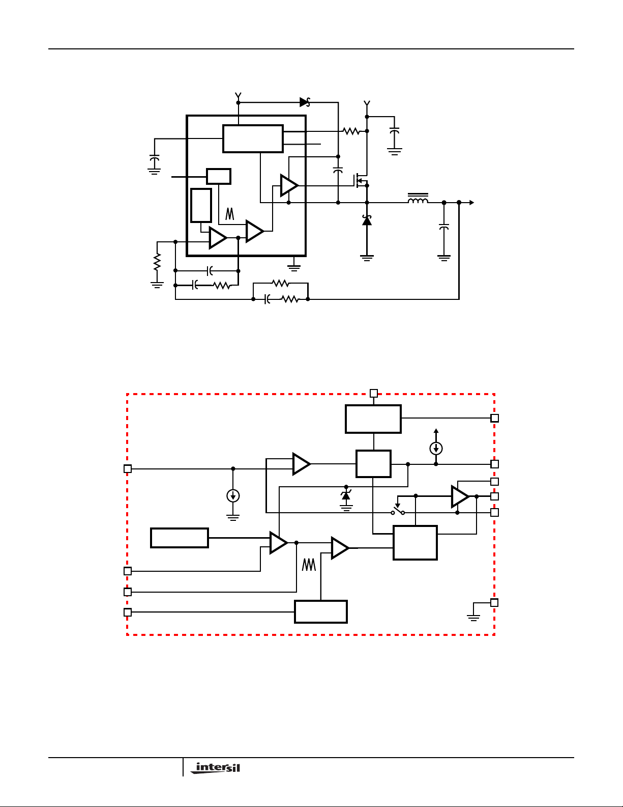
Typical Application
12V
VCC
HIP6013
+5V OR +12V
Block Diagram
SS
RT
FB
REF
MONITOR AND
PROTECTION
OSC
HIP6013
+
-
COMP
OCSET
EN
BOOT
UGATE
+V
PHASE
+
VCC
POWER-ON
RESET (POR)
O
EN
OCSET
FB
COMP
RT
REFERENCE
200µA
1.27 VREF
+
-
ERROR
AMP
+
-
OVER-
CURRENT
4V
PWM
COMPARATOR
OSCILLATOR
10µA
SOFT-
START
+
-
INHIBIT
PWM
GATE
CONTROL
LOGIC
SS
BOOT
UGATE
PHASE
GND
2-163
Page 3
HIP6013
Absolute Maximum Ratings Thermal Information
Supply Voltage, VCC . . . . . . . . . . . . . . . . . . . . . . . . . . . . . . . +15.0V
Boot Voltage, V
BOOT
- V
. . . . . . . . . . . . . . . . . . . . . . . +15.0V
PHASE
Input, Output or I/O Voltage. . . . . . . . . . . GND -0.3V to VCC +0.3V
ESD Classification . . . . . . . . . . . . . . . . . . . . . . . . . . . . . . . . .Class 2
Operating Conditions
Supply Voltage, VCC . . . . . . . . . . . . . . . . . . . . . . . . . . . +12V ±10%
Ambient Temperature Range. . . . . . . . . . . . . . . . . . . . .0oC to 70oC
Junction Temperature Range. . . . . . . . . . . . . . . . . . . . 0oC to 125oC
CAUTION: Stresses above those listed in “Absolute Maximum Ratings” may cause permanent damage to the device. This is a stress only rating and operationofthe
device at these or any other conditions above those indicated in the operational sections of this specification is not implied.
NOTE:
1. θJA is measured with the component mounted on an evaluation PC board in free air.
Electrical Specifications Recommended Operating Conditions, Unless Otherwise Noted
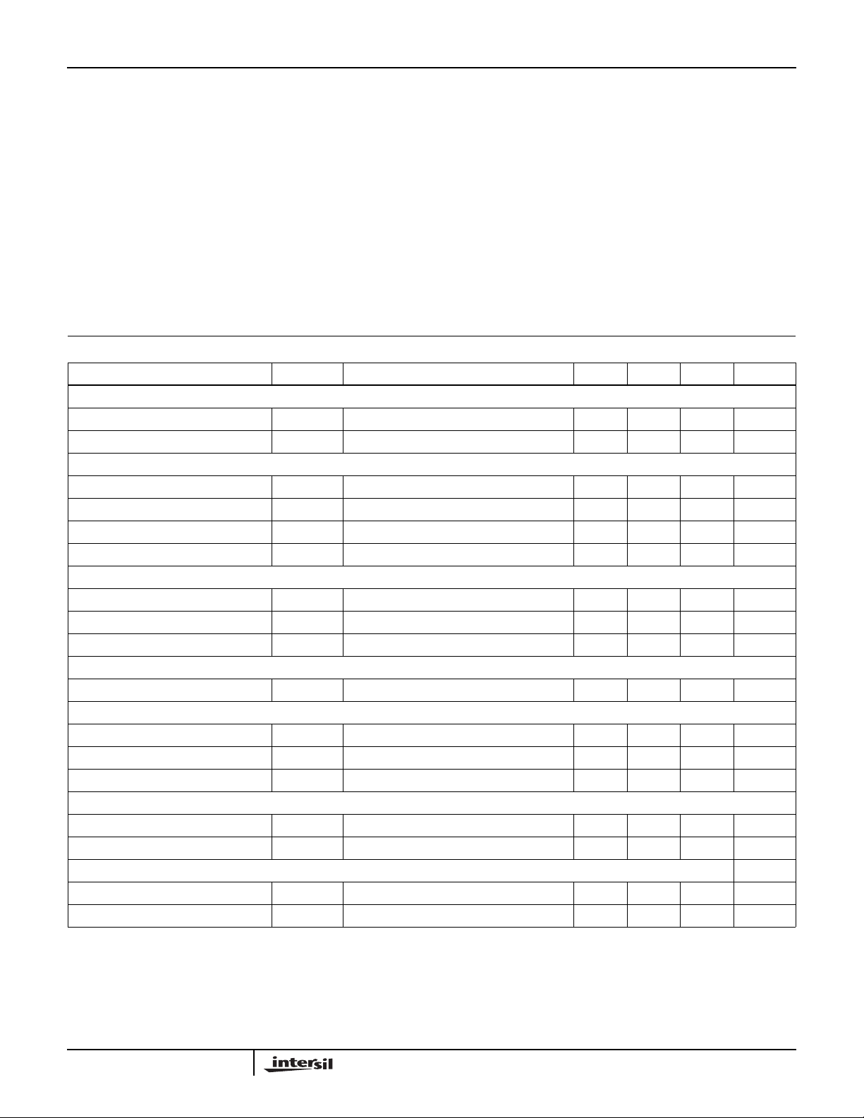
PARAMETER SYMBOL TEST CONDITIONS MIN TYP MAX UNITS
VCC SUPPLY CURRENT
Nominal Supply I
CC
Shutdown Supply EN = 0V - 50 100 µA
POWER-ON RESET
Rising VCC Threshold V
Falling VCC Threshold V
Enable - Input threshold Voltage V
Rising V
Threshold - 1.27 - V
OCSET
OSCILLATOR
Free Running Frequency RT = OPEN, VCC= 12 180 200 220 kHz
Total Variation 6kΩ < RT to GND < 200kΩ -20 - +20 %
Ramp Amplitude ∆V
OSC
REFERENCE
Reference Voltage 1.251 1.270 1.289 V
ERROR AMPLIFIER
DC Gain -88- dB
Gain-Bandwidth Product GBW - 15 - MHz
Slew Rate SR COMP = 10pF - 6 - V/µs
GATE DRIVERS
Upper Gate Source I
Upper Gate Sink R
UGATE
UGATEILGATE
PROTECTION
OCSET Current Source I
Soft Start Current I
OCSETVOCSET
SS
EN = VCC; UGATE and LGATE Open - 5 - mA
= 4.5VDC - - 10.4 V
OCSET
= 4.5VDC 8.8 - - V
OCSET
= 4.5VDC 0.8 - 2.0 V
OCSET
RT = OPEN - 1.9 - V
V
- V
BOOT
PHASE
= 0.3A - 5.5 10 Ω
= 4.5VDC 170 200 230 µA
Thermal Resistance (Typical, Note 1) θJA (oC/W)
SOIC Package . . . . . . . . . . . . . . . . . . . . . . . . . . . . . 185
Maximum Junction Temperature . . . . . . . . . . . . . . . . . . . . . . 150oC
Maximum Storage Temperature Range. . . . . . . . . . -65oC to 150oC
Maximum Lead Temperature (Soldering 10s) . . . . . . . . . . . . 300oC
(SOIC - Lead Tips Only)
= 12V, V
= 6V 350 500 - mA
UGATE
-10- µA
P-P
2-164
Page 4
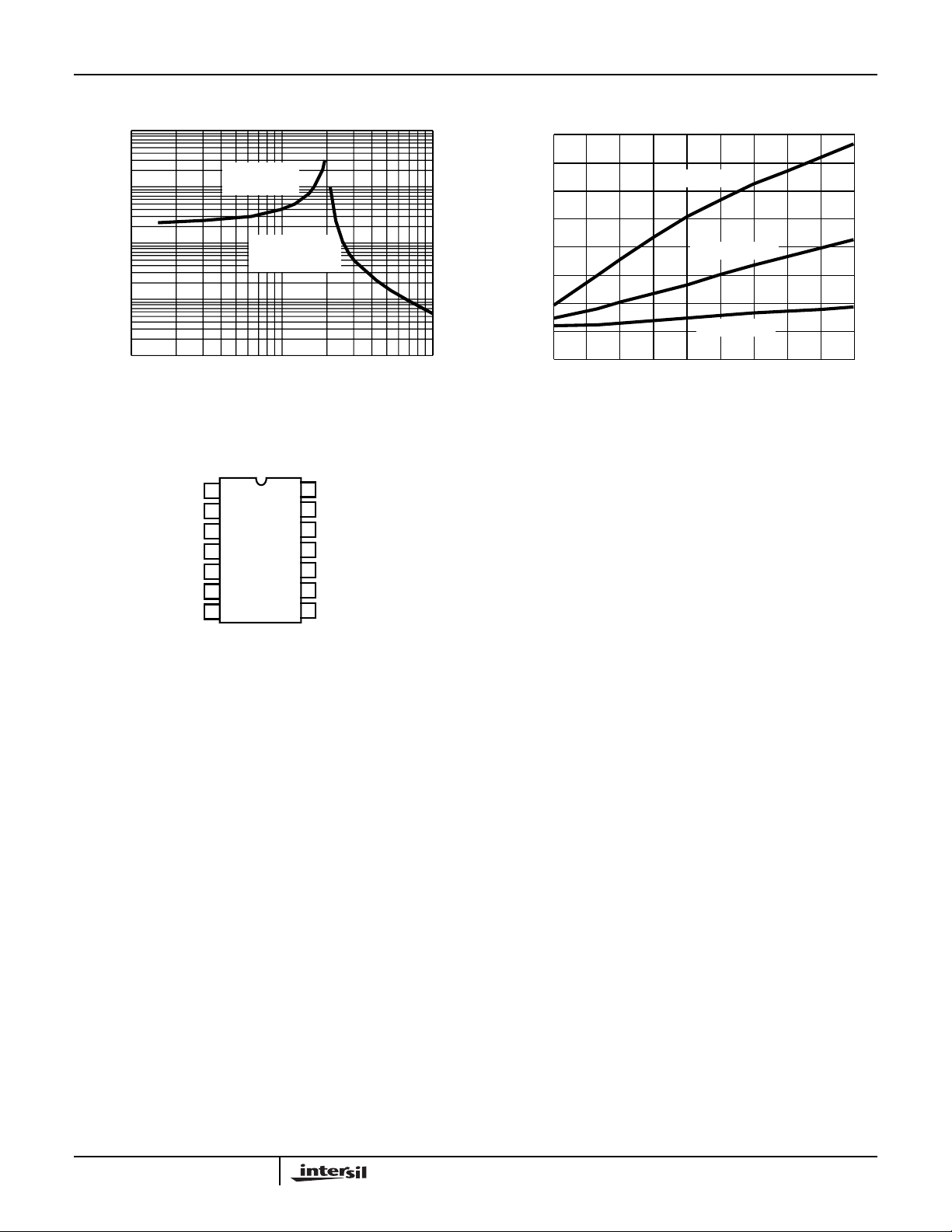
Typical Performance Curves
HIP6013
40
RT PULLUP
1000
100
RESISTANCE (kΩ)
10
10 100 1000
SWITCHING FREQUENCY (kHz)
FIGURE 1. RT RESISTANCE vs FREQUENCY FIGURE 2. BIAS SUPPLY CURRENT vs FREQUENCY
TO +12V
RT PULLDOWN
TO V
SS
Functional Pin Description
1
RT
OCSET
SS
COMP
FB
EN
GND
2
3
4
5
6
7
RT (Pin 1)
This pin provides oscillator switching frequency adjustment.
By placing a resistor (R
200kHz switching frequency is increased according to the
following equation:
510
Fs 200kHz
•
------------------+≈
R
Conversely, connecting a pull-up resistor (R
to VCC reduces the switching frequency according to the
following equation.:
410
Fs 200kHz
•
------------------–≈
R
) from this pin to GND, the nominal
T
6
T
T
(RT to GND)
7
(RT to 12V)
14
13
12
11
10
9
8
VCC
NC
NC
NC
BOOT
UGATE
PHASE
) from this pin
T
35
30
25
20
(mA)
CC
I
15
10
5
0
100 200 300 400 500 600 700 800 900 1000
C
= 3300pF
GATE
C
= 1000pF
GATE
C
= 10pF
GATE
SWITCHING FREQUENCY (kHz)
SS (Pin 3)
Connect a capacitor from this pin to ground. This capacitor,
along with an internal 10µA current source, sets the softstart interval of the converter.
COMP (Pin 4) and FB (Pin 5)
COMP and FB are the available external pins of the error
amplifier. The FB pin is the inverting input of the error
amplifier and the COMP pin is the error amplifier output.
These pins are used to compensate the voltage-control
feedback loop of the converter.
EN (Pin 6)
This pin is the open-collector enable pin. Pull this pin below
1V to disable the converter. In shutdown, the soft start pin is
discharged and the UGATE and LGATE pins are held low.
GND (Pin 7)
Signal ground for the IC.All voltage levelsare measured with
respect to this pin.
PHASE (Pin 8)
Connect the PHASE pin to the upper MOSFET source. This
pin is used to monitor the voltage drop across the MOSFET
for over-current protection. This pin also provides the return
path for the upper gate drive.
OCSET (Pin 2)
Connect a resistor (R
upper MOSFET. R
(I
), and the upper MOSFET on-resistance (r
OCS
OCSET
the converter over-current (OC) trip point according to the
following equation:
I
•
I
PEAK
OCSROCSET
------------------------------------------- -=
r
DS ON()
An over-current trip cycles the soft-start function.
) from this pin to the drain of the
OCSET
, an internal 200µA current source
DS(ON)
2-165
) set
UGATE (Pin 9)
Connect UGATE to the upper MOSFET gate. This pin
provides the gate drive for the upper MOSFET.
BOOT (Pin 10)
This pin provides bias voltage to the upper MOSFET driver.
A bootstrap circuit may be used to create a BOOT voltage
suitable to drive a standard N-Channel MOSFET.
VCC (Pin 14)
Provide a 12V bias supply for the chip to this pin.
Page 5
Functional Description
Initialization
The HIP6013 automatically initializes upon receipt of power.
Special sequencing of the input supplies is not necessary.
The Power-On Reset (POR) function continually monitors
the input supply voltages and the enable (EN) pin. The POR
monitors the bias voltage at the VCC pin and the input
voltage (V
equal to V
protection). With the EN pin held to VCC, the POR function
initiates soft start operation after both input supply voltages
exceed their POR thresholds. For operation with a single
+12V power source, V
+12V power source must exceed the rising V
before POR initiates operation.
The Power-On Reset (POR) function inhibits operation with
the chip disabled (EN pin low). With both input supplies
above their POR thresholds, transitioning the EN pin high
initiates a soft start interval.
Soft Start
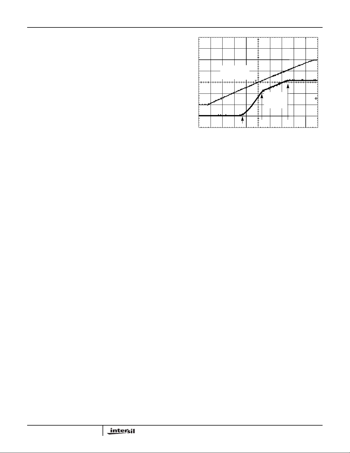
The POR function initiates the soft start sequence. An
internal 10µA current source charges an external capacitor
(C
SS
amplifier output (COMP pin) and reference input (+ terminal
of error amp) to the SS pin voltage. Figure 3 shows the soft
start interval with C
error amplifier (COMP pin) controls the converter’s output
voltage. At t1 in Figure 3, the SS voltage reaches the valley
of the oscillator’s triangle wave. The oscillator’s triangular
waveform is compared to the ramping error amplifier voltage.
This generates PHASE pulses of increasing width that
charge the output capacitor(s). This interval of increasing
pulse width continues to t2. With sufficient output voltage,
the clamp on the reference input controls the output voltage.
This is the interval between t2 and t3 in Figure 3. At t3 the
SS voltage exceeds the reference voltage and the output
voltage is in regulation. This method provides a rapid and
controlled output voltage rise.
) on the OCSET pin. The level on OCSET is
IN
less a fixed voltage drop (see over-current
IN
and VCC are equivalent and the
IN
threshold
CC
) on the SS pin to 4V. Soft start clamps the error
= 0.1µF. Initially the clamp on the
SS
HIP6013
SOFT-START
(1V/DIV)
OUTPUT
VOLTAGE
0V
0V
t1 t2 t3
TIME (5ms/DIV)
FIGURE 3. SOFT-START INTERVAL
(1V/DIV)
Over-Current Protection
The over-current function protects the converter from a
shorted output by using the upper MOSFET’s on-resistance,
r
converter’s efficiency and reduces cost by eliminating a
current sensing resistor.
The over-current function cycles the soft-start function in a
hiccup mode to provide fault protection. A resistor (R
programs the over-current trip level. An internal 200µA
(typical) current sink develops a voltage across R
is reference to V
MOSFET (also referenced to V
across R
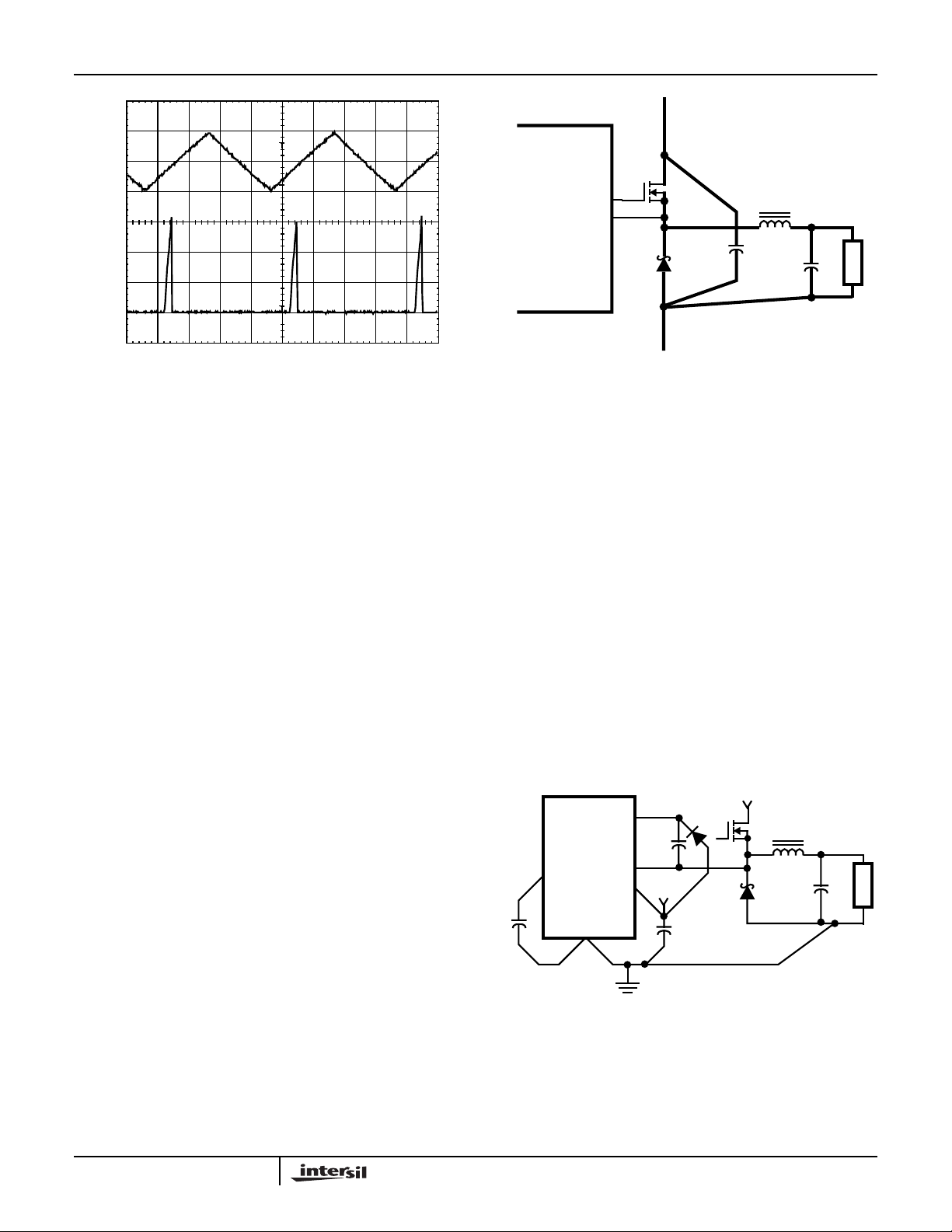
start sequence. The soft-start function discharges C
a 10µA current sink and inhibits PWM operation. The softstart function recharges C
with the error amplifier clamped to the SS voltage. Should an
overload occur while recharging C
inhibits PWM operation while fully charging C
complete its cycle. Figure 4 shows this operation with an
overload condition. Note that the inductor current increases
to over 15A during the C
over-current trip. The converter dissipates very little power
with this method. The measured input power for the
conditions of Figure 4 is 2.5W.
to monitor the current. This method enhances the
DS(ON)
. When the voltage across the upper
IN
, the over-current function initiates a soft-
OCSET
SS
) exceeds the voltage
IN
, and PWM operation resumes
SS
, the soft start function
SS
charging interval and causes an
OCSET
to 4V to
SS
OCSET
that
with
SS
)
2-166
Page 6
4V
HIP6013
V
IN
2V
SOFT-START
0V
15A
10A
5A
OUTPUT INDUCTOR
0A
TIME (20ms/DIV)
FIGURE 4. OVER-CURRENT OPERATION
The over-current function will trip at a peak inductor current
(I
) determined by:
PEAK
I
PEAK
where I
I
---------------------------------------------------=
OCSET
•
OCSETROCSET
r
DS ON()
is the internal OCSET current source (200µA
- typical). The OC trip point varies mainly due to the
MOSFET’sr
DS(ON)
in the normal operating load range, find the R
variations. To avoid over-current tripping
OCSET
resistor
from the equation above with:
1. Themaximumr
2. The minimum I
3. Determine ,
I
PEAK
DS(ON)
OCSET
atthehighest junction temperature.
from the specification table.
for I
PEAKIOUT MAX()
∆I()2⁄+>
where ∆I is the output inductor ripple current.
For an equation for the ripple current see the section under
component guidelines titled ‘Output Inductor Selection’.
A small ceramic capacitor should be placed in parallel with
R
to smooth the voltage across R
OCSET
OCSET
in the
presence of switching noise on the input voltage.
Application Guidelines
Layout Considerations
As in any high frequency switching conv erter , la y out is very
important. Switching current from one power device to another
can generate voltage transients across the impedances of the
interconnecting bond wires and circuit traces. These
interconnecting impedances should be minimized by using
wide, short printed circuit traces. The critical components
should be located as close together as possible using ground
plane construction or single point grounding.
HIP6013
UGATE
PHASE
FIGURE 5. PRINTED CIRCUIT BOARD
POWER AND GROUND PLANES OR ISLANDS
Q1
D2
RETURN
L
O
V
OUT
C
IN
C
O
LOAD
Figure 5 shows the critical power components of the
converter. To minimize the voltage overshoot the
interconnecting wires indicated by heavy lines should be
part of ground or power plane in a printed circuit board. The
components shown in Figure 6 should be located as close
together as possible. Please note that the capacitors C
IN
and CO each represent numerous physical capacitors.
Locate the HIP6013 within 3 inches of the MOSFETs, Q1.
The circuit traces for the MOSFETs’ gate and source
connections from the HIP6013 must be sized to handle up to
1A peak current.
Figure 6 shows the circuit traces that require additional
layout consideration. Use single point and ground plane
construction for the circuits shown. Minimize any leakage
current paths on the SS PIN and locate the capacitor, C
ss
close to the SS pin because the internal current source is
only 10µA. Provide local V
GND pins. Locate the capacitor,C
decoupling between VCC and
CC
as close as practical
BOOT
to the BOOT and PHASE pins.
+V
IN
BOOT
C
BOOT
HIP6013
SS
C
SS
GND
FIGURE 6. PRINTED CIRCUIT BOARD
SMALL SIGNAL LAYOUT GUIDELINES
PHASE
V
CC
+12V
D1
C
VCC
Q1
D2
L
O
C
V
OUT
O
LOAD
2-167
Page 7
HIP6013
Feedback Compensation
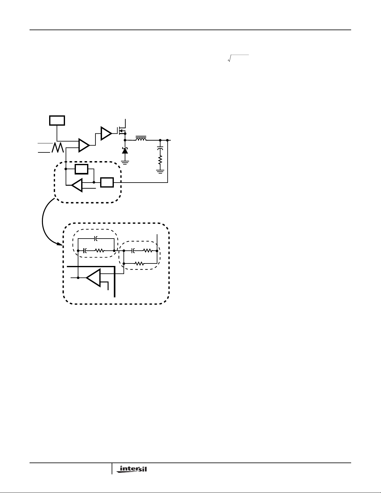
Figure 7 highlights the voltage-mode control loop for a
synchronous-rectified buck converter. The output voltage
(Vout) is regulated to the Reference voltage level. The error
amplifier (Error Amp) output (V
oscillator (OSC) triangular wave to provide a pulse-width
modulated (PWM) wave with an amplitude of Vin at the
PHASE node. The PWM wave is smoothed by the output
filter (Lo and Co).
OSC
PWM
COMPARATOR
-
∆V
OSC
+
Z
FB
V
E/A
-
+
ERROR
AMP
REFERENCE
DETAILED COMPENSATION COMPONENTS
C2
C1
COMP
HIP6013
FIGURE 7. VOLTAGE - MODE BUCK CONVERTER
COMPENSATION DESIGN
The modulator transfer function is the small-signal transfer
function of Vout/V
. This function is dominated by a DC
E/A
Gain and the output filter (Lo and Co), with a double pole
break frequency at F
and a zero at F
LC
the modulator is simply the input voltage (Vin) divided by the
peak-to-peak oscillator voltage ∆V
) is compared with the
E/A
V
DRIVER
DRIVER
Z
R2
-
+
REF
IN
PHASE
IN
Z
FB
FB
ESR
.
OSC
L
O
C
O
ESR
(PARASITIC)
V
OUT
Z
IN
C3
R3
R1
. The DC Gain of
V
OUT
Modulator Break Frequency Equations
F
LC =
2π LOCO••
F
ESR
=
1
-------------------------------------- -
The compensation network consists of the error amplifier
(internal to the HIP6013) and the impedance networks Z
and ZFB. The goal of the compensation network is to provide
a closed loop transfer function with the highest 0dB crossing
frequency (f
) and adequate phase margin. Phase margin
0dB
is the difference between the closed loop phase at f
o
180
. The equations below relate the compensation
network’s poles, zeros and gain to the components (R1, R2,
R3, C1, C2, and C3) in Figure 8. Use these guidelines for
locating the poles and zeros of the compensation network:
1
--------------------------------------------
2π ESR C
•()•
0dB
O
IN
and
Compensation Break Frequency Equations
1
---------------------------------
F
=
Z1
2π R2 C1••
-----------------------------------------------------
FZ2=
2π R1 + R3()• C3•
1
----------------------------------------------------- -
FP1=
2π R2•
---------------------------------
FP2=
2π R3• C3•
1. Pick Gain (R2/R1) for desired converter bandwidth
ST
2. Place 1
(~75% F
3. Place 2
4. Place 1
5. Place 2
Zero Below Filter’s Double Pole
)
LC
ND
Zero at Filter’s Double Pole
ST
Pole at the ESR Zero
ND
Pole at Half the Switching Frequency
6. Check Gain against Error Amplifier’s Open-Loop Gain
7. Estimate Phase Margin - Repeat if Necessary
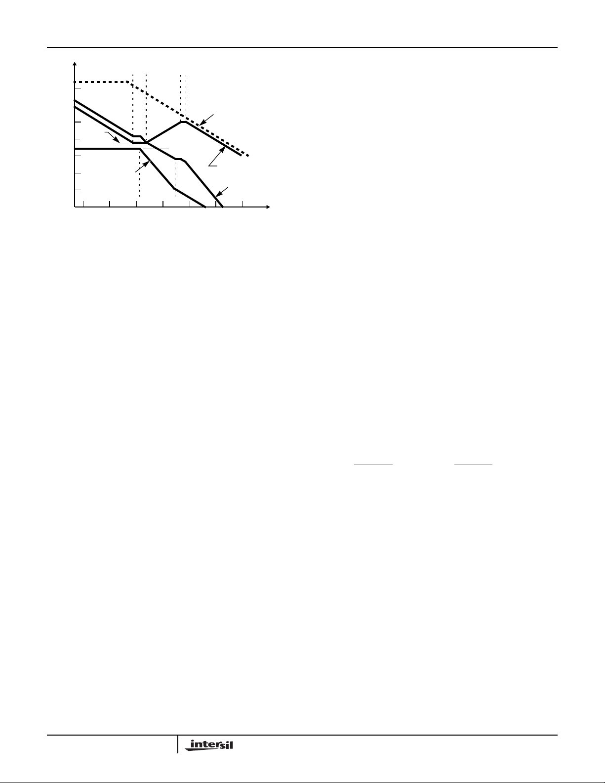
Figure 8 shows an asymptotic plot of the DC-DC converter’s
gain vs frequency. The actual Modulator Gain has a high
gain peak do to the high Q factor of the output filter and is
not shown in Figure 8. Using the above guidelines should
give a Compensation Gain similar to the curve plotted. The
open loop error amplifier gain bounds the compensation
gain. Check the compensation gain at F
capabilities of the error amplifier. The Closed Loop Gain is
constructed on the log-log graph of Figure 8 by adding the
Modulator Gain (in dB) to the Compensation Gain (in dB).
This is equivalent to multiplying the modulator transfer
function to the compensation transfer function and plotting
the gain.
The compensation gain uses external impedance networks
Z
and ZINto provide a stable,high bandwidth (BW) overall
FB
loop. A stable control loop has a gain crossing with
-20dB/decade slope and a phase margin greater than 45
Include worst case component variations when determining
phase margin.
1
C1 C2•
--------------------- -
•
C1 + C2
1
with the
P2
o
.
2-168
Page 8
HIP6013
100
80
60
40
20LOG
(R2/R1)
20
GAIN (dB)
0
MODULATOR
-20
-40
-60
FIGURE 8. ASYMPTOTIC BODE PLOT OF CONVERTER GAIN
GAIN
F
F
F
P1
Z2
Z1
F
LC
F
FREQUENCY (Hz)
(V
ESR
F
P2
20LOG
/∆V
IN
OSC
OPEN LOOP
ERROR AMP GAIN
)
COMPENSATION
GAIN
CLOSED LOOP
GAIN
10M1M100K10K1K10010
Component Selection Guidelines
Output Capacitor Selection
An output capacitor is required to filter the output and supply
the load transient current. The filtering requirements are a
function of the switching frequency and the ripple current.
The load transient requirements are a function of the slew
rate (di/dt) and the magnitude of the transient load current.
These requirements are generally met with a mix of
capacitors and careful layout.
Modern microprocessors produce transient load rates above
1A/ns. High frequency capacitors initially supply the transient
and slow the current load rate seen by the bulk capacitors .
The bulk filter capacitor values are generally determined by
the ESR (effective series resistance) and voltage rating
requirements rather than actual capacitance requirements.
High frequency decoupling capacitors should be placed as
close to the power pins of the load as physically possible. Be
careful not to add inductance in the circuit board wiring that
could cancel the usefulness of these low inductance
components. Consult with the manufacturer of the load on
specific decoupling requirements. For example, Intel
recommends that the high frequency decoupling for the
Pentium-Pro be composed of at least forty (40) 1.0µF
ceramic capacitors in the 1206 surface-mount package.
Use only specialized low-ESR capacitors intended for
switching-regulator applications for the bulk capacitors. The
bulk capacitor’s ESR will determine the output ripple voltage
and the initial voltage drop after a high slew-rate transient.
An aluminum electrolytic capacitor's ESR value is related to
the case size with lower ESR available in larger case sizes.
However, the equivalent series inductance (ESL) of these
capacitors increases with case size and can reduce the
usefulness of the capacitor to high slew-rate transient
loading. Unfortunately, ESL is not a specified parameter.
Work with your capacitor supplier and measure the
capacitor’s impedance with frequency to select a suitable
component. In most cases, multiple electrolytic capacitors of
small case size perform better than a single large case
capacitor.
Output Inductor Selection
The output inductor is selected to meet the output voltage
ripple requirements and minimize the converter’s response
time to the load transient. The inductor value determines the
converter’s ripple current and the ripple voltage is a function
of the ripple current. The ripple voltage and current are
approximated by the following equations:
∆I=
V
IN-VOUT
------------------------------- -
Fs LO×
V
--------------- -
•
OUT
V
IN
∆ V
OUT
= ∆I x ESR
Increasing the value of inductance reduces the ripple current
and voltage. However, the large inductance values reduce
the converter’s response time to a load transient.
One of the parameters limiting the converter’s response to a
load transient is the time required to change the inductor
current. Given a sufficiently fast control loop design, the
HIP6013 will provide either 0% or 100% duty cycle in
response to a load transient. The response time is the time
required to slew the inductor current from an initial current
value to the transient current level. During this interval the
difference between the inductor current and the transient
current level must be supplied b y the output capacitor.
Minimizing the response time can minimize the output
capacitance required.
The response time to a transient is different for the
application of load and the removal of load. The following
equations give the approximate response time interval for
application and removal of a transient load:
x I
L
O
t
=
RISE
where: I
TRAN
VIN - V
O
is the transient load current step, t
TRAN
t
FALL
response time to the application of load, and t
x I
L
O
V
TRAN
O
RISE
FALL
is the
is the
=
response time to the removal of load. With a +5V input
source, the worst case response time can be either at the
application or removal of load and dependent upon the
output voltage setting. Be sure to check both of these
equations at the minimum and maximum output levelsforthe
worst case response time.
Input Capacitor Selection
Use a mix of input bypass capacitors to control the voltage
overshoot across the MOSFETs. Use small ceramic
capacitors for high frequency decoupling and bulk capacitors
to supply the current needed each time Q1 turns on. Place
the small ceramic capacitors physically close to the
MOSFETs and between the drain of Q1 and the anode of
Schottky diode D2.
The important parameters for the bulk input capacitor are the
voltage rating and the RMS current rating. For reliable
2-169
Page 9
HIP6013
operation, select the bulk capacitor with voltage and current
ratings above the maximum input voltage and largest RMS
current required by the circuit. The capacitor voltage rating
should be at least 1.25 times greater than the maximum
input voltage and a voltage rating of 1.5 times is a
conservative guideline. The RMS current rating requirement
for the input capacitor of a buck regulator is approximately
1/2 the DC load current.
For a through hole design, several electrolytic capacitors
(Panasonic HFQ series or Nichicon PL series or Sanyo MVGX or equivalent) may be needed. For surface mount
designs, solid tantalum capacitors can be used, but caution
must be exercised with regard to the capacitor surge current
rating. These capacitors must be capable of handling the
surge-current at power-up. The TPS series available from
AVX, and the 593D series from Sprague are both surge
current tested.
MOSFET Selection/Considerations
The HIP6013 requires an N-Channel power MOSFET. It
should be selected based upon r
requirements, and thermal management requirements.
In high-current applications, the MOSFET power
dissipation, package selection and heatsink are the
dominant design factors. The power dissipation includes
two loss components; conduction loss and switching loss.
The conduction losses are the largest component of power
dissipation for the MOSFET. Switching losses also
contribute to the overall MOSFET power loss (see the
equations below). These equations assume linear voltagecurrent transitions and are approximations. The gatecharge losses are dissipated by the HIP6013 and don't
heat the MOSFET. However, large gate-charge increases
the switching interval, t
, which increases the upper
SW
MOSFET switching losses. Ensure that the MOSFET is
within its maximum junction temperature at high ambient
temperature by calculating the temperature rise according
to package thermal-resistance specifications. A separate
heatsink may be necessary depending upon MOSFET
power, package type, ambient temperature and air flow.
P
COND
P
SW
=
2
= I
x r
O
DS(ON)
1
IO x VIN x tSW x Fs
2
x D
DS(ON)
, gate supply
Standard-gate MOSFETs are normally recommended for
use with the HIP6013. However, logic-level gate MOSFETs
can be used under special circumstances. The input voltage,
upper gate drive level, and the MOSFET’s absolute gate-tosource voltage rating determine whether logic-level
MOSFETs are appropriate.
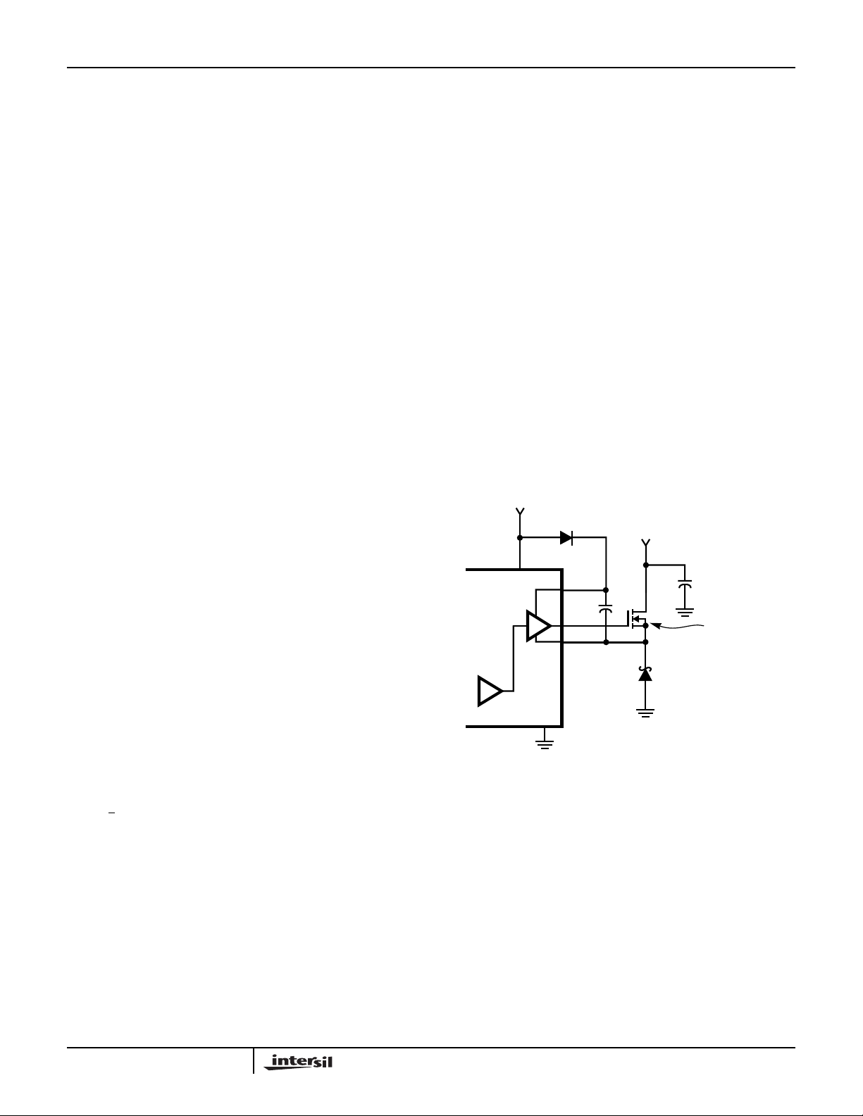
Figure 9 shows the upper gate drive (BOOT pin) supplied by
a bootstrap circuit from V
. The boot capacitor, C
CC
BOOT
develops a floating supply voltage referenced to the PHASE
pin. This supply is refreshed each cycle to a voltage of V
CC
less the boot diode drop (VD) when the lower MOSFET, Q2
turns on. A logic-level MOSFET can only be used for Q1 if
the MOSFET’s absolute gate-to-source voltage rating
exceeds the maximum voltage applied to V
CC
.
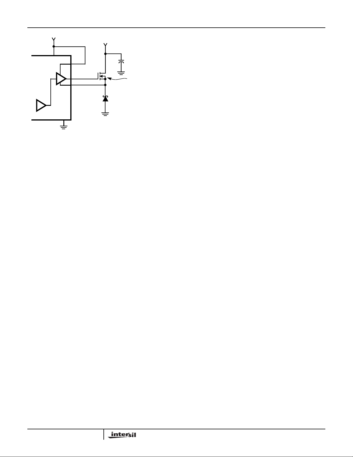
Figure 10 shows the upper gate drive supplied by a direct
connection to VCC. This option should only be used in
converter systems where the main input voltage is +5VDC
or less. The peak upper gate-to-source voltage is
approximately V
less the input supply. For +5V main
CC
power and +12VDC for the bias, the gate-to-source voltage
of Q1 is 7V. A logic-level MOSFET is a good choice for Q1
and a logic-level MOSFET is a good choice for Q1 under
these conditions.
+12V
HIP6013
-
+
FIGURE 9. UPPER GATE DRIVE - BOOTSTRAP OPTION
VCC
D
BOOT
BOOT
UGATE
PHASE
GND
C
BOOT
+5V OR +12V
Q1
D2
NOTE:
V
G-S
≈ V
CC
- V
D
Where: D is the duty cycle = V
is the switching interval, and
t
SW
Fs is the switching frequency.
2-170
/ VIN,
O
Page 10
HIP6013
+12V
VCC
HIP6013
+
FIGURE 10. UPPER GATE DRIVE - DIRECT VCC DRIVE OPTION
BOOT
UGATE
PHASE
GND
+5V OR LESS
Q1
D2
NOTE:
V
G-S
≈ V
CC
- 5V
Schottky Selection
Rectifier D2 conducts when the upper MOSFET Q1 is off.
The diode should be a Schottky type for low power losses.
The power dissipation in the Schottky rectifier is
approximated by:
P
Where: D is the duty cycle = VO/VIN, and
In addition to power dissipation, package selection and
heatsink requirements are the main design tradeoffs in
choosing the Schottky rectifier. Since the three f actors are
interrelated, the selection process is an iterative procedure.
The maximum junction temperature of the rectifier must
remain below the manufacturer’s specified value, typically
125
and the Schottky power dissipation equation (shown abov e),
the junction temperature of the rectifier can be estimated. Be
sure to use the available airflo w and ambient temper ature to
determine the junction temperature rise.
= IO x Vf x (1 - D)
COND
is the schottky forward voltage drop
V
f
o
C.By using the package thermal resistance specification
2-171
Page 11
HIP6013
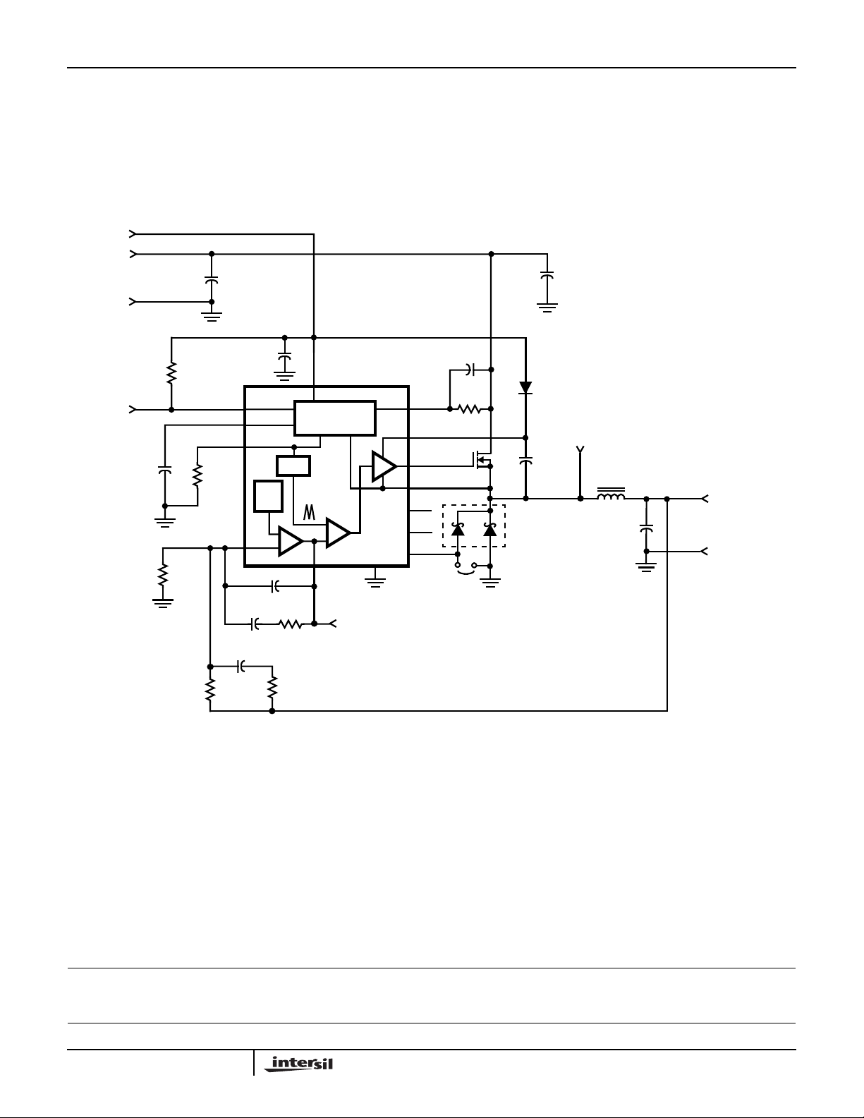
HIP6013 DC-DC Converter Application Circuit
The figure below shows a DC-DC converter circuit for a
microprocessor application, originally designed to employ the
HIP6007 controller. Giv en the similarities between the
HIP6007 and HIP6013 controllers, the circuit can be
implemented using the HIP6013 controller without any
modifications.Howev er, given the expanded reference voltage
12VCC
VIN
C1-5
3x 680µF
RTN
tolerance range, the HIP6013-based conv erter may require
additional output capacitance. Detailed information on the
circuit, including a complete Bill-of-Materials and circuit board
description, can be found in application note AN9722. See
Intersil’s home page on the web:http://www.intersil.com or
Intersil AnswerFAX (407-724-7800) document # 99722.
C17-18
2x 1µF
1206
R7
10K
ENABLE
C13
0.1µF
R2
1K
R3
1K
R1
SPARE
Component Selection Notes:
SS
RT
FB
C15
0.01µF
C16
SPARE
C12
1µF
1206
6
3
1
5
REF
C14
33pF
VCC
14
MONITOR AND
PROTECTION
OSC
U1
HIP6013
+
-
COMP
R5
15K
R4
SPARE
-
+
COMP
TP1
C19
CR3
CR1
4148
C20
0.1µF
PHASE
TP2
L2
C6-11
4x 1000µF
V
OUT
RTN
1000pF
OCSET
2
10
BOOT
9
UGATE
PHASE
8
NC
13
NC
12
NC
11
74
GND
R6
3.01K
Q1
JP1
C1-C3 - 3 each 680µF 25W VDC, Sanyo MV-GX or equivalent.
C6-C9 - 4 each 1000µF 6.3W VDC, Sanyo MV-GX or equivalent.
L1 - Core: Micrometals T60-52; Winding: 14 Turns of 17AWG.
CR1 - 1N4148 or equivalent.
CR3 - 15A, 35V Schottky, Motorola MBR1535CT or equivalent.
Q1 - Intersil MOSFET; RFP25N05.
FIGURE 11. DC-DC CONVERTER APPLICATION CIRCUIT
All Intersil semiconductor products are manufactured, assembled and tested under ISO9000 quality systems certification.
Intersil semiconductor products are sold by description only .Intersil Corporation reserves the right to make changes in circuit design and/or specifications at any time without notice. Accordingly, the reader is cautioned to verify that data sheets are current before placing orders. Information furnished by Intersil is believed to be accurate and
reliable. However, no responsibility is assumed by Intersil or its subsidiaries for its use; nor for any infringements of patents or other rights of third parties which may result
from its use. No license is granted by implication or otherwise under any patent or patent rights of Intersil or its subsidiaries.
For information regarding Intersil Corporation and its products, see web site http://www.intersil.com
2-172
 Loading...