

Page 1
®
www.BDTIC.com/Intersil
HIP2100
Data Sheet October 21, 2004 FN4022.13
100V/2A Peak, Low Cost, High Frequency
Half Bridge Driver
The HIP2100 is a high frequency, 100V Half Bridge
N-Channel power MOSFET driver IC. The low-side and
high-side gate drivers are independently controlled and
matched to 8ns. This gives the user maximum flexibility in
dead-time selection and driver protocol. Undervoltage
protection on both the low-side and high-side supplies force
the outputs low. An on-chip diode eliminates the discrete
diode required with other driver ICs. A new level-shifter
topology yields the low-power benefits of pulsed operation
with the safety of DC operation. Unlike some competitors,
the high-side output returns to its correct state after a
momentary undervoltage of the high-side supply.
Ordering Information
PART #
HIP2100IB -40 to 125 8 Ld SOIC M8.15
HIP2100IBZ (Note 1) -40 to 125 8 Ld SOIC (Pb-free) M8.15
HIP2100EIB -40 to 125 8 Ld EPSOIC M8.15C
HIP2100EIBZ
(Note 1)
HIP2100IR -40 to 125 16 Ld 5x5 QFN L16.5x5
HIP2100IRZ (Note 1) -40 to 125 16 Ld 5x5 QFN
HIP2100IR4 -40 to 125 12 Ld 4x4 DFN L12.4x4A
HIP2100IR4Z
(Note 1)
NOTES:
1. Intersil Pb-free products employ special Pb-free material sets;
molding compounds/die attach materials and 100% matte tin
plate termination finish, which are RoHS compliant and
compatible with both SnPb and Pb-free soldering operations.
Intersil Pb-free products are MSL classified at Pb-free peak
reflow temperatures that meet or exceed the Pb-free
requirements of IPC/JEDEC J STD-020C.
2. Add “T” suffix for Tape and Reel packing option.
TEMP.
RANGE (°C) PACKAGE
-40 to 125 8 Ld EPSOIC
(Pb-free)
(Pb-free)
-40 to 125 12 Ld 4x4 DFN
(Pb-free)
PKG.
DWG. #
M8.15C
L16.5x5
L12.4x4A
Features
• Drives N-Channel MOSFET Half Bridge
• SOIC, EPSOIC, QFN and DFN Package Options
• SOIC, EPSOIC and DFN Packages Compliant with 100V
Conductor Spacing Guidelines of IPC-2221
• Pb-Free Product Available (RoHS Compliant)
• Bootstrap Supply Max Voltage to 114VDC
• On-Chip 1Ω Bootstrap Diode
• Fast Propagation Times for Multi-MHz Circuits
• Drives 1000pF Load with Rise and Fall Times Typ. 10ns
• CMOS Input Thresholds for Improved Noise Immunity
• Independent Inputs for Non-Half Bridge Topologies
• No Start-Up Problems
• Outputs Unaffected by Supply Glitches, HS Ringing Below
Ground, or HS Slewing at High dv/dt
• Low Power Consumption
• Wide Supply Range
• Supply Undervoltage Protection
•3Ω Driver Output Resistance
• QFN/DFN Package:
- Compliant to JEDEC PUB95 MO-220
QFN - Quad Flat No Leads - Package Outline
- Near Chip Scale Package footprint, which improves
PCB efficiency and has a thinner profile
Applications
• Telecom Half Bridge Power Supplies
• Avionics DC-DC Converters
• Two-Switch Forward Converters
• Active Clamp Forward Converters
1
CAUTION: These devices are sensitive to electrostatic discharge; follow proper IC Handling Procedures.
1-888-INTERSIL or 321-724-7143
| Intersil (and design) is a registered trademark of Intersil Americas Inc.
All other trademarks mentioned are the property of their respective owners.
Copyright © Intersil Americas Inc. 2004. All Rights Reserved.
Page 2
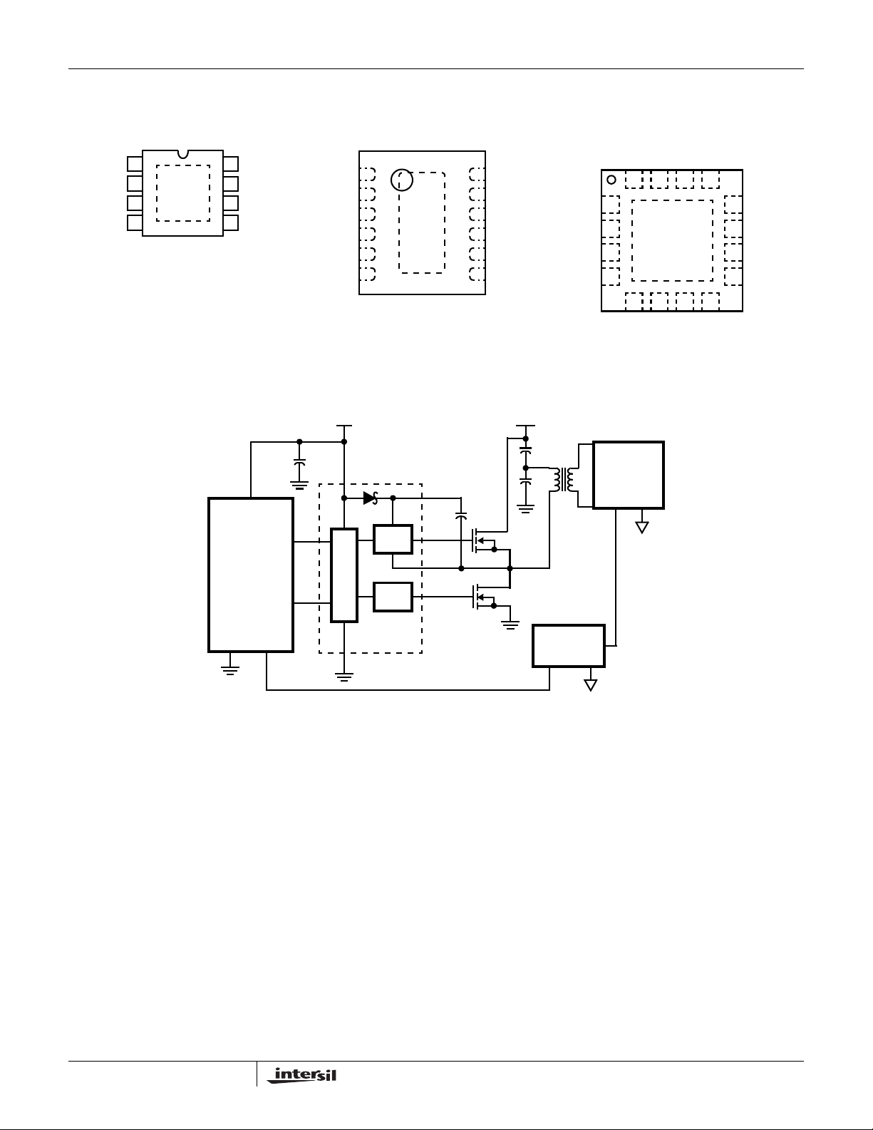
Pinouts
www.BDTIC.com/Intersil
HIP2100 (SOIC, EPSOIC)
TOP VIEW
1
V
DD
HB
2
HO
HS
EPAD
3
4
8
LO
V
7
SS
LI
6
HI
5
NOTE: EPAD = Exposed PAD.
Application Block Diagram
HIP2100
HIP2100IR4 (DFN)
TOP VIEW
V
1
DD
NC
2
NC
3
HB
4
HO
5
6 7HI
HS
EPAD
HIP2100 (QFN)
TOP VIEW
VDDLO
LO
12
11
V
SS
10
NC
9
NC
8
LI
NC
HB
HO
NC
NC
15
16 14 13
1
2
3
4
EPAD
6578
HS
NC
NC
12
NC
11
V
SS
10
LI
NC
9
HI
NC
PWM
CONTROLLER
+12V
V
DD
HB
HI
LI
DRIVE
DRIVE
CONTROL
HIP2100
V
SS
HI
LO
HO
HS
LO
+100V
REFERENCE
AND
ISOLATION
SECONDARY
CIRCUIT
2
FN4022.13
Page 3
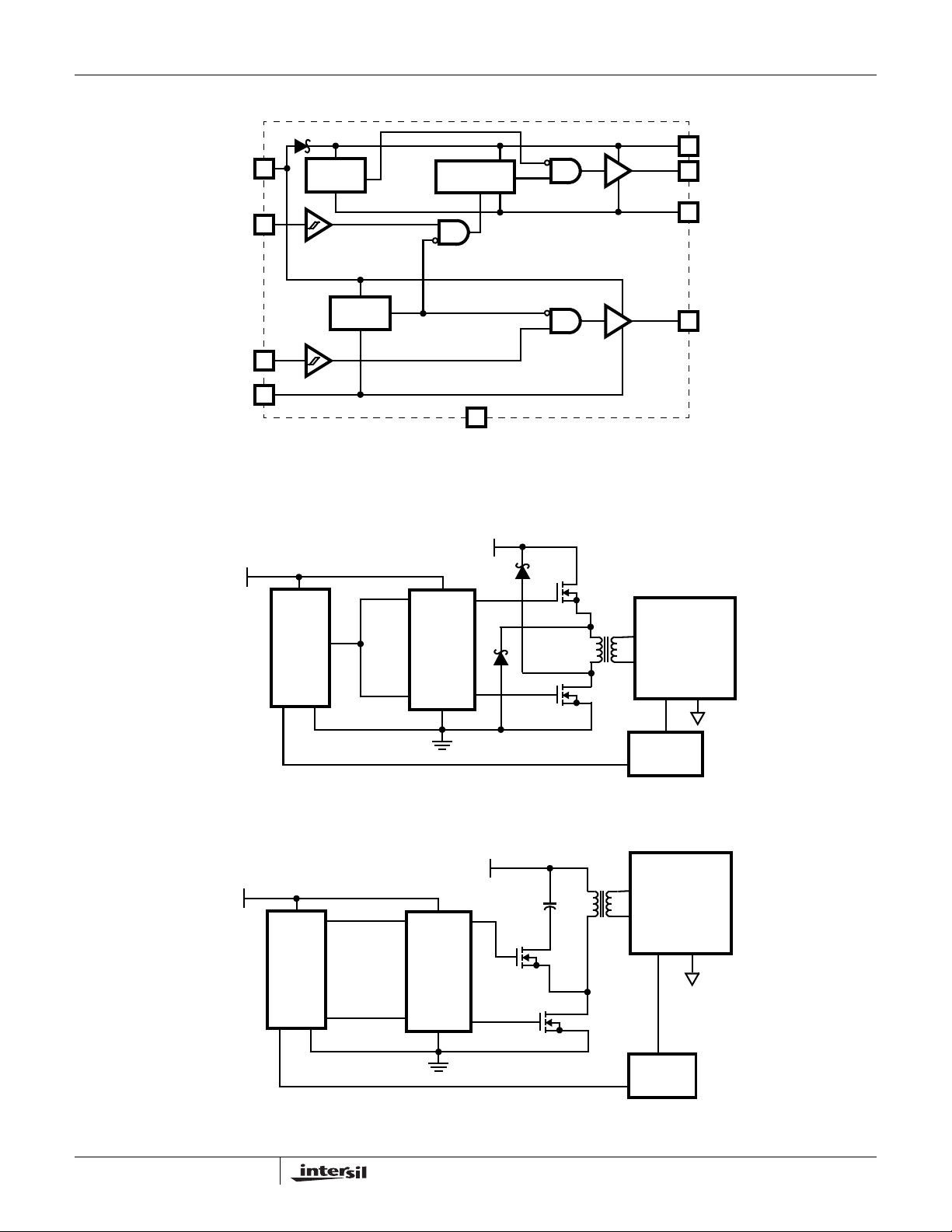
Functional Block Diagram
www.BDTIC.com/Intersil
V
DD
HI
LI
V
SS
*EPAD = Exposed Pad. The EPAD is electrically isolated from all other pins. For
best thermal performance connect the EPAD to the PCB power ground plane.
UNDER
VOLTAGE
UNDER
VOLTAGE
HIP2100
LEVEL SHIFT
EPAD (EPSOIC, QFN and DFN PACKAGES ONLY)
HB
HO
DRIVER
HS
LO
DRIVER
+12V
+12V
+48V
PWM
FIGURE 1. TWO-SWITCH FORWARD CONVERTER
PWM
HIP2100
+48V
HIP2100
SECONDARY
CIRCUIT
ISOLATION
SECONDARY
CIRCUIT
FIGURE 2. FORWARD CONVERTER WITH AN ACTIVE CLAMP
3
ISOLATION
FN4022.13
Page 4
HIP2100
www.BDTIC.com/Intersil
Absolute Maximum Ratings Thermal Information
Supply Voltage, V
LI and HI Voltages (Note 4) . . . . . . . . . . . . . . . . -0.3V to V
Voltage on LO (Note 4) . . . . . . . . . . . . . . . . . . . -0.3V to V
Voltage on HO (Note 4) . . . . . . . . . . . . . . . V
Voltage on HS (Continuous) (Note 4) . . . . . . . . . . . . . . -1V to 110V
Voltage on HB (Note 4) . . . . . . . . . . . . . . . . . . . . . . . . . . . . . +118V
Average Current in V
ESD Classification . . . . . . . . . . . . . . . . . . . . . . . . . . . Class 1 (1kV)
DD, VHB-VHS
DD
Maximum Recommended Operating Conditions
Supply Voltage, VDD . . . . . . . . . . . . . . . . . . . . . . . . +9V to 14.0VDC
Voltage on HS . . . . . . . . . . . . . . . . . . . . . . . . . . . . . . . . -1V to 100V
Voltage on HS. . . . . . . . . . . . . . . .(Repetitive Transient) -5V to 105V
Voltage on HB . . . V
HS Slew Rate. . . . . . . . . . . . . . . . . . . . . . . . . . . . . . . . . . . . <50V/ns
CAUTION: Stresses above those listed in “Absolute Maximum Ratings” may cause permanent damage to the device. This is a stress only rating and operation of the
device at these or any other conditions above those indicated in the recommended operating conditions of this specification is not implied.
NOTES:
3. The HIP2100 is capable of derated operation at supply voltages exceeding 14V. Figure 16 shows the high-side voltage derating curve for this
mode of operation.
4. All voltages referenced to V
is measured with the component mounted on a high effective thermal conductivity test board in free air. See Tech Brief TB379 for details.
5. θ
JA
is measured in free air with the component mounted on a high effective thermal conductivity test board with “direct attach” features. θ
6. θ
JA
“case temp” is measured at the center of the exposed metal pad on the package underside. See Tech Brief TB379.
+8V to VHS+14.0V and VDD-1V to VDD+100V
HS
(Notes 3, 4) . . . . . . . . -0.3V to 18V
-0.3V to VHB +0.3V
HS
to HB diode . . . . . . . . . . . . . . . . . . . 100mA
unless otherwise specified.
SS
DD
DD
+0.3V
+0.3V
Thermal Resistance (Typical) θ
SOIC (Note 5) . . . . . . . . . . . . . . . . . . . 95 N/A
EPSOIC (Note 6) . . . . . . . . . . . . . . . . . 40 3.0
QFN (Note 6) . . . . . . . . . . . . . . . . . . . . 37 6.5
DFN (Note 6) . . . . . . . . . . . . . . . . . . . . 40 3.0
Max Power Dissipation at 25°C in Free Air (SOIC, Note 5). . . . . . 1.3W
Max Power Dissipation at 25°C in Free Air (EPSOIC, Note 6) . . . 3.1W
Max Power Dissipation at 25°C in Free Air (QFN, Note 6) . . . . . . 3.3W
Storage Temperature Range . . . . . . . . . . . . . . . . . . . -65°C to 150°C
Junction Temperature Range. . . . . . . . . . . . . . . . . . . -55°C to 150°C
Lead Temperature (Soldering 10s - SOIC Lead Tips Only) . . 300°C
For Recommended soldering conditions see Tech Brief TB389.
(°C/W) θJC (°C/W)
JA
JC,
the
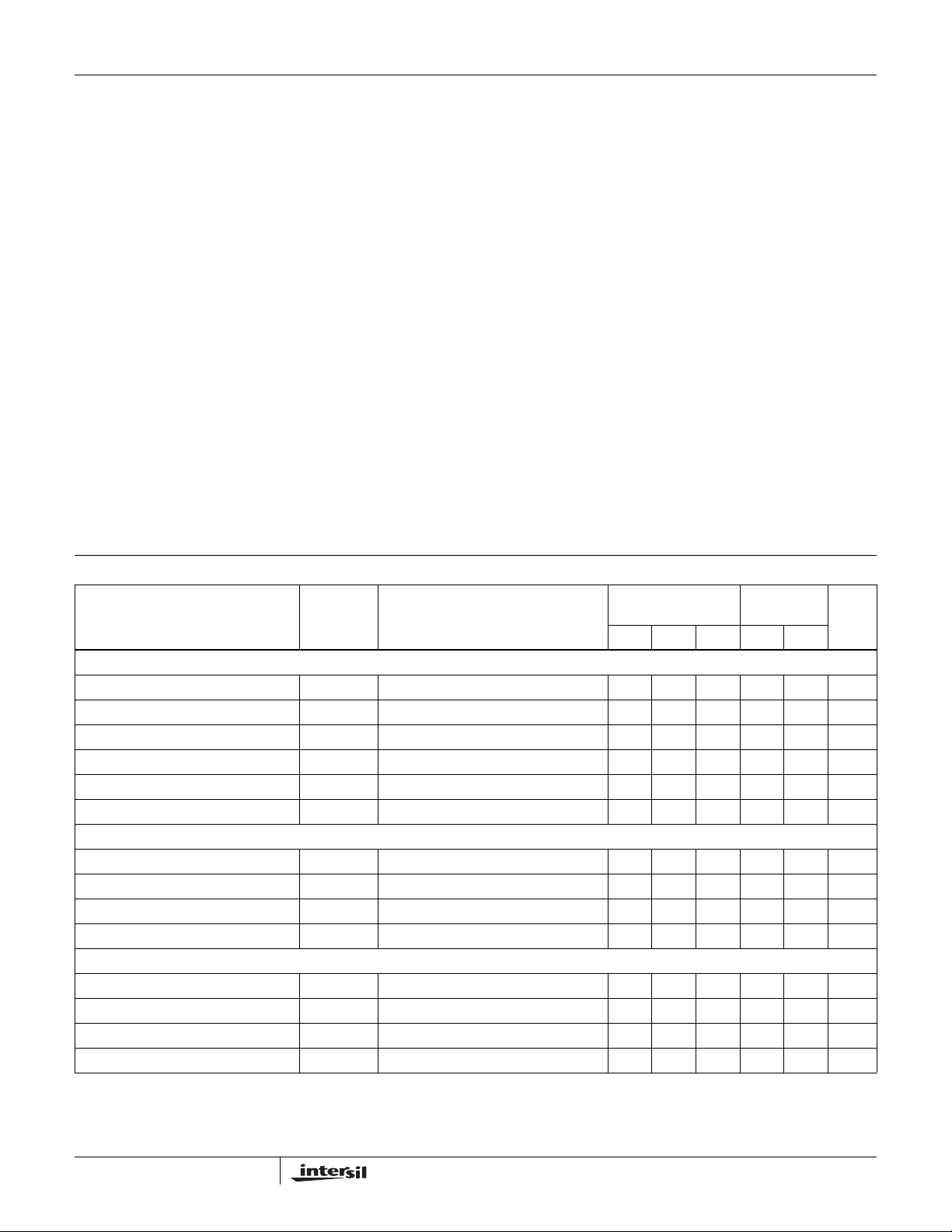
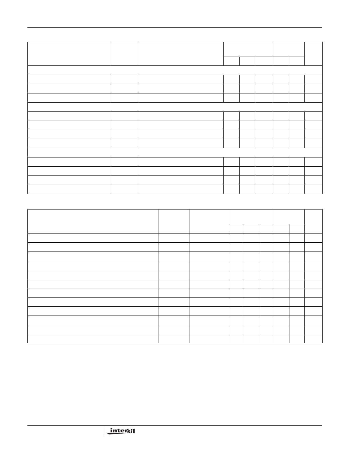
Electrical Specifications V
PARAMETERS SYMBOL TEST CONDITIONS
SUPPLY CURRENTS
Quiescent Current I
V
DD
VDD Operating Current I
Total HB Quiescent Current I
Total HB Operating Current I
HB to V
HB to V
INPUT PINS
Low Level Input Voltage Threshold V
High Level Input Voltage Threshold V
Input Voltage Hysteresis V
Input Pulldown Resistance R
UNDERVOLTAGE PROTECTION
V
V
HB Rising Threshold V
HB Threshold Hysteresis V
Current, Quiescent I
SS
Current, Operating I
SS
Rising Threshold V
DD
Threshold Hysteresis V
DD
DD
= V
HB
= 12V, V
DD
DDO
HB
HBO
HBS
HBSO
IL
IH
IHYS
I
DDR
DDH
HBR
HBH
= V
SS
LI = HI = 0V - 0.1 0.15 - 0.2 mA
f = 500kHz - 1.5 2.5 - 3 mA
LI = HI = 0V - 0.1 0.15 - 0.2 mA
f = 500kHz - 1.5 2.5 - 3 mA
VHS = VHB = 114V - 0.05 1 - 10 µA
f = 500kHz - 0.7 - - - mA
= 0V, No Load on LO or HO, Unless Otherwise Specified
HS
= 25°C
T
J
45.4 - 3 - V
-5.87 - 8 V
-0.4---V
- 200 - 100 500 kΩ
7 7.3 7.8 6.5 8 V
-0.5---V
6.5 6.9 7.5 6 8 V
-0.4---V
T
= -40°C TO
J
125°C
UNITSMIN TYP MAX MIN MAX
4
FN4022.13
Page 5
HIP2100
www.BDTIC.com/Intersil
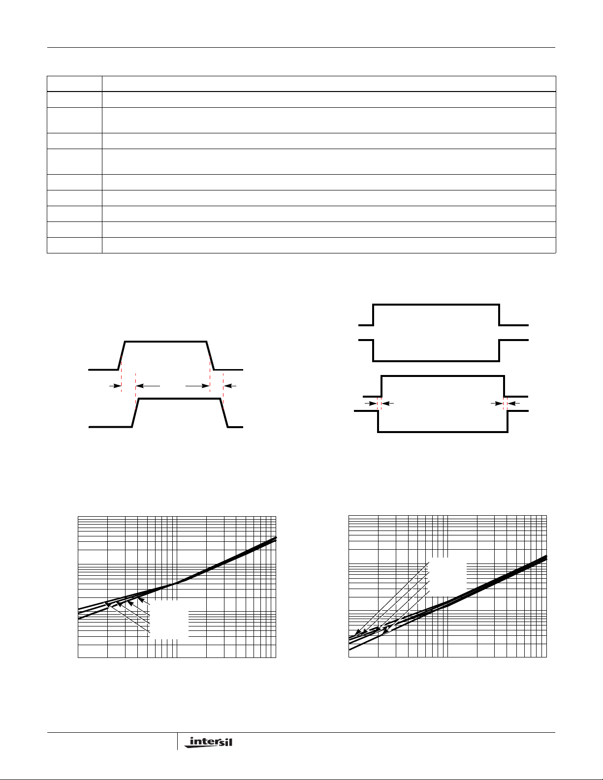
Electrical Specifications V
PARAMETERS SYMBOL TEST CONDITIONS
BOOT STRAP DIODE
Low-Current Forward Voltage V
High-Current Forward Voltage V
Dynamic Resistance R
LO GATE DRIVER
Low Level Output Voltage V
High Level Output Voltage V
Peak Pullup Current I
Peak Pulldown Current I
HO GATE DRIVER
Low Level Output Voltage V
High Level Output Voltage V
Peak Pullup Current I
Peak Pulldown Current I
DD
= V
HB
= 12V, V
DL
DH
D
OLL
OHL
OHL
OLL
OLH
OHH
OHH
OLH
= V
SS
I
VDD-HB
I
VDD-HB
I
VDD-HB
ILO = 100mA - 0.25 0.3 - 0.4 V
ILO = -100mA, V
VLO = 0V -2---A
VLO = 12V - 2 - - - A
IHO = 100mA - 0.25 0.3 - 0.4 V
IHO = -100mA, V
VHO = 0V -2---A
VHO = 12V - 2 - - - A
= 0V, No Load on LO or HO, Unless Otherwise Specified (Continued)
HS
= -40°C TO
T
T
= 25°C
J
= 100µA - 0.45 0.55 - 0.7 V
= 100mA - 0.7 0.8 - 1 V
= 100mA - 0.8 1 - 1.5 Ω
OHL
OHH
= VDD-V
= VHB-V
LO
HO
- 0.25 0.3 - 0.4 V
- 0.25 0.3 - 0.4 V
J
125°C
UNITSMIN TYP MAX MIN MAX
Switching Specifications V
PARAMETERS SYMBOL
Lower Turn-Off Propagation Delay (LI Falling to LO Falling) t
Upper Turn-Off Propagation Delay (HI Falling to HO Falling) t
Lower Turn-On Propagation Delay (LI Rising to LO Rising) t
Upper Turn-On Propagation Delay (HI Rising to HO Rising) t
Delay Matching: Lower Turn-On and Upper Turn-Off t
Delay Matching: Lower Turn-Off and Upper Turn-On t
Either Output Rise/Fall Time t
Either Output Rise/Fall Time (3V to 9V) t
Either Output Rise Time Driving DMOS t
Either Output Fall Time Driving DMOS t
Minimum Input Pulse Width that Changes the Output t
Bootstrap Diode Turn-On or Turn-Off Time t
= VHB = 12V, VSS = VHS = 0V, No Load on LO or HO, Unless Otherwise Specified
DD
LPHL
HPHL
LPLH
HPLH
MON
MOFF
RC, tFC
, t
R
F
RD
FD
PW
BS
T
= -40°C
T
= 25°C
TEST
CONDITIONS
CL = 1000pF - 10 - - - ns
CL = 0.1µF - 0.5 0.6 - 0.8 us
CL = IRFR120 - 20 - - - ns
CL = IRFR120 - 10 - - - ns
J
- 20 35 - 45 ns
- 20 35 - 45 ns
- 20 35 - 45 ns
- 20 35 - 45 ns
- 2 8 - 10 ns
- 2 8 - 10 ns
----50ns
-10- - - ns
J
TO 125°C
UNITSMIN TYP MAX MIN MAX
5
FN4022.13
Page 6
HIP2100
www.BDTIC.com/Intersil
Pin Descriptions
SYMBOL DESCRIPTION
V
DD
Positive Supply to lower gate drivers. De-couple this pin to VSS. Bootstrap diode connected to HB.
HB High-Side Bootstrap supply. External bootstrap capacitor is required. Connect positive side of bootstrap capacitor to this pin.
Bootstrap diode is on-chip.
HO High-Side Output. Connect to gate of High-Side power MOSFET.
HS High-Side Source connection. Connect to source of High-Side power MOSFET. Connect negative side of bootstrap capacitor to
this pin.
HI High-Side input.
LI Low-Side input.
V
SS
Chip negative supply, generally will be ground.
LO Low-Side Output. Connect to gate of Low-Side power MOSFET.
EPAD Exposed Pad. Connect to ground or float. The EPAD is electrically isolated from all other pins.
Timing Diagrams
LI
HI,
LI
t
,
HPLH
t
LPLH
HO,
LO
FIGURE 3.
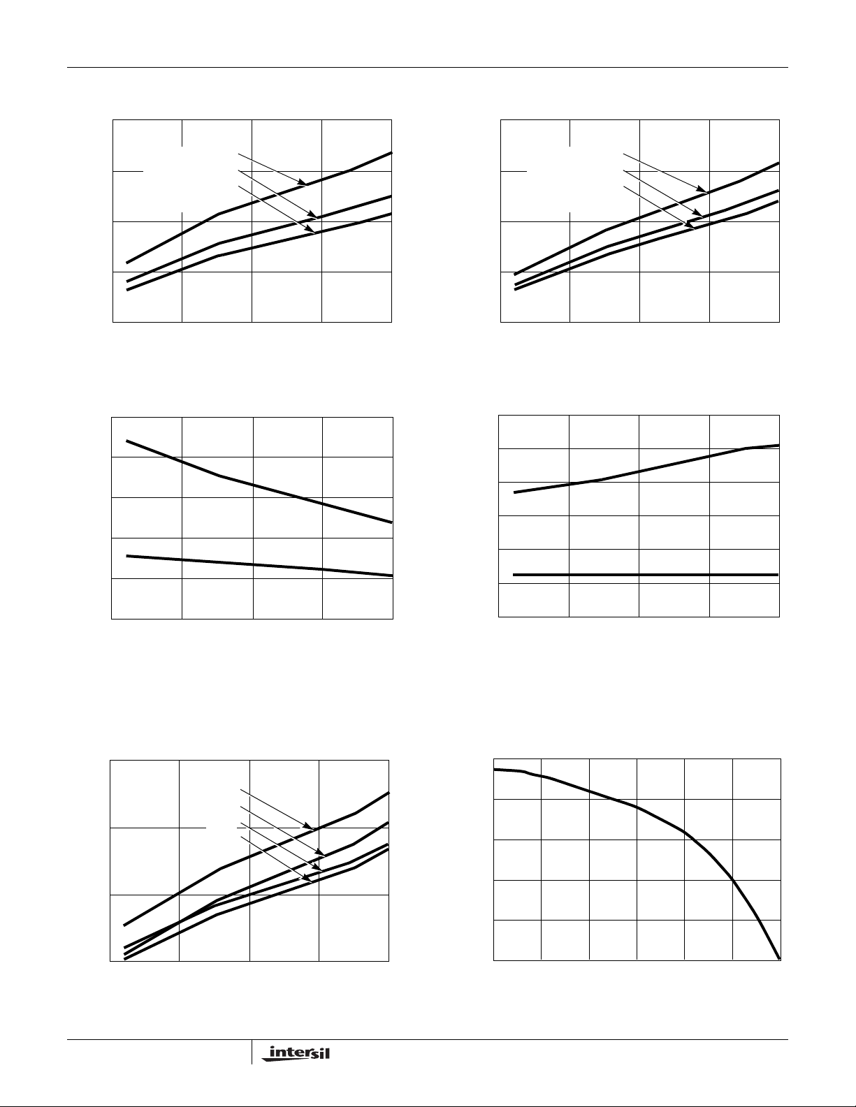
Typical Performance Curves
10
1
(mA)
HBO
, I
DDO
I
0.1
T = 150°C
T = 125°C
T = 25°C
T = -40°C
t
HPHL
t
LPHL
HI
,
LO
HO
t
MON
t
MOFF
FIGURE 4.
10
T = 150°C
T = -40°C
T = 125°C
T = 25°C
(mA)
HBSO
I
1
0.1
0.01
10 100 1000
FREQUENCY (kHz)
FIGURE 5. OPERATING CURRENT vs FREQUENCY
0.01
10 100 1000
FIGURE 6. HB TO V
6
OPERATING CURRENT vs
SS
FREQUENCY
FREQUENCY (kHz)
FN4022.13
Page 7
Typical Performance Curves (Continued)
www.BDTIC.com/Intersil
HIP2100
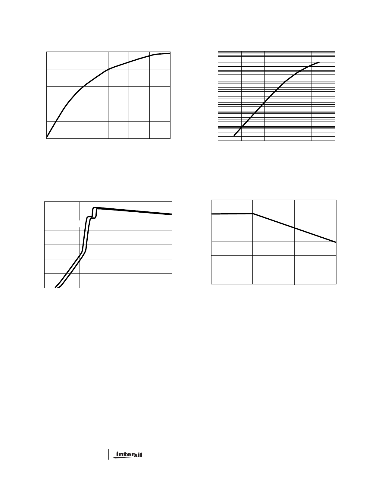
500
VHB = VDD = 9V
V
400
(mV)
300
OHH
, V
OHL
V
200
100
-50 0 50 100
= VDD = 12V
HB
V
= VDD = 14V
HB
150
TEMPERATURE (°C)
FIGURE 7. HIGH LEVEL OUTPUT VOLTAGE vs TEMPERATURE
7.6
7.4
V
V
DDR
HBR
(V)
DDR
, V
HBR
V
7.2
7.0
6.8
500
VHB = VDD = 9V
V
400
(mV)
300
OLH
, V
OLL
V
200
100
-50 0 50 100 150
= VDD = 12V
HB
V
= VDD = 14V
HB
TEMPERATURE (°C)
FIGURE 8. LOW LEVEL OUTPUT VOLTAGE vs TEMPERATURE
0.54
0.5
V
V
DDH
HBH
(mV)
DDH
, V
HBH
V
0.46
0.42
0.38
0.34
6.6
-50 0 50 100 150
TEMPERATURE (°C)
FIGURE 9. UNDERVOLTAGE LOCKOUT THRESHOLD vs
TEMPERATURE
30
t
HPHL
t
(ns)
25
HPHL
, t
HPLH
, t
20
LPHL
, t
LPLH
t
15
-50 0 50 100 150
HPLH
t
LPHL
t
LPLH
TEMPERATURE (°C)
FIGURE 11. PROPAGATION DELAYS vs TEMPERATURE
0.3
-50 0 50 100 150
TEMPERATURE (°C)
FIGURE 10. UNDERVOLTAGE LOCKOUT HYSTERESIS vs
TEMPERATURE
2.5
2.0
1.5
(A)
LO
, I
1.0
HO
I
0.5
0
V
HO
6
, VLO (V)
FIGURE 12. PEAK PULLUP CURRENT vs OUTPUT VOLTAGE
12108420
7
FN4022.13
Page 8
Typical Performance Curves (Continued)
www.BDTIC.com/Intersil
HIP2100
2.5
2.0
1.5
(A)
HO
, I
1.0
LO
I
0.5
0
V
LO
6
, VHO (V)
FIGURE 13. PEAK PULLDOWN CURRENT vs OUTPUT
VO LTAGE
60
50
I
vs V
HB
HB
40
IDD vs V
(µA)
30
HB
, I
DD
I
20
10
DD
1
0.1
0.01
0.001
-4
1•10
FORWARD CURRENT (A)
-5
1•10
12108420
1•10-6
FORWARD VOLTAGE (V)
0.70.60.50.40.3
0.8
FIGURE 14. BOOTSTRAP DIODE I-V CHARACTERISTICS
120
100
80
60
VOLTAGE (V)
SS
40
TO V
HS
20
V
0
0 5 10 15
VDD, VHB (V)
FIGURE 15. QUIESCENT CURRENT vs VOLTAGE
8
0
FIGURE 16. V
14 15 1612
VDD TO VSS VOLTAGE (V)
VOLTAGE vs VDD VOLTAGE
HS
FN4022.13
Page 9
HIP2100
www.BDTIC.com/Intersil
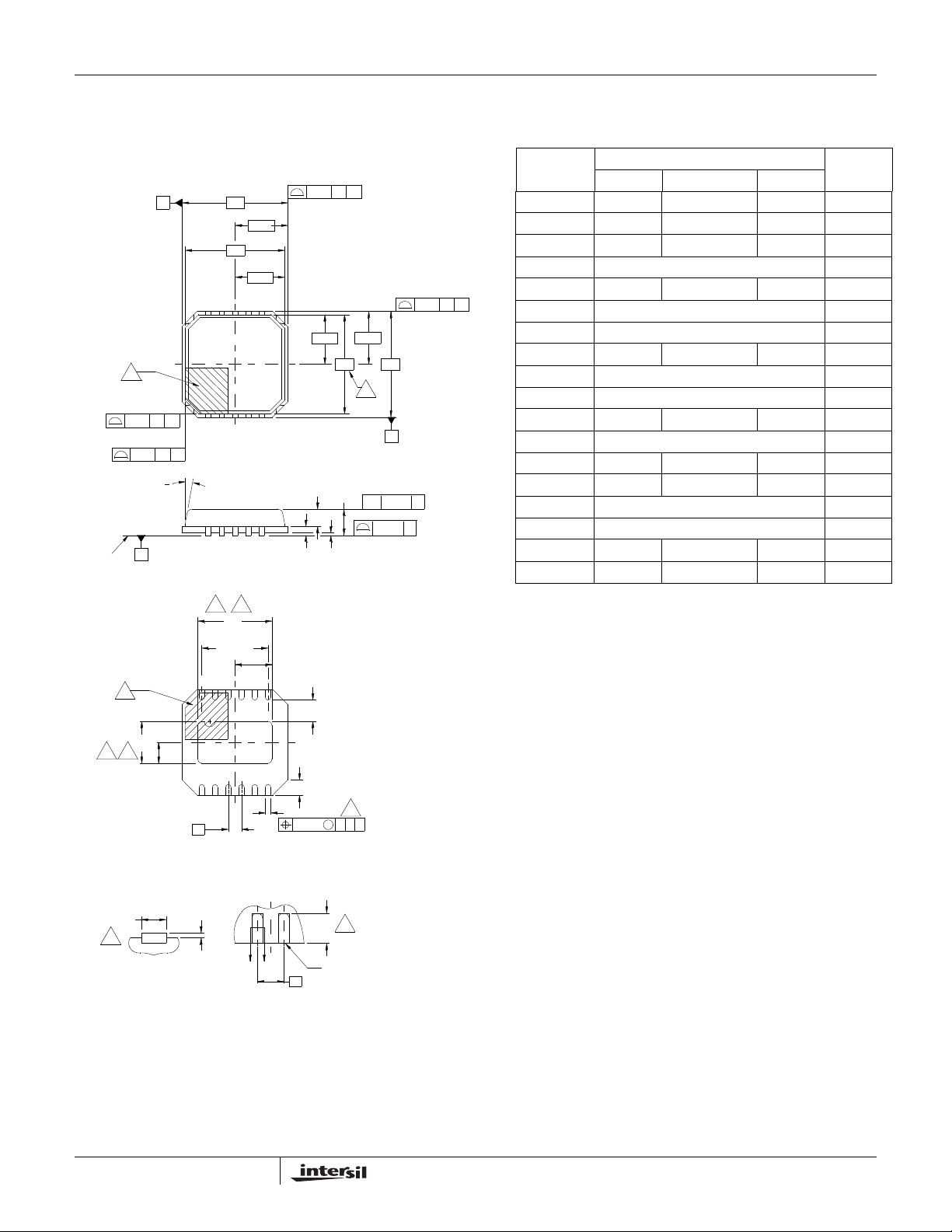
Dual Flat No-Lead Plastic Package (DFN)
Micro Lead Frame Plastic Package (MLFP)
2X
0.15
A
C
E1/2 E/2
A2
A1
A3
NX k
4X P
M
0.10 C A
L
E1 E
9
A
//
0.08 C
5
B
5
B
0.10
2X
0.15
C
SEATING
PLANE
NX b
7
5
INDEX
AREA
2X
2X
INDEX
AREA
6
6
0.15
8
N
1
2
TOP VIEW
SIDE VIEW
7 8
(Nd-1)Xe
1
N
N-1
e
D
D/2
D1
D1/2
3
D2
REF.
D2/2
32
NX b
A
C
B
AC0.15
0
4X
C
E2
E2/2
BOTTOM VIEW
C
L
A1
L12.4x4A
12 LEAD DUAL FLAT NO-LEAD PLASTIC PACKAGE
MILLIMETERS
SYMBOL
A - 0.85 0.90 A1 0.00 0.01 0.05 A2 - 0.65 0.70 A3 0.20 REF -
b 0.18 0.23 0.30 5, 8
B
C
D 4.00 BSC D1 3.75 BSC D2 2.65 2.80 2.95 7, 8
E 4.00 BSC E1 3.75 BSC E2 1.43 1.58 1.73 7, 8
e 0.50 BSC k 0.635 - - L 0.30 0.40 0.50 8
N122
Nd 6 3
P 0.24 0.42 0.60 -
θ --12-
NOTES:
1. Dimensioning and tolerancing conform to ASME Y14.5M-1994.
2. N is the number of terminals.
3. Nd refer to the number of terminals on D.
4. All dimensions are in millimeters. Angles are in degrees.
5. Dimension b applies to the metallized terminal and is measured
between 0.15mm and 0.30mm from the terminal tip.
6. The configuration of the pin #1 identifier is optional, but must be
located within the zone indicated. The pin #1 identifier may be
either a mold or mark feature.
7. Dimensions D2 and E2 are for the exposed pads which provide
improved electrical and thermal performance.
8. Nominal dimensions are provided to assist with PCB Land Pattern
Design efforts, see Intersil Technical Brief TB389.
9. COMPLIANT TO JEDEC MO-229-VGGD-2 ISSUE C except for
the L dimension.
NOTESMIN NOMINAL MAX
Rev. 0 8/03
CC
TERMINAL TIP
e
FOR EVEN TERMINAL/SIDE
9
FN4022.13
Page 10
HIP2100
www.BDTIC.com/Intersil
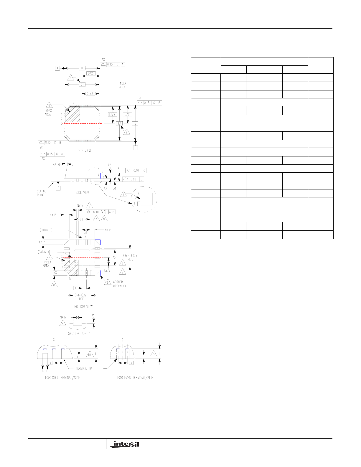
Quad Flat No-Lead Plastic Package (QFN)
Micro Lead Frame Plastic Package (MLFP)
L16.5x5
16 LEAD QUAD FLAT NO-LEAD PLASTIC PACKAGE
(COMPLIANT TO JEDEC MO-220VHHB ISSUE C)
MILLIMETERS
SYMBOL
A 0.80 0.90 1.00 -
A1 - - 0.05 -
A2 - - 1.00 9
A3 0.20 REF 9
b 0.28 0.33 0.40 5, 8
D 5.00 BSC -
D1 4.75 BSC 9
D2 2.55 2.70 2.85 7, 8
E 5.00 BSC -
E1 4.75 BSC 9
E2 2.55 2.70 2.85 7, 8
e 0.80 BSC -
k0.25 - - -
L 0.35 0.60 0.75 8
L1 - - 0.15 10
N162
Nd 4 3
Ne 4 4 3
P- -0.609
θ --129
NOTES:
1. Dimensioning and tolerancing conform to ASME Y14.5-1994.
2. N is the number of terminals.
3. Nd and Ne refer to the number of terminals on each D and E.
4. All dimensions are in millimeters. Angles are in degrees.
5. Dimension b applies to the metallized terminal and is measured
between 0.15mm and 0.30mm from the terminal tip.
6. The configuration of the pin #1 identifier is optional, but must be
located within the zone indicated. The pin #1 identifier may be
either a mold or mark feature.
7. Dimensions D2 and E2 are for the exposed pads which provide
improved electrical and thermal performance.
8. Nominal dimensions are provided to assist with PCB Land Pattern
Design efforts, see Intersil Technical Brief TB389.
9. Features and dimensions A2, A3, D1, E1, P & θ are present when
Anvil singulation method is used and not present for saw
singulation.
10. Depending on the method of lead termination at the edge of the
package, a maximum 0.15mm pull back (L1) maybe present. L
minus L1 to be equal to or greater than 0.3mm.
NOTESMIN NOMINAL MAX
Rev. 2 10/02
10
FN4022.13
Page 11
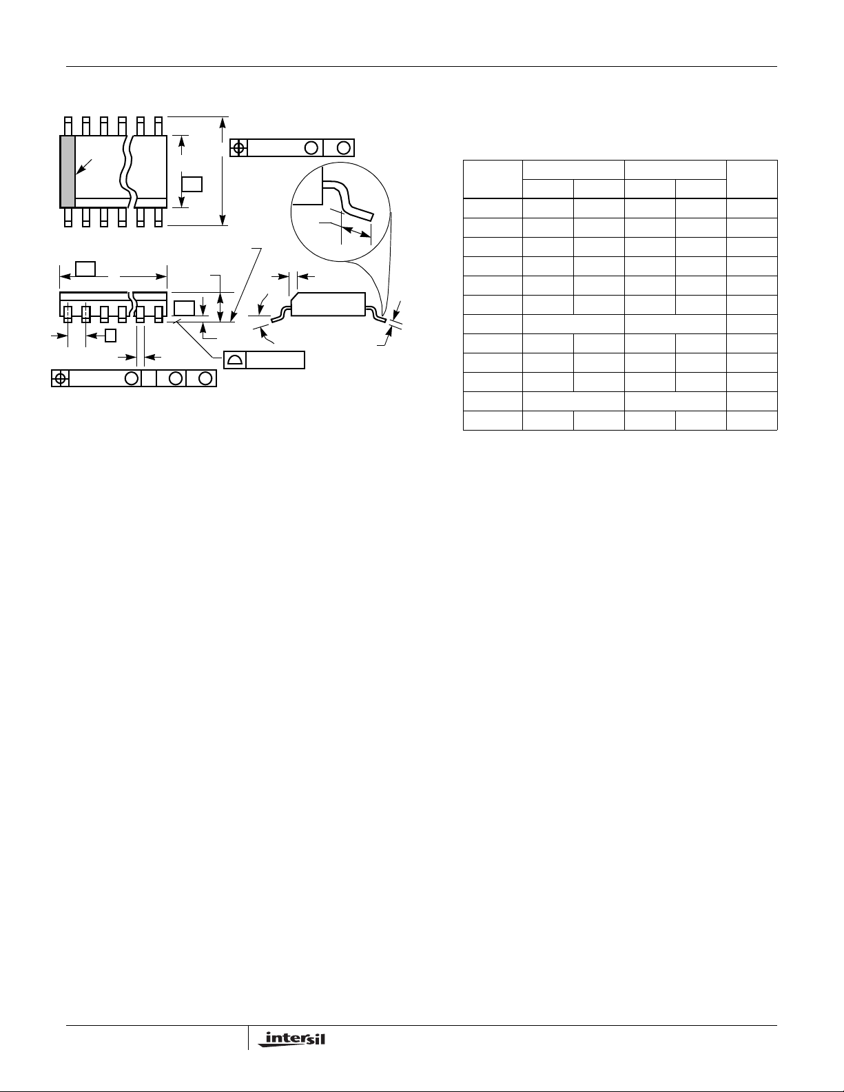
Small Outline Plastic Packages (SOIC)
www.BDTIC.com/Intersil
HIP2100
N
INDEX
AREA
123
-AD
e
B
0.25(0.010) C AM BS
NOTES:
1. Symbols are defined in the “MO Series Symbol List” in Section 2.2 of
Publication Number 95.
2. Dimensioning and tolerancing per ANSI Y14.5M-1982.
3. Dimension “D” does not include mold flash, protrusions or gate burrs.
Mold flash, protrusion and gate burrs shall not exceed 0.15mm (0.006
inch) per side.
4. Dimension “E” does not include interlead flash or protrusions. Interlead flash and protrusions shall not exceed 0.25mm (0.010 inch) per
side.
5. The chamfer on the body is optional. If it is not present, a visual index
feature must be located within the crosshatched area.
6. “L” is the length of terminal for soldering to a substrate.
7. “N” is the number of terminal positions.
8. Terminal numbers are shown for reference only.
9. The lead width “B”, as measured 0.36mm (0.014 inch) or greater
above the seating plane, shall not exceed a maximum value of
0.61mm (0.024 inch).
10. Controlling dimension: MILLIMETER. Converted inch dimensions
are not necessarily exact.
E
-B-
SEATING PLANE
A
-C-
M
0.25(0.010) BM M
H
α
µ
A1
0.10(0.004)
L
h x 45
o
C
M8.15 (JEDEC MS-012-AA ISSUE C)
8 LEAD NARROW BODY SMALL OUTLINE PLASTIC
PACKAGE
INCHES MILLIMETERS
SYMBOL
A 0.0532 0.0688 1.35 1.75 -
A1 0.0040 0.0098 0.10 0.25 -
B 0.013 0.020 0.33 0.51 9
C 0.0075 0.0098 0.19 0.25 -
D 0.1890 0.1968 4.80 5.00 3
E 0.1497 0.1574 3.80 4.00 4
e 0.050 BSC 1.27 BSC -
H 0.2284 0.2440 5.80 6.20 -
h 0.0099 0.0196 0.25 0.50 5
L 0.016 0.050 0.40 1.27 6
N8 87
o
α
0
o
8
o
0
o
8
Rev. 0 12/93
NOTESMIN MAX MIN MAX
-
11
FN4022.13
Page 12
HIP2100
www.BDTIC.com/Intersil
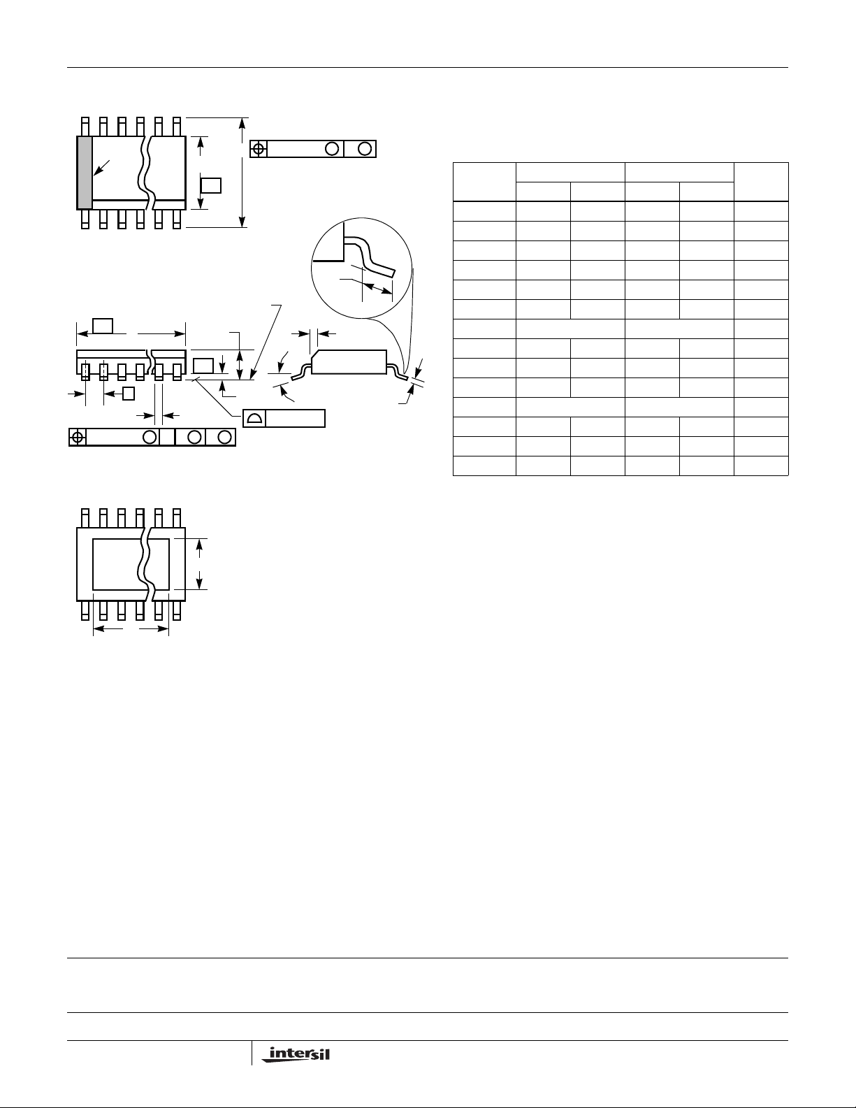
Small Outline Exposed Pad Plastic Packages (EPSOIC)
N
INDEX
AREA
123
TOP VIEW
-AD
e
B
0.25(0.010) C AM BS
SIDE VIEW
123
N
P
BOTTOM VIEW
E
H
-B-
SEATING PLANE
A
-C-
A1
M
P1
0.25(0.010) BM M
L
h x 45
α
µ
0.10(0.004)
M8.15C
8 LEAD NARROW BODY SMALL OUTLINE EXPOSED PAD
PLASTIC PACKAGE
INCHES MILLIMETERS
SYMBOL
A 0.056 0.066 1.43 1.68 -
A1 0.001 0.005 0.03 0.13 -
B 0.0138 0.0192 0.35 0.49 9
C 0.0075 0.0098 0.19 0.25 -
D 0.189 0.196 4.80 4.98 3
E 0.150 0.157 3.811 3.99 4
o
C
e 0.050 BSC 1.27 BSC -
H 0.230 0.244 5.84 6.20 -
h 0.010 0.016 0.25 0.41 5
L 0.016 0.035 0.41 0.89 6
N8 87
o
α
P - 0.126 - 3.200 11
P1 - 0.099 - 2.514 11
NOTES:
1. Symbols are defined in the “MO Series Symbol List” in Section
2.2 of Publication Number 95.
2. Dimensioning and tolerancing per ANSI Y14.5M-1982.
3. Dimension “D” does not include mold flash, protrusions or gate
burrs. Mold flash, protrusion and gate burrs shall not exceed
0.15mm (0.006 inch) per side.
4. Dimension “E” does not include interlead flash or protrusions.
Interlead flash and protrusions shall not exceed 0.25mm (0.010
inch) per side.
5. The chamfer on the body is optional. If it is not present, a visual
index feature must be located within the crosshatched area.
6. “L” is the length of terminal for soldering to a substrate.
7. “N” is the number of terminal positions.
8. Terminal numbers are shown for reference only.
9. The lead width “B”, as measured 0.36mm (0.014 inch) or greater
above the seating plane, shall not exceed a maximum value of
0.61mm (0.024 inch).
10. Controlling dimension: MILLIMETER. Converted inch
dimensions are not necessarily exact.
11. Dimensions “P” and “P1” are thermal and/or electrical enhanced
variations. Values shown are maximum size of exposed pad
within lead count and body size.
0
o
8
o
0
o
8
Rev. 0 11/03
NOTESMIN MAX MIN MAX
-
All Intersil U.S. products are manufactured, assembled and tested utilizing ISO9000 quality systems.
Intersil Corporation’s quality certifications can be viewed at www.intersil.com/design/quality
Intersil products are sold by description only. Intersil Corporation reserves the right to make changes in circuit design, software and/or specifications at any time without
notice. Accordingly, the reader is cautioned to verify that data sheets are current before placing orders. Information furnished by Intersil is believed to be accurate and
reliable. However, no responsibility is assumed by Intersil or its subsidiaries for its use; nor for any infringements of patents or other rights of third parties which may result
from its use. No license is granted by implication or otherwise under any patent or patent rights of Intersil or its subsidiaries.
For information regarding Intersil Corporation and its products, see www.intersil.com
12
FN4022.13
 Loading...