

Page 1
HIP1011D
Data Sheet November 1999
Dual PCI Hot Plug Controller
The HIP1011D is the first IC available for independent
control of two PCI Hot Plug slots. The HIP1011D has all the
features and functionality of two single PCI Hot Plug slot
controllers such as the HIP1011A but in the same foot print
area.
The HIP1011D is designed to be physically placed in close
proximity to two adjacent PCI slots servicing each
independently but reducing layoutcomplexityandplacement
costs in assembly. It creates two independent power control
solutions with discrete power MOSFETs and a few passive
components. The four supplies +5V, +3.3V, +12V, and -12V
for each slot are independently controlled. There are four
integrated current sensing switches for the +12V and -12V
and for the +5V and +3.3V supplies overcurrent protection is
provided by sensing the voltage across external currentsense resistors. In addition, on-chip references are used to
monitor the +5V, +3.3V and +12V outputs for undervoltage
conditions. The two PWRON inputs control the state of the
switches, one each for slot A and slot B outputs. During an
overcurrent condition on any output, or an undervoltage
condition on the +5V, +3.3V or +12V outputs, a LOW (0V) is
asserted on the associated FLTN output and all associated
switches are latched-off. The outputs servicing the adjacent
slot are unaffected.
File Number 4725.1
Features
• Independent Power Control of 2 PCI Slots
• Turn-Off Delay Time Adjustability
• Internal MOSFET Switches for +12V and -12V Outputs
• µP Interface for On/Off Control and Fault Reporting
• Adjustable Overcurrent Protection for All Eight Supplies
• Provides Fault Isolation
• Adjustable Turn-On Slew Rate
• Minimum Parts Count Solution
• No Charge Pump
• 100ns Response Time to Over Current
Applications
• PCI Hot-Plug
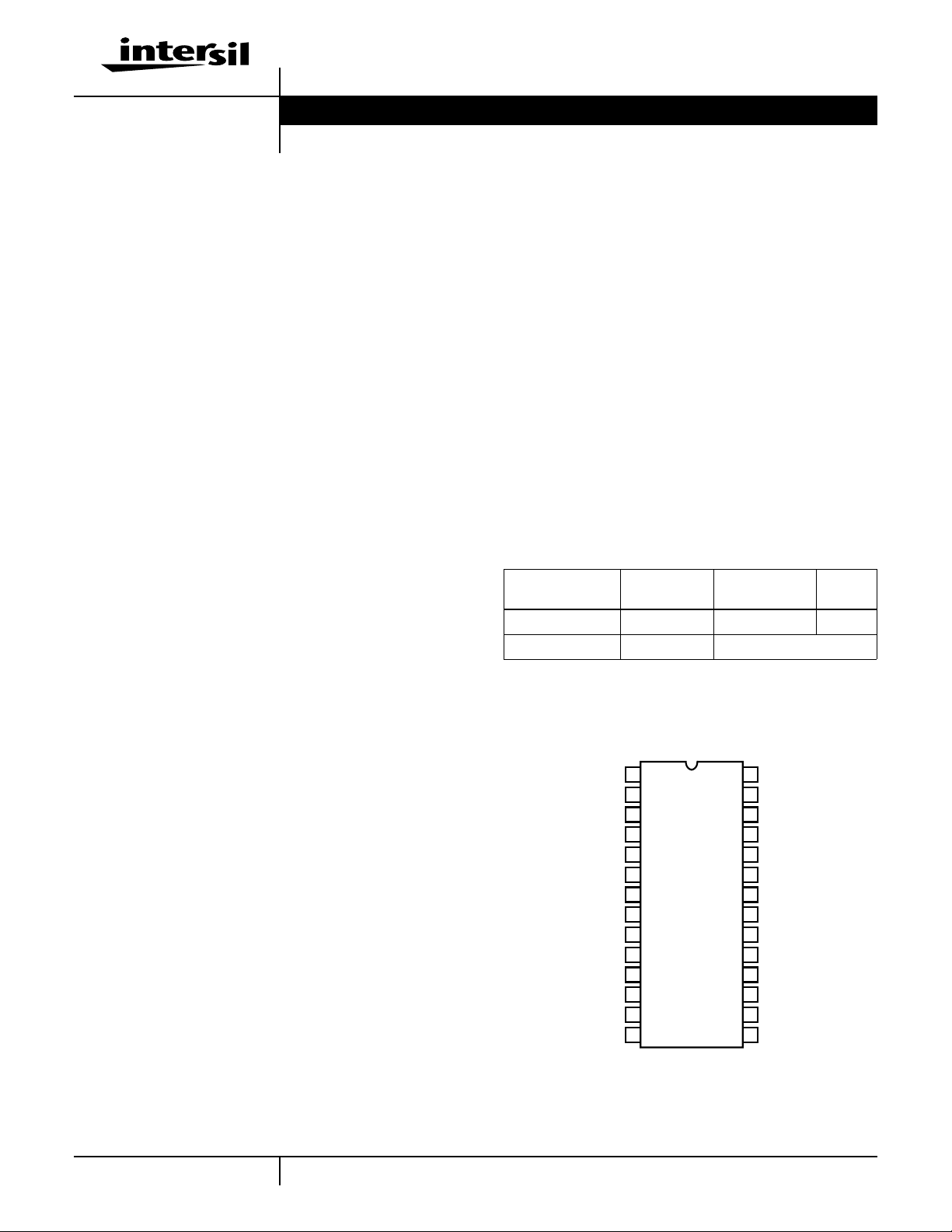
Ordering Information
TEMP.RANGE
PART NUMBER
HIP1011DCA 0 to 70 28 Ld SSOP M28.15
HIP1011DCA-T 0 to 70 Tape and Reel
(oC) PACKAGE
PKG.
NO.
The time to FLTN signal going LOW and MOSFET latch off
is user determined by a single capacitor from each FLTN pin
to ground. This added feature enables the HIP1011D to
ignore system noise transients. The FLTN latch is cleared
when the PWRON input is toggled low again. During initial
power-up of the main VCC supply (+12V), the PWRON input
is inhibited from turning on the switches,andthelatchisheld
in the Reset state until the VCC input is greater than 10V.
User programmability of the overcurrent threshold and turnon slew rate is provided. A resistor connected to the OCSET
pin programs the overcurrent threshold for both slots.
Capacitors connected to the gate pins set the turn-on rate.
Pinout
M12VO_2
M12VG_2
PWRON_2
VSS
12VG_2
12VO_2
12VO_1
12VG_1
OCSET
FLTN_1
PWRON_1
M12VG_1
M12VO_1
1
2
3
4
5
6
7
8
9
10
11
12
13
14
HIP1011D
(SSOP)
TOP VIEW
28
27
26
25
24
23
22
21
20
19
18
17
16
15
M12VIN_2
3VISEN_2
3VS_2
5VISEN_2FLTN_2
5VS_2
3V5VG_2
12VIN_2
12VIN_1
3V5VG_1
5VS_1
5VISEN_1
3VS_1
3VISEN_1
M12VIN_1
1
CAUTION: These devices are sensitive to electrostatic discharge; follow proper IC Handling Procedures.
1-888-INTERSIL or 321-724-7143
| Copyright © Intersil Corporation 1999
Page 2
Typical Application
HIP1011D
-12V BUS
+12V BUS
SYSTEM CONTROLLER
-12V12V 3.3V5V
M12VIN_1
M12G_1
C1
M12VO_1
M12VIN_2
M12G_2
C2
M12VO_2
12VIN_1
12VG_1
C3
12VO_1
12VIN_2
12VG_2
C4
12VO_2
FROM
PWRON_1
PWRON_2
OCSET
R5
SLOT 1
HIP1011D
FLTN_1VSS
OPT. OPT.
TO SYSTEM CONTROLLER
SLOT 2
5VISEN_1
3V5VG_1
3V5VG_2
5VISEN_2
3VISEN_1
3VISEN_2
FLTN_2
5VS_1
5VS_2
3VS_1
3VS_2
C5 C6
Q1
Q2
Q3
Q4
R1
R2
R3
R4
5V BUS
3.3V BUS
5V3.3V12V-12V
FIGURE 1.
2
Page 3
Simplified Schematic (1/2 HIP1011D)
SET (LOW = FAULT)
12VIN
12VIN
HIP1011D
RESET
5VREF
COMP
FAULT LATCH
+
-
LOW = FAULT
COMP
COMP
COMP
-
+
+
INHIBIT
-
+
INHIBIT
-
+
INHIBIT
12VIN
FLTN
4.6V
2.9V
10.6V
5VS
100µA
OCSET
PWRON
GND
12VIN
5V ZENER
REFERENCE
12VIN
12VIN
POWER-ON
RESET
12VIN
V
OCSET
12VIN
5VREF
LOW WHEN
12VIN < 10V
HIGH = FAULT
COMP
+
-
COMP
-
+
HIGH = SWITCHES ON
COMP
-
+
3V5VG
5VISEN
-
+
+
-
+
-
12VIN
0.3Ω
0.7Ω
3VS
3VISEN
12VIN
12VG
12VO
M12VIN
M12VG
M12VIN
FIGURE 2.
M12VO
3
Page 4

HIP1011D
Pin Descriptions
PIN NO. DESIGNATOR FUNCTION DESCRIPTION
15, 28 M12VIN -12V Input -12V Supply Input. Also provides power to the -12V overcurrent circuitry.
4, 11 FLTN Fault Output 5V CMOS Fault Output; LOW=FAULT. An optional capacitor may be place from this pin to
ground to provide additional immunity from power supply glitches.
20, 23 3V5VG 3.3V/5V Gate Output Drive the gates of the 3.3V and 5V MOSFETs. Connect a capacitor to ground to set the
start-up ramp. During turn on, this capacitor is charged with a 25µA current source.
UV comparator disabled when this pin below 9.6V nominal.
21, 22 12VIN 12V Input 12V supply input for IC and 12VO. Both 12VIns to be connected to a single +12V supply.
16, 27 3VISEN 3.3V Current Sense Connect to the load side of the currentsenseresistorinserieswithsourceofexternal 3.3V
MOSFET.
17, 26 3VS 3.3V Source Connect to source of 3.3V MOSFET. This connection along with (3VISEN) senses the
voltage drop across the sense resistor.
19, 24 5VS 5V Source Connect to source of 5V MOSFET switch. This connection along with (5VISEN) senses the
voltage drop across the sense resistor.
18, 25 5VISEN 5V Current Sense Connect to the load side of the current sense resistor in series with source of external 5V
MOSFET.
3, 12 PWRON Power On Control Controls all four switches. High to turn switches ON, Low to turn them OFF.
6, 9 12VG Gate of Internal PMOS Connect a capacitor between 12VG and 12VO to set the start-up ramp for the +12V supply.
This capacitor is charged with a 25µA current source during start-up.
UV comparator disabled when this pin >1.4Vnominal.
7, 8 12VO Switched 12V Output Switched 12V output. Rated for 0.5A.
2, 13 M12VG Gate of Internal NMOS Connect a capacitor between M12VG and M12VO to set the start-up ramp for the M12V
supply. This capacitor is charged with 25µA during start-up.
1, 14 M12VO Switched -12V
Output
10 OCSET Overcurrent Set Connect a resistor from this pin to ground to set the overcurrent trip point of all eight
5 VSS Ground Connect to common of power supplies.
Switched 12V Output. Rated for 100mA.
switches. All eight over current trips can be programmed by changing the value of this
resistor. The default (6.04kΩ, 1%) is compatible with the maximum allowable currents as
outlined in the PCI specification.
4
Page 5

HIP1011D
Absolute Maximum Ratings Thermal Information
12VIN. . . . . . . . . . . . . . . . . . . . . . . . . . . . . . . . . . . . -0.5V to +14.0V
12VO, 12VG, 3V5VG . . . . . . . . . . . . . . . . . . . .-0.5V to 12VIN +0.5V
M12VIN . . . . . . . . . . . . . . . . . . . . . . . . . . . . . . . . . . -14.0V to +0.5V
M12VO, M12VG. . . . . . . . . . . . . . . . . . . . . . V
M12VIN
-0.5V to +0.5V
3VISEN, 5VISEN . . . . . . . . . .-0.5V to the Lesser of 12VIN or +7.0V
Voltage, Any Other Pin. . . . . . . . . . . . . . . . . . . . . . . . -0.5V to +7.0V
12VO Output Current. . . . . . . . . . . . . . . . . . . . . . . . . . . . . . . . . . .3A
M12VO Output Current . . . . . . . . . . . . . . . . . . . . . . . . . . . . . . . 0.8A
ESD Classification . . . . . . . . . . . . . . . . . . . . . . . . . . . . .2KeV (HBM)
Operating Conditions
12VIN Supply Voltage Range . . . . . . . . . . . . . . . .+10.8V to +13.2V
5V and 3.3V Input Supply Tolerances. . . . . . . . . . . . . . . . . . . . . . ±10%
12VO Output Current. . . . . . . . . . . . . . . . . . . . . . . . . . . . 0 to +0.5A
M12VO Output Current . . . . . . . . . . . . . . . . . . . . . . . . . . 0 to +0.1A
Temperature Range (TA) . . . . . . . . . . . . . . . . . . . . . . . .0oC to 70oC
CAUTION: Stresses above those listed in “Absolute Maximum Ratings” may cause permanent damage to the device. This is a stress only rating and operation of the
device at these or any other conditions above those indicated in the operational sections of this specification is not implied.
NOTES:
1. θJA is measured with the component mounted on an evaluation PC board in free air.
2. All voltages are relative to GND, unless otherwise specified.
Thermal Resistance (Typical, Note 1) θJA (oC/W)
SSOP Package . . . . . . . . . . . . . . . . . . . . . . . . . . . . 95
Maximum Junction Temperature . . . . . . . . . . . . . . . . . . . . . . .150oC
Maximum Storage Temperature Range. . . . . . . . . . -65oC to 150oC
Maximum Lead Temperature (Soldering 10s) . . . . . . . . . . . . .300oC
(SSOP - Lead Tips Only)
Electrical Specifications Nominal 5.0V and 3.3V Input Supply Voltages,
12VIN = 12V, M12VIN = -12V, TA = TJ= 0 to 70oC, Unless Otherwise Specified
PARAMETER SYMBOL TEST CONDITIONS MIN TYP MAX UNITS
5V/3.3V SUPPLY CONTROL
5V Overcurrent Threshold I
5V Overcurrent Threshold Voltage V
5V Overcurrent Threshold Voltage V
5V Undervoltage Trip Threshold V
5V Undervoltage Fault Response Time t
5V Turn-On Time
OC5V
OC5V_1
OC5V_2VOCSET
5VUV
5VUV
t
ON5V
(PWRON High to 5VOUT = 4.75V)
3V Overcurrent Threshold I
3V Overcurrent Threshold Voltage V
3V Overcurrent Threshold Voltage V
3V Undervoltage Trip Threshold V
3V Undervoltage Fault Response Time t
3V5VG Undervoltage Enable Threshold
OC3V
OC3V_1
OC3V_2
3VUV
3VUV
V
3V5VGenVth
Voltage
3V Turn-On Time
t
ON3V
(PWRON High to 3VOUT = 3.00V)
3V5VG Vout High Vout_hi_35VG PWRON = High, FLTN = High 11.5 11.8 - V
Gate Output Charge Current IC
Gate Turn-On Time
3V5VG
t
ON3V5V
(PWRON High to 3V5VG = 11V)
Gate Turn-Off Time t
OFF3V5VC3V5VG
See Figure 24, Typical Application - 8 - A
V
= 0.6V 33 42 50 mV
OCSET
= 1.2V 70 80 90 mV
4.42 4.65 4.7 V
- 110 160 ns
C
3V5VG
= 0.022µF, C
= 2000µF, RL = 1Ω - 6.5 - ms
5VOUT
See Figure 24, Typical Application - 10 - A
V
V
= 0.6V 41 52 62 mV
OCSET
= 1.2V 89 98 108 mV
OCSET
2.74 2.86 2.9 V
- 110 160 ns
- 9.6 - V
C
3V5VG
= 0.022µF, C
3VOUT
= 2000µF,
- 6.5 - ms
RL = 0.43Ω
PWRON = High, V
C
= 0.033µF, 3V5VG Rising 10% to 90% - 280 - µs
3V5VG
= 4V 19 25.0 29 µA
3V+5VG
= 0.033µF, 3V5VG Falling 90% to 10% - 2 - µs
5
Page 6

HIP1011D
Electrical Specifications Nominal 5.0V and 3.3V Input Supply Voltages,
12VIN = 12V, M12VIN = -12V, TA = TJ= 0 to 70oC, Unless Otherwise Specified (Continued)
PARAMETER SYMBOL TEST CONDITIONS MIN TYP MAX UNITS
+12V SUPPLY CONTROL
On Resistance of Internal PMOS r
Overcurrent Threshold I
Overcurrent Threshold I
DS(ON)12
OC12V_1
OC12V_2
12V Undervoltage Trip Threshold V
Undervoltage Fault Response Time t
Gate Charge Current IC
Turn-On Time
t
(PWRON High to 12VG = 1V)
Turn-Off Time t
OFF12V
-12V SUPPLY CONTROL
On Resistance of Internal NMOS r
Overcurrent Threshold I
Overcurrent Threshold I
DS(ON)M12
OC12V_1
OC12V_2
Gate Output Charge Current IC
Turn-On Time
t
ONM12V
(PWRON High to M12VO = -10.8V)
Turn-Off Time t
OFFM12VCM12VG
M12VIN Input Bias Current IB
CONTROL I/O PINS
Supply Current I
OCSET Current I
Overcurrent Fault Response Time t
PWRON Threshold Voltage V
THPWRON
FLTN Output Low Voltage V
FLTN Output High Voltage V
FLTN,OHIFLTN
FLTN Output Latch Threshold V
12V Power On Enable Threshold V
12V Power On Reset Threshold V
POR,THriseVCC
POR,THfallVCC
12VUV
12VUV
12VG
ON12V
M12VG
M12VIN
VCC
OCSET
OC
FLTN,OLIFLTN
FLTN,TH
PWRON = High, ID = 0.5A, TA = TJ = 25oC - 0.3 0.35 Ω
V
V
PWRON = High, V
C
C
= 0.6V 0.6 0.75 0.9 A
OCSET
= 1.2V 1.25 1.50 1.8 A
OCSET
12VG
= 0.033µF, 12VG Falling 90% - 10% - 16 - ms
12VG
= 0.022µF, 12VG Rising 10% - 90% - 3 - µs
12VG
PWRON = High, ID = 0.1A, TA = TJ = 25oC - 0.7 1 Ω
V
V
PWRON = High, V
C
= 0.6V 0.13 0.18 0.25 A
OCSET
= 1.2V 0.23 0.38 0.52 A
OCSET
3VG
= 0.033µF, C
M12VG
= 0.033µF, M12VG Falling 90% to 10% - 3 - µs
PWRON = High - 2.5 5 mA
= 2mA - 0.5 0.7 V
= 0 to -4mA 4.0 4.3 V
FLTN High to Low transition 1.8 2.3 3 V
Voltage Rising 9.4 10 10.2 V
Voltage Falling 8.9 9.1 9.3 V
TA = TJ = 70oC - 0.35 0.50 Ω
10.25 10.6 10.8 V
- 110 - ns
= 10V 19 25.0 29 µA
TA = TJ = 70oC - 1.0 1.3 Ω
= -10V 19 25 29 µA
=50µF, RL= 120Ω -16-ms
M12VO
5.3 8 mA
93 100 107 µA
- 500 960 ns
1.0 1.6 2.1 V
6
Page 7

HIP1011D
Introduction
The HIP1011D is the first device designed to provide control
and protection of the four PCI power supplies independently
to two PCI slots. Like the widely used HIP1011 this device
complies with the PCI Hot Plug specification facilitating the
service, upgrading or expansion of PCI based servers
without the need to power down the server. The HIP1011D
protects against over current (OC) for the -12V, +12V,+3.3V,
+5V and under voltage (UV) conditions for the +12V, +3.3V,
+5V supplies.
Figure 1 illustrates the typical implementation of the
HIP1011D. Additional components for optimizing
performance for particular applications, or desired features
may be necessary.
Key Feature Description and Operation
The HIP1011D, four power MOSFETs and a few passive
components as configured in Figure 1, create a small yet
complete power control solution for two PCI slots. It provides
an OC trip level greater than the maximum PCI specified
current for each supply to each slot. Over current monitoring
and protection for the 3.3V and 5V supplies is provided by
sensing the voltage across external current-sense resistors.
For the +12V and -12V inputs, over current protection is
provided internally. On-chip references are used to monitor
the +5V, +3.3V and +12V outputs for under voltage
conditions. During an over current condition on any output,
or an under voltage condition on the +5V, +3.3V or +12V
outputs, all slot specific MOSFETs are immediately latchedoff and a LOW (0V) is presented to the appropriate FLTN
output. During initial power-up of the main V
(+12V), the
PWRON inputs are inhibited from turning on the
switches,and the latch is held in the reset state until the V
CC
supply
CC
input is greater than 10V.After a fault has been asserted and
FLTN is latched low cycling PWRON low then high will clear
the FLTN latch. User programing of the OC thresholds for
both controlled slots is provided by a single resistor
connected to the OCSET pin along with Rsense. In addition
delaytime to latch off after a fault condition can be increased
by increasing the FLTN to ground capacitance and the turnon ramp rate can be increased by increasing the gate pin
capacitance.
Customizing Circuit Performance
Over Current (OC) Set Functionality and Resistor
Choice
The HIP1011D allows easy custom programming of the over
current (OC) levels of all 4 supplies simultaneously for both
PCI slots by simply changing the resistor value between
OCSET, (pin 10), and ground. The R
OCSET 100
µA current source sets a voltage that is used in
each of eight comparators, (one for each supply for both
slots). The voltages developed across the 3.3V and 5V
sense resistors are applied to the inputs of their respective
OCSET
value and the
comparators. The +12V and -12V currents are sensed
internally with pilot devices. Once any comparator trips, that
output is fed through logic circuits resulting in the
appropriate FLTN, (pin 4 or pin 11), going low, indicating a
fault condition on that particular slot. Because of the internal
current monitoring of the +12V and -12V switches, their
programming flexibility is limited to R
OCSET
changes. The
3.3V and 5V over current trip points depend on both
R
and the value chosen for each sense resistor.
OCSET
Overcurrent design guidelines and recommendations are as
follows:
1. For PCI applications, set R
OCSET
to 6.04kΩ, and use
5mΩ 1% sense resistors (see Figure 24).
2. For non PCI specified applications, the following
precautions and limitations apply:
A. Do not exceed the maximum power of the integrated
NMOS and PMOS. High power dissipation must be
coupled with effective thermal management. The
integrated PMOS has an r
DS(ON)
of 0.3Ω. Thus, with 1A
of steady load current on each of the PMOS devices the
powerdissipation is 0.6W.The thermal impedance of the
package is 95 degrees Celsius per watt, limiting the
average DC current on the 12V supply to about 1A on
each slot and imposing an upper limit on the R
resistor. Do not use an R
resistor greater than
OCSET
OCSET
15kΩ.
The average current on the -12V supply should not
exceed 0.7A. Since the thermal restrictions on the +12V
supply are more severe,the +12V supply restricts the use
of the HIP1011 to applications where the ±12V supplies
drawrelatively little current. Since both supplies only have
one degree of freedom, the value of R
OCSET
, the flexibility
of programming is quite limited. For applications where
more power is required on the +12V supply, contact your
local Intersil sales representative for information on other
Hot Plug solutions.
B. Do not try to sense voltages across the external sense
resistors that are less than 33mV. Spurious faults due to
noise and comparator input sensitivity may result. The
minimum recommended R
value is 6kΩ. This will
OCSET
set the nominal OC voltage thresholds at 52mV and
42mV for the 3.3V and 5V comparators respectively. This
isthe voltage levelatwhich the OC fault (I
OUTxRSENSE
will occur.
C. Minimize V
RSENSE
so as to not significantly reduce the
voltage delivered to the adapter card. Remember PCB
traceand connector distribution voltage losses also need
to be considered. Make sure that the R
SENSE
resistor
can adequately handle the dissipated power. For best
resultsuse a 1%precision resistor with a lowtemperature
coefficient.
D. Minimize external FET r
DS(ON)
.Lowr
DS(ON)
or multiple
MOSFETs in parallel are recommended. See Intersil for
a complete selection of MOSFET offerings.
)
7
Page 8

HIP1011D
TABLE 1.
SUPPLY
+3.3V I
+5.0V I
+12V I
-12V I
OC
OC
OC
OC
HOW TO DETERMINE NOMINAL (±10%) I
FOR EACH SUPPLY
((100µA x R
((100µA x R
(100µA x R
(100µA x R
OCSET
OCSET
OCSET
OCSET
)/11.5)/R
)/14.5)/R
)/0.8
)/3.3
RSENSE
RSENSE
OC
Time Delay to Latch-Off
Time delay to latch-off allows for a predetermined delay from
an OC or UV event to the simultaneous latch-off of all four
supply switches of the affected slot by the HIP1011D. This
delay period is set by the capacitance value to ground from
the FLTN pins for each slot. This capacitance value tailors
the FLTN signal going low ramp rate. This provides a delay
to the fault signal latch-off threshold voltage, FLTN, Vth. By
increasing this time, the HIP1011D delays immediate latchoff of the bus supply switches, thus ignoring transient OC
and UV conditions. See additional information in the “Using
the HIP1011DEVAL1 Platform” section of this data sheet.
Caution: The primary purpose of a protection device such
as the HIP1011D is to quickly isolate a faulted card from the
voltage bus. Delaying the time to latch-off works against this
primary concern so care must be taken when using this
feature. Ensure adequate sizing of external FETs to carry
additional current during time out period. Understand that
voltage bus disruptions must be minimized for the time delay
period in the event of a crow bar failure.
Devices using an unadjustable preset delay to latch-off time
present the user with the inability to eliminate these
concerns increasing cost and the chance of additional ripple
through failures.
HIP1011D Soft Start and Turn-Off Considerations
The HIP1011D does allow the user to select the rate of ramp
up on the voltage supplies. This start-up ramp minimizes inrush current at start-up while the on card bulk capacitors
charge. The ramp is created by placing capacitors on
M12VG to M12VO, 12VG to 12VO and 3V5VG to ground.
These capacitors are each charged up by a nominal 25µA
current during turn on. The same value for all gate timing
capacitors is recommended. A recommended minimum
value of 0.033µF as a smaller value may cause overcurrent
faultsat power up.This recommendation results in a nominal
gate voltage ramp rate of 0.76V/ms. The gate capacitors
must be discharged when a fault is detected to turn off the
powerFETs. Thus, larger caps slow the response time. If the
gate capacitors are too large the HIP1011D may not be able
to adequately protect the bus or the power FETs. The
HIP1011D has internal discharge FETs to discharge the
load when disabled. Upon turn-off these internal switches on
each output discharge the load capacitance pulling the
output to gnd. These switches are also on when PWRON is
low thus an open slot is held at the gnd level.
Decoupling Precautions and Recommendations
For the HIP1011D proper decoupling is a particular concern
during the normal switching operation and especially during
a card crowbar failure. If a card experiences a crow bar short
to ground, the supply to the other card will experience
transients until the faulted card is isolated from the bus. In
addition the common IC nodes between the two sides can
fluctuate unpredictably resulting in a false latch-off of the
second slot. Additionally to the mother board bulk
capacitance, it is recommended that 10µF capacitors be
placed on both the +12V and -12V lines of the HIP1011D as
close to the chip as possible.
Recommended PCB Layout Design Best Practices
To ensure accurate current sensing, PCB traces that
connect each of the current sense resistors to the HIP1011D
must not carry any load current. This can be accomplished
by two dedicated PCB kelvin traces directly from the sense
resistors to the HIP1011D, see examples of correct and
incorrect layouts below in Figure 3. To reduce parasitic
inductance and resistance effects, maximize the width of the
high-current PCB traces.
CORRECT
TO HIP1011D
VS AND VISEN
SENSE RESISTOR
FIGURE 3. SENSE RESISTOR PCB LAYOUT
INCORRECT
TO HIP1011D
VS AND VISEN
CURRENT
8
Page 9

Typical Performance Curves
HIP1011D
340
320
+12 (mΩ)
300
ON
PMOS r
280
260
0 5 10 15 20 25 30 35 40 45 50 55 60 65 70
NMOS -12 r
ON
PMOS +12 r
TEMPERATURE (oC)
ON
FIGURE 4. rON vs TEMPERATURE FIGURE 5. UV TRIP vs TEMPERATURE
10.59
10.57
1000
900
800
700
600
-12 (mΩ)
ON
NMOS r
4.632
4.631
4.630
4.629
5V UVTRIP (V)
4.628
4.627
4.626
0 5 10 15 20 25 30 35 40 45 50 55 60 65 70
TEMPERATURE (oC)
100
3V OCVth, VOCSET = 1.2V
85
70
5 UV
3.3 UV
5V OCVth, VOCSET = 1.2V
2.862
2.861
2.860
3.3V UVTRIP (V)
2.859
2.858
12 UV TRIP (V)
10.55
10.53
0 5 10 15 20 25 30 35 40 45 50 55 60 65 70
TEMPERATURE (oC)
OC Vth (mV)
3V OCVth, VOCSET = 0.6V
55
40
0 5 10 15 20 25 30 35 40 45 50 55 60 65 70
TEMPERATURE (oC)
FIGURE 6. 12 UV TRIP vs TEMPERATURE FIGURE 7. OC Vth vs TEMPERATURE
6
+12V BIAS
5
4
-12V BIAS
3
ABS +/-12V BIAS (MA)
2
0 5 10 15 20 25 30 35 40 45 50 55 60 65 70
TEMPERATURE (oC)
10.0
9.75
9.5
9.25
+12V THRESHOLDS (V)
+12V POWER ON RESET
9.0
0 5 10 15 20 25 30 35 40 45 50 55 60 65 70
TEMPERATURE (oC)
5V OCVth, VOCSET = 0.6V
+12V POWER ON ENABLE
FIGURE 8. BIAS CURRENT vs TEMPERATURE FIGURE 9. 12V ENABLE AND RESET THRESHOLD
VOLTAGES vs TEMPERATURE
9
Page 10

Typical Performance Curves (Continued)
HIP1011D
1.5
1.25
1.0
0.75
+12V OVER CURRENT (A)
0.5
0 5 10 15 20 25 30 35 40 45 50 55 60 65 70
VOCSET = 1.2V
VOCSET = 0.6V
TEMPERATURE (
o
C)
0.4
VOCSET = 1.2V
0.3
0.2
VOCSET = 0.6V
0.1
-12V OVER CURRENT (A)
0
0 5 10 15 20 25 30 35 40 45 50 55 60 65 70
TEMPERATURE (
o
C)
FIGURE 10. +12V OVER CURRENT LEVEL vs TEMPERATURE FIGURE 11. -12V OVER CURRENT vs TEMPERATURE
102
101
100
2.4
2.35
2.3
IOC SET (µA)
99
98
0 5 10 15 20 25 30 35 40 45 50 55 60 65 70
TEMPERATURE (oC)
2.25
FLTN LATCH OFF THRESHOLD (V)
2.2
0 5 10 15 20 25 30 35 40 45 50 55 60 65 70
TEMPERATURE (
o
C)
FIGURE 12. OCSET CURRENT vs TEMPERATURE FIGURE 13. FLTNLATCH-OFF THRESHOLD VOLTAGE vs
TEMPERATURE
100
90
80
70
OV / UV TO FAULT RESPONSE TIME (ns)
60
0 5 10 15 20 25 30 35 40 45 50 55 60 65 70
TEMPERATURE (
o
C)
FIGURE 14. OVER CURRENT AND UNDERVOLTAGE TO FLTN RESPONSE TIME vs TEMPERATURE
10
Page 11

HIP1011D
Using the HIP1011DEVAL1 Platform
General and Biasing Information
The HIP1011DEVAL1platform (Figure 24) comes as a three
part set consisting of 1 mother board emulator and 2 load
cards. This evaluationplatform allows a designer to evaluate
and modify the performance and functionality of the
HIP1011D in a simple environment.
Test point numbers (TP#) correspond to the HIP1011D
device (U5) pin numbers thus TP3 and TP12 are PWRON_2
and PWRON_1 respectively.These 2 pins are the HIP1011D
control inputs for each of the 2 integrated but independent
PCI power controllers in the HIP1011D.
On the HIP1011DEVAL1 platform are 4 HUF76132SK8,
(11.5mΩ, 30V, 11.5A) N-Channel power MOSFETs, (Q1-
Q4) these are used as the external switches for the +5V and
+3.3V supplies to the load card connectors, P1 and P2.
Current sensing is facilitated by the four 5mΩ 1W metal strip
resistors (R1-R4), the voltages developed across the sense
resistors are compared to references on board the
HIP1011D.
The HIP1011DEVAL1 platform is powered through the J1 to
J5 connector jacks near the top of the board, see Table 2 for
bias voltage assignments.
TABLE 2. HIP1011DEVAL1 BIAS ASSIGNMENTS
J1 J2 J3 J4 J5
GND +5V -12V +12V +3.3V
Evaluating Time Delay to Latch-Off
Provided for delay to latch-off evaluation are 2 locations for
1206 SMD capacitors, C7 and C8. Filling these locations
places a capacitor to ground from each of the HIP1011D
FLTN pins thus tailoring the FLTN signal going low ramp
rate. This provides a delay to the fault signal latch-off
threshold voltage, FLTN Vth. By increasing this time the
HIP1011D delays immediate latch-off of the bus supply
switches,thus ignoring transient OC and UV conditions. See
Table 3 illustrating the time it takes for switch gate turn-off
from the FLTN start of response to an OC or UV condition.
The FLTN response to an OC or UV condition is 110ns. See
Figures 20 through 23 for waveforms.
The intent of any protection device is to isolate the supply
quickly so a faulty card does not drag down a supply. A
longer latch-off delay results in less isolation from a faulty
card to supply.
TABLE 3.
C7 AND C8 VALUE OPEN 0.001µF 0.01µF 0.1µF
FLTN to Gate Response 0.1µs 0.44µs 2.9µs28µs
FLTN
3V5VG
FLTN, Vth
After properly biasing the HIP1011D and ensuring there is
an adequate ground return from the HIP1011DEVAL1
platform to the power supplies, (otherwise anomalous and
unpredictable results will occur) signal the PWRON inputs
low then insert the load cards as shown in Figure 15.
Signaling either or both PWRON pins high (>2.4V) will turn
on the appropriate FET switches and apply voltage to the
load cards.
LOAD CARDS
HIP1011D
FIGURE 16. TIMING DIAGRAM
10ms
1ms
100µs
10µs
1µs
100ns
10ns
1ns
0.001µF 0.1µF1µF10µFOPEN 0.01µF
FIGURE 17. TYPICAL OC/UV TO VG RESPONSE vs FLTN CAP
FIGURE 15. cORRECT INSTALLATION OF LOAD CARDS
11
Page 12

Typical Performance Curves (Continued)
HIP1011D
SUPPLY CURRENT
SUPPLY CURRENT
CH2
CH1
CH1 AND CH2 VOLTAGE (5V/DIV) TIME (100ms/DIV)
CH3 CURRENT (2A/DIV)
ENABLE 2
ENABLE 1
FIGURE 18. HIP1011DEVAL13.3V SUPPLYCURRENT AS
EACH SLOT CONTROLLER TURNS ON INTO
LOAD CARD
VG
CH3
CH2
CH1
ENABLE 1
CH1 AND CH2 VOLTAGE (5V / DIV) TIME (100ms/DIV)
CH3 CURRENT (2A/DIV)
ENABLE 2
FIGURE 19. HIP1011DEVAL13.3V SUPPLYCURRENT AS
CONTROLLER 1 TURNS ON INTO SHORTED
LOAD CARD
VG
FLTN
FLTN
VOLTAGE (2V/DIV)
TIME (1µs /DIV)
FLTN = OPEN
FIGURE 20. FLTN TO 35VG DELAY FIGURE 21. FLTN TO 35VG DELAY
VG
FLTN
VOLTAGE (2V/DIV) TIME (2µs/DIV)
FLTN = 0.01µF
FIGURE 22. FLTN TO 35VG DELAY FIGURE 23. FLTN TO 35VG DELAY
VOLTAGE (2V/DIV) TIME (1µs /DIV)
FLTN = 0.001µF
VG
FLTN
VOLTAGE (2V/DIV) TIME (10µs/DIV)
FLTN = 0.1µF
12
Page 13

HIP1011D
J3
-12V BUS
J1
J4
+12V BUS
12V -12V 5V
M12VIN_1
M12G_1
C1
M12VO_1
M12VIN_2
M12G_2
C2
M12VO_2
TP3
TP12
C3
C4
12VIN_1
12VG_1
12VO_1
12VIN_2
12VG_2
12VO_2
PWRON_1
PWRON_2
OCSET
R5
HIP1011D
U1
P1
5VISEN_1
5VS_1
3V5VG_1
3V5VG_2
5VS_2
5VISEN_2
3VISEN_1
3VS_1
3VS_2
FLTN_1VSS
R6
3VISEN_2
FLTN_2
R7
C7
No Pop
Q1
Q2
Q3
Q4
R1
R2
R3
R4
5V BUS
3.3V BUS
C8
No Pop
3.3V
TP11
TP4
C5
J2
C6
J5
P2
FIGURE 24.
D1
D2
5v3.3v-12v 12v
13
Page 14

HIP1011D
TABLE 4. HIP1011DEVAL1 BOARD COMPONENT LISTING
COMPONENT
DESIGNATOR COMPONENT NAME COMPONENT DESCRIPTION
U1 HIP1011DCB PCI HotPlug Controller Intersil, HIP1011DCB Dual PCI HotPlug Controller
Q1, Q2, Q3, Q4 HUF76132SK8 Intersil, HUF76132SK8, 11.5mΩ, 30V, 11.5A Logic Level N-Channel
MOSFET
R1 - R4 Sense Resistor for 3.3V and 5V Supplies Dale, WSL-2512 5mΩ Metal Strip Resistor
C1 - C6 Gate Timing Capacitors 0.033µF 805 Chip Capacitor
R5 Over Current Set Resistor 6kΩ 805 Chip Resistor
C7, C8 (Not Provided) Latch-Off Delay Capacitors Place provided for 805 Chip Cap
R6, R7 LED Series Resistors 470Ω 805 Chip Resistors
D1, D2 Fault Indicating LED Green SMD LED
TP1 - TP28 Test Point for Corresponding Device Pin Number
P1, P2 Connectors for Load Cards Sullins EZM06DRXH
RL1 3.3V Load Board Resistor 1.1Ω, 10W
RL2 5.0V Load Board Resistor 2.5Ω, 10W
RL3 +12V Load Board Resistor 47Ω, 5W
RL4 -12V Load Board Resistor 240Ω, 2W
CL1, CL2 +3.3V and +5.0V Load Board Capacitors 2200µF
CL3, CL4 +12V and -12V Load Board Capacitors 100µF
3.3V
5.0V
+12V
-12V
RL1
CL1
RL2
CL2
RL3
CL3
RL4
CL4
FIGURE 25. LOAD BOARD (2x)
14
Page 15

HIP1011D
Shrink Small Outline Plastic Packages (SSOP)
N
INDEX
AREA
123
-A-
E
-B-
SEATING PLANE
D
A
-C-
0.25(0.010) BM M
H
GAUGE
PLANE
0.25
0.010
h x 45
L
o
α
e
B
0.17(0.007) C AM BS
M
A1
0.10(0.004)
NOTES:
1. Symbols are defined in the “MO Series Symbol List” in Section 2.2
of Publication Number 95.
2. Dimensioning and tolerancing per ANSI Y14.5M-1982.
3. Dimension “D” does not include mold flash, protrusions or gate
burrs. Mold flash, protrusion and gate burrs shall not exceed
0.15mm (0.006 inch) per side.
4. Dimension “E” does not include interlead flash or protrusions. Interlead flash and protrusions shall not exceed 0.25mm (0.010 inch)
per side.
5. The chamfer on the body is optional. If it is not present, a visual index feature must be located within the crosshatched area.
6. “L” is the length of terminal for soldering to a substrate.
7. “N” is the number of terminal positions.
8. Terminal numbers are shown for reference only.
9. Dimension “B” does not include dambar protrusion. Allowable dambar protrusion shall be 0.10mm (0.004 inch) total in excess of “B”
dimension at maximum material condition.
10. Controllingdimension: INCHES. Converted millimeter dimensions
are not necessarily exact.
A2
C
M28.15
28 LEAD SHRINK NARROW BODY SMALL OUTLINE
PLASTIC PACKAGE
INCHES MILLIMETERS
SYMBOL
A 0.053 0.069 1.35 1.75 A1 0.004 0.010 0.10 0.25 A2 - 0.061 - 1.54 -
B 0.008 0.012 0.20 0.30 9
C 0.007 0.010 0.18 0.25 -
D 0.386 0.394 9.81 10.00 3
E 0.150 0.157 3.81 3.98 4
e 0.025 BSC 0.635 BSC -
H 0.228 0.244 5.80 6.19 -
h 0.0099 0.0196 0.26 0.49 5
L 0.016 0.050 0.41 1.27 6
N28 287
o
α
0
o
8
o
0
o
8
NOTESMIN MAX MIN MAX
-
Rev. 0 2/95
All Intersil semiconductor products are manufactured, assembled and tested under ISO9000 quality systems certification.
Intersil semiconductor products are sold by description only. Intersil Corporation reserves the right to make changes in circuit design and/or specifications at any time without notice. Accordingly, the reader is cautioned to verify that data sheets are current before placing orders. Information furnished by Intersil is believed to be accurate and
reliable. However, no responsibility is assumed by Intersil or its subsidiaries for its use; nor for any infringements of patents or other rights of third parties which may result
from its use. No license is granted by implication or otherwise under any patent or patent rights of Intersil or its subsidiaries.
For information regarding Intersil Corporation and its products, see web site www.intersil.com
Sales Office Headquarters
NORTH AMERICA
Intersil Corporation
P. O. Box 883, Mail Stop 53-204
Melbourne, FL 32902
TEL: (321) 724-7000
FAX: (321) 724-7240
15
EUROPE
Intersil SA
Mercure Center
100, Rue de la Fusee
1130 Brussels, Belgium
TEL: (32) 2.724.2111
FAX: (32) 2.724.22.05
ASIA
Intersil (Taiwan) Ltd.
7F-6, No. 101 Fu Hsing North Road
Taipei, Taiwan
Republic of China
TEL: (886) 2 2716 9310
FAX: (886) 2 2715 3029
 Loading...