

Page 1
HIP1011B
Data Sheet March 2000
PCI Hot Plug Controller
The HIP1011B, the third product in the HIP1011 family, is an
electronic circuit breaker that monitors, reports and protects
circuits from excessive load currents. As a pin-for-pindrop-in
alternative offering similar functionality to the widely used
HIP1011, the HIP1011B is compatible with CompactPCI
peripheral boards and PCI Hot Plug systems where voltage
“health” monitoring and reporting are centralized by the
system controller IC. The HIP1011B does not monitor nor
respond to under voltage conditions thus making control of a
wide range of voltages possible.
The HIP1011B creates a small and simple yet complete
power control solution to control the four independent
supplies (+5V, +3.3V, +12V, and -12V) found in PCI and
CompactPCI systems. For the +12V and -12V supplies,
overcurrent protection is provided internally with integrated
current sensing FET switches. For the +5V and +3.3V
supplies, overcurrent protection is provided by sensing the
voltage across the external current-sense resistors. The
PWRON input controls the state of both internal and external
switches. During an overcurrent condition on any output, all
MOSFETs are latched-off and a LOW (0V) is asserted on
the FLTN output. The FLTN latch is cleared when the
PWRONinput is toggled low again. During initial power-up of
the main V
from turning on the switches, and the latch is held in the
Reset state until the V
User programmability of the overcurrent threshold, response
time and turn-on slew rate is provided. A resistor connected
to the OCSET pin programs the overcurrent thresholds. A
capacitor may be added to the FLTN pin to adjust the fault
reporting and power-supply latch-off response times after an
over-current event. Capacitors connected to the gate pins
determine the turn-on rate.
supply (+12V), the PWRON input is inhibited
CC
input is greater than 10V.
CC
File Number 4640.3
Features
• Allows for System Centralized Voltage Monitoring
• Adjustable Delay to Fault Notification and Latch-Off
• Controls Four Supplies: +5V, +3.3V, +12V, and -12V
• Internal MOSFET Switches for +12V and -12V Outputs
• µP Interface for On/Off Control and Fault Reporting
• Adjustable Overcurrent Protection for All Supplies
• Provides Overcurrent Fault Isolation
• Adjustable Turn-On Slew Rate
• Minimum Parts Count Solution
• No Charge Pump
Applications
• PCI Hot Plug
CompactPCI
•
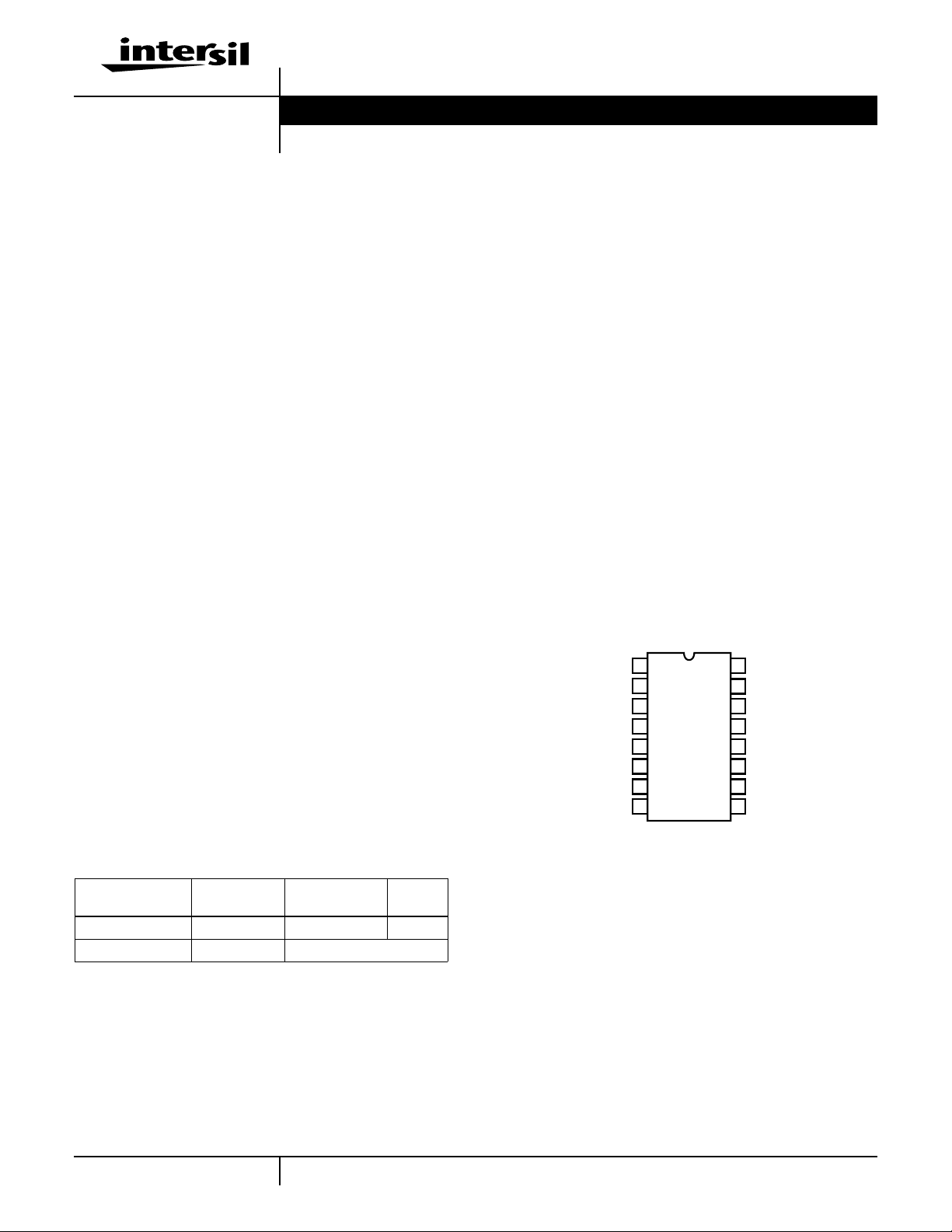
Pinout
HIP1011B
(SOIC)
TOP VIEW
M12VIN
FLTN
3V5VG
V
CC
12VIN
3VISEN
3VS
OCSET
1
2
3
4
5
6
7
8
16
15
14
13
12
11
10
9
M12VO
M12VG
12VG
GND
12VO
5VISEN
5VS
PWRON
Ordering Information
TEMP.RANGE
PART NUMBER
HIP1011BCB 0 to 70 16 Ld SOIC M16.15
HIP1011BCB-T 0 to 70 Tape and Reel
(oC) PACKAGE
1
PKG.
NO.
CAUTION: These devices are sensitive to electrostatic discharge; follow proper IC Handling Procedures.
1-888-INTERSIL or 321-724-7143
| Copyright © Intersil Corporation 2000
Page 2
Typical Application
3.3V INPUT
-12V INPUT
12V INPUT
POWER CONTROL INPUT
FAULT OUTPUT (ACTIVE LOW)
Simplified Schematic
3.3V,
7.6A OUT
5mΩ, 1%
6.04kΩ
1%
SET (LOW = FAULT)
HIP1011B
12V,
0.5A OUT 0.1A OUT 5A OUT
HIP1011B
M12VIN
FLTN
3V5VG
V
12V
3VISEN
3VS
OCSET
M12VO
M12VG
CC
IN
5VISEN
PWRON
(OPTIONAL)
12VG
GND
12VO
5VS
V
CC
FAULT LATCH
5V,-12V,
0.033µF
0.033µF
NOTE:
ALL CAPACITORS ARE ±10%.
5mΩ, 1%
5V INPUT
HUF761315K8
0.033µF
LOW = FAULT
FLTN
V
CC
100µA
OCSET
PWRON
GND
V
V
CC
5V ZENER
REFERENCE
V
CC
12VIN
POWER-ON
RESET
V
CC
V
V
CC
5V
REF
LOW WHEN VCC < 10V
OCSET
CC
HIGH =
FAULT
RESET
COMP
COMP
COMP
HIGH = SWITCHES ON
COMP
V
OCSET
V
+
-
V
OCSET
+
-
V
OCSET
-
+
+
-
/3.3
OCSET
-
-
+
-
+
-
/13.3
/0.8
/17
+
V
CC
+
V
CC
0.3Ω
5VS
3V5VG
5VISEN
3VS
3VISEN
12VIN
12VG
12VO
M12VO
M12VG
0.7Ω
M12VIN
2
Page 3

HIP1011B
Pin Descriptions
PIN DESIGNATOR FUNCTION DESCRIPTION
1 M12VIN -12V Input -12V Supply Input. Also provides power to the -12V overcurrent circuitry.
2 FLTN Fault Output 5V CMOS Fault Output; LOW = FAULT. A capacitor may be placed from this pin to ground to
provide delay time to fault notification and power supply latch-off.
3 3V5VG 3.3V/5V Gate
Output
4VCC12V VCC Input Connect to unswitched 12V supply.
5 12V
6 3VISEN 3.3V Current Sense Connect to the load side of the current sense resistor in series with source of external 3.3V
7 3VS 3.3V Source Connect to Source of 3.3V MOSFET. This connection along with pin 6 (3VISEN) senses the
8 OCSET Overcurrent Set Connect a resistor from this pin to ground to set the overcurrent trip point of all four switches. All
9 PWRON Power On Control Controls all Four Switches. High to Turn Switches ON, Low to turn them OFF.
10 5VS 5V Source Connectto Source of 5V MOSFET Switch. This connection along with pin 11 (5VISEN) senses
11 5VISEN 5V Current Sense Connectto the load side ofthe current sense resistor in serieswith source of external 5V MOSFET.
12 12VO Switched 12V
13 GND Ground Connect to common of power supplies.
14 12VG Gate of Internal
15 M12VG Gate of Internal
16 M12VO Switched -12V
IN
12V Input Switched 12V supply input.
Output
PMOS
NMOS
Output
Drive the Gates of the 3.3V and 5V MOSFETs. Connect a capacitor to ground to set the startup ramp. During turn on, this capacitor is charged with a 25µA current source.
MOSFET. This pin tied to GND when FET switch outputs disabled.
voltage drop across the sense resistor.
four over current trips can be programmed by changing the value of this resistor. The default
(6.04kΩ, 1%) is compatible with the maximum allowable currents as outlined in the PCI
specification.
the voltage drop across the sense resistor.
This pin tied to GND when FET switch outputs disabled.
Switched 12V output. This pin tied to GND when FET switch outputs disabled.
Connect a capacitor between 12VG and 12VO to set the start up ramp for the +12V supply.
This capacitor is charged with a 25µA current source during start-up.
Connect a capacitor between M12VG and M12VO to set the start-up ramp for the M12V
supply. This capacitor is charged with 25µA during start-up.
Switched 12V Output. This pin tied to GND when FET switch outputs disabled.
3
Page 4

HIP1011B
Absolute Maximum Ratings Thermal Information
VCC, 12VIN . . . . . . . . . . . . . . . . . . . . . . . . . . . . . . . -0.5V to +14.0V
12VO . . . . . . . . . . . . . . . . . . . . . . . . . . . . . . -0.5V to V12VIN+ 0.5V
12VO, 12VG, 3V5VG . . . . . . . . . . . . . . . . . . . . -0.5V to VCC+ 0.5V
M12VIN . . . . . . . . . . . . . . . . . . . . . . . . . . . . . . . . . -15.0V to + 0.5V
M12VO, M12VG. . . . . . . . . . . . . . . . . . . . . V
M12VIN
-0.5V to + 0.5V
3VISEN, 5VISEN . . . . . . . . . . . -0.5V to the lesser of VCC or + 7.0V
Voltage, Any Other Pin. . . . . . . . . . . . . . . . . . . . . . . -0.5V to + 7.0V
12VO Output Current. . . . . . . . . . . . . . . . . . . . . . . . . . . . . . . . . . 3A
M12VO Output Current . . . . . . . . . . . . . . . . . . . . . . . . . . . . . . . 0.8A
ESD Classification . . . . . . . . . . . . . . . . . . . . . . . . . . . . 4KeV (HBM)
Operating Conditions
VCC Supply Voltage Range. . . . . . . . . . . . . . . . . +10.8V to +13.2V
12VO Output Current. . . . . . . . . . . . . . . . . . . . . . . . . . . . 0 to +0.5A
M12VO Output Current . . . . . . . . . . . . . . . . . . . . . . . . . . 0 to +0.1A
Temperature Range (TA) . . . . . . . . . . . . . . . . . . . . . . . 0oC to 70oC
CAUTION: Stresses above those listed in “Absolute Maximum Ratings” may cause permanent damage to the device. This is a stress only rating and operation of the
device at these or any other conditions above those indicated in the operational sections of this specification is not implied.
NOTES:
1. θJA is measured with the component mounted on a low effective thermal conductivity test board in free air. See Tech Brief 379 for details.
2. All voltages are relative to GND, unless otherwise specified.
Thermal Resistance (Typical, Note 1) θJA (oC/W)
SOIC Package . . . . . . . . . . . . . . . . . . . . . . . . . . . . . 105
Maximum Junction Temperature . . . . . . . . . . . . . . . . . . . . . . 125oC
Maximum Storage Temperature Range. . . . . . . . . . -65oC to 150oC
Maximum Lead Temperature (Soldering 10s) . . . . . . . . . . . . 300oC
(SOIC - Lead Tips Only)
Die Characteristics
Number of Transistors . . . . . . . . . . . . . . . . . . . . . . . . . . . . . . . . 250
Electrical Specifications Nominal 5V and 3.3V Input Supply Voltages,
VCC = 12VIN = 12V, M12VIN = -12V, TA = TJ= 0 to 70oC, Unless Otherwise Specified
PARAMETER SYMBOL TEST CONDITIONS MIN TYP MAX UNITS
5V/3.3V SUPPLY CONTROL
5V Overcurrent Threshold I
5V Overcurrent Threshold Voltage V
5V Overcurrent Threshold Voltage V
5V Turn-On Time
OC5V_1
OC5V_2
t
(PWRON High to 5VOUT = 4.75V)
5VS Input Bias Current IB
5VISEN Input Bias Current IB
3V Overcurrent Threshold I
3V Overcurrent Threshold Voltage V
3V Overcurrent Threshold Voltage V
3V Turn-On Time
OC3V_1
OC3V_2
t
(PWRON High to 3VOUT = 3.00V)
3VS Input Bias Current IB
3VISEN Input Bias Current IB
3V5VG V
High V
OUT
OUT_HI_35VG
Gate Output Charge Current IC
Gate Turn-On Time
t
ON3V5V
(PWRON High to 3V5VG = 11V)
OC5V
ON5V
5VS
5VISEN
OC3V
ON3V
3VS
3VISEN
3V5VG
See Figure 1, Typical Application - 8 - A
V
= 0.6V 30 36 42 mV
OCSET
V
= 1.2V 66 72 79 mV
OCSET
C
= 0.022µF, C
3V5VG
5VOUT
RL = 1Ω
PWRON = High -40 -26 -20 µA
PWRON = High -160 -140 -110 µA
See Figure 1, Typical Application 10 A
V
= 0.6V 42 49 56 mV
OCSET
V
= 1.2V 88 95 102 mV
OCSET
C
= 0.022µF, C
3V5VG
3VOUT
RL = 0.43Ω
PWRON = High -40 -26 -20 µA
PWRON = High -160 -140 -110 µA
3V5VG IOUT = 5µΑ 11 11.7 - V
PWRON = High, V
C
= 0.1µF - 280 500 µs
3V5VG
3V5VG
= 2000µF,
= 2000µF,
- 6.5 - ms
- 6.5 - ms
= 2V 22.5 25.0 27.5 µA
Gate Turn-Off Time t
OFF3V5V
Gate Turn-Off Time C
4
C
= 0.1µF, 3V5VG from 9.5V to 1V - 13 17 µs
3V5VG
= 0.022µF, 3V5VG Falling 90% to 10% - 2 - µs
3V5VG
Page 5

HIP1011B
Electrical Specifications Nominal 5V and 3.3V Input Supply Voltages,
VCC = 12VIN = 12V, M12VIN = -12V, TA = TJ= 0 to 70oC, Unless Otherwise Specified (Continued)
PARAMETER SYMBOL TEST CONDITIONS MIN TYP MAX UNITS
+12V SUPPLY CONTROL
On Resistance of Internal PMOS r
Overcurrent Threshold I
Overcurrent Threshold I
Gate Charge Current IC
Turn-On Time (PWRON High to
DS(ON)12
OC12V_1
OC12V_2
12VG
t
ON12V
12VG = 1V)
Turn-Off Time t
OFF12V
Turn-Off Time C
-12V SUPPLY CONTROL
On Resistance of Internal NMOS r
Overcurrent Threshold I
Overcurrent Threshold I
Gate Output Charge Current IC
Turn-On Time (PWRON High to
DS(ON)M12
OC12V_1
OC12V_2
M12VG
t
ONM12V
M12VG = -1V)
Turn-On Time (PWRON High to
t
ONM12V
M12VO = -10.8V)
Turn-Off Time t
OFFM12V
Turn-Off Time C
M12VIN Input Bias Current IB
M12VIN
CONTROL I/O PINS
PWRON = High, ID = 0.5A, TA = TJ = 25oC 0.18 0.3 0.35 Ω
V
= 0.6V 0.6 0.75 0.9 A
OCSET
V
= 1.2V 1.25 1.50 1.8 A
OCSET
PWRON = High, V
C
= 0.022µF - 16 20 ms
12VG
C
= 0.1µF, 12VG - 9 12 µs
12VG
= 0.022µF, 12VG Rising 10% - 90% - 3 - µs
12VG
= 3V 22.5 25 28.5 µA
12VG
PWRON = High, ID = 0.1A, TA = TJ = 25oC 0.5 0.7 0.9 Ω
V
= 0.6V 0.15 0.18 0.25 A
OCSET
V
= 1.2V 0.30 0.37 0.50 A
OCSET
PWRON = High, V
C
= 0.022µF - 160 300 µs
M12VG
C
= 0.022µF, C
M12VG
C
= 0.1µF, M12VG - 18 23 µs
M12VG
= 0.022µF, M12VG Falling 90% to 10% - 3 - µs
M12VG
= -4V 22.5 25 28.5 µA
3VG
= 50µF, RL = 120Ω -16-ms
M12VO
PWRON = High - 2 2.6 mA
Supply Current I
OCSET Current I
Overcurrent Fault Response Time t
PWRON Threshold Voltage V
THPWRON
FLTN Output Low Voltage V
FLTN Output High Voltage V
FLTN Output Latch Threshold V
FLTN,OHIFLTN
FLTN,TH
12V Power On Reset Threshold V
5
VCC
OCSET
OC
FLTN,OLIFLTN
POR,TH
VCC Voltage Falling 8.7 9.4 9.9 V
4 5 5.8 mA
95 100 105 µA
- 500 960 ns
0.8 1.6 2.1 V
= 2mA - 0.6 0.9 V
= 0 to -4mA 3.9 4.3 4.9 V
1.45 1.8 2.25 V
Page 6

Typical Performance Curves
HIP1011B
340
320
+ 12 (mΩ)
300
ON
PMOS r
280
260
0 5 10 15 20 25 30 35 40 45 50 55 60 65 70
NMOS -12 r
TEMPERATURE (oC)
ON
PMOS +12 r
ON
FIGURE 1. rON vs TEMPERATURE FIGURE 2. OC VTH vs TEMPERATURE (VR
102
101
100
I OCSET (µA)
99
1000
900
800
700
600
-12 (mΩ)
ON
NMOS r
105
95
85
OC VTH (mV)
75
65
0 5 10 15 20 25 30 35 40 45 50 55 60 65 70
9.5
9.4
9.3
VTH (V)
POR
V
9.2
3V OCVTH
5V OCVTH
TEMPERATURE (oC)
OCSET
= 1.21V)
98
0 5 10 15 20 25 30 35 40 45 50 55 60 65 70
TEMPERATURE (oC)
9.1
0 5 10 15 20 25 30 35 40 45 50 55 60 65 70
TEMPERATURE (oC)
FIGURE 3. OCSET CURRENT vs TEMPERATURE FIGURE 4. VCC POWER ON RESET VTH vs TEMPERATURE
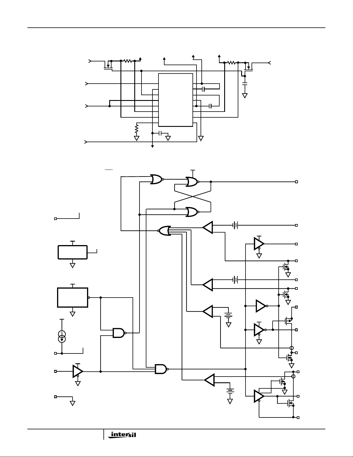
Adjusting the Fault Reporting and Power
Supply Latch-Off Delay Times
Figure 5 illustrates the relationship between the FLTN signal
and the gate drive outputs. Duration
between FLTN starting to transition from High to Low,
(indicating a fault has occurred) and the start of the gate
drive outputs latching off. The latch-off is initiated by the
falling FLTN signal reaching the output latch threshold
voltage, VFLTN, TH. For additional details and wave forms
see HIP1011A Data Sheet FN4631. Table 1 illustrates the
effect of the FLTN capacitor on the response times.
TABLE 1. RESPONSE TIME TABLE
3V5VG Response a 0.85µs37µs 3.8ms
a, indicates the time
0.001µF 0.1µF10µF
a
T1 T2
FIGURE 5. TIMING DIAGRAM
V
FLTN,TH
FLTN
3V5VG
6
Page 7

HIP1011B
Applications
Implementing the HIP1011B in the CompactPCI
Hot Swap Application
This application offers to the CompactPCI peripheral board
designer programmable Over Current (OC) protection,
programmabledelays to latch off, and soft start ramp turn on
for all four supplies with simultaneous latch off upon OC fault
detection.
Figure 6 illustrates the HIP1011EVAL2 evaluation board for
CompactPCI Hot Swap implementation. The shaded
components are the external components necessary to
accomplish both controlled power up and turn-on. For
minimum PCB area single gate logic can be used.
Insertion Sequence
Because of the staggered pin lengths in the CompactPCI
connector, as the board is inserted into the slot, the ground
bus plane is connected first via the longest pins referencing
the HIP1011B by way of the PWRON, OCSET and GND
pins through R4 and R3. Additionally the three-state driver,
U1 address line is referenced through R6.
Subsequently the medium length pins engage to connect the
+3.3V, +5V, +12V , -12V lines to the inputs , activ ating the
HIP1011B, and the 2 logic devices, U1 and U2. At this time the
HIP1011B is in control holding off all the MOSFET switches, as
PWRON is being held low. With the logic devices powered the
inverter U2 input is pulled high putting a low on the three-state
driver U1 input which is passed through to the PWRON pin.
Upon complete insertion the shortest length pin, “board
present” which is tied to ground on the backplane finally
contacts the inverter input. The inverter output pulls high
turning on the HIP1011B through U1 thus, the board is fully
powered on only upon complete insertion.
Fault Reset
If an overcurrent condition is detected on the board by the
HIP1011B the FLTN signal transitions low, once the
V
FLTN,TH
switched off protecting the system, the board and its
components. The system controller is notified of the fault
occurrence by the FLTN signal.
Reset of the faulted card is accomplished by a positive pulse
on the three-state
high Z state allowing R4 to pull the HIP1011B PWRON pin
low, resetting the HIP1011B. The HIP1011B switches turn
back on when U1
PWRON going high. The reset pulse can be generated by
either the system restart/reset to the master board or from
the master system board to any of the peripheral boards in
the system.
is reached all the switches are simultaneously
oe input. The pulse puts U1 output into a
oe input returns to a low state resulting in
5VOUT-12V
3.3VOUT
3.3V INPUT
Q1, Q2
-12V INPUT
12V INPUT
NOTES:
3. Each test point (TP) on HIP1011EVAL2 refers to device pin number.
4. SIGNAL_GND, SHIELD_GND and SHORTPIN_GND can be jumpered together for ease of evaluation.
5. HIP1011B devices can be placed into HIP1011EVAL2 board for evaluation or contact INTERSIL for a HIP1011B equipped evaluation board.
R2
HIP1011
M12VIN
FLTN
3V5VG
V
CC
12VIN
3VISEN
R3
FIGURE 6. HIP1011B CompactPCI APPLICATION CIRCUIT
3VS
OCSET
FLTN
M12VO
M12VG
12VG
GND
12VO
5VISEN
5VS
PWRON
C4
OUT
R1
C1
C2
R5
U1 U2
R6
R4
oe
PULSE HIGH TO RESET FAULT
5V INPUT
Q3, Q4
C3
+12VOUT
BOARD PRESENT
PIN ON
BACKPLANE
7
Page 8

HIP1011B
HIP1011 Split Load Application
All of the members of the HIP1011 family, including the
HIP1011B, can be used in an application where two
electrically isolated loads are to be powered from a common
bus. This may occur in a system that has a power
management feature controlled by a system controller IC
invokinga sleep or standby state. Thus one load can be shut
down while maintaining power to a second isolated circuit.
The circuit shown in Figure 7 shows the external FETs, and
sense resistor configuration for the 3.3V and/or 5V load that
has such a requirement. The HIP1011 is represented by pin
names in rectangles. Q1 and Q2 are the N-Channel FETs for
each load on this rail, these are sized appropriately for each
load. R1 and R2 are needed to pull down the supply slot pins
or load when slot power is disabled as the load discharge
FETs (Q3) on the VISEN pins are no longer attached to the
load. When power is turned off to the load these (~100Ω)
FETs turn on, thus some low current, (10mA) continues to
be drawn from the supply in addition to the sleep load
current resulting in a 4
VS
VISEN
3V5VG
PWRON
SYSTEM POWER MGT CONTROLLER
o
C die temperature rise.
V
SUPPLY
R
SENSE
Q3
Q1
Q2
TO FULL LOAD
R1
TO SLEEP LOAD
R2
HIP1011 High Power Circuit
Instances occur when a noncompliant card is designed for
use in a PCI environment. Although the HIP1011 family has
proven to be very design flexible, controlling high power
+12V supplies requires special attention. This is due to
thermal considerations that limit the integrated power
device on the +12V supply to about 1.5A. To address this
an external add on circuit as shown in Figure 8 enables the
designer to add the OC monitoring and control of a high
power +12V supply in addition to the 3 other power
supplies. The HIP1011 is represented by pin names in
rectangles.
This circuit primarily requires that an external P-Channel
MOSFET be connected in parallel to the internal HIP1011
PMOS device and that the discrete device have a much
lowerr
DS(ON)
to carry the majority of the current load. By monitoring the
voltage across the sense resistor carrying the combined
load current of both the internal and external FETs and by
using a comparator with a common mode input voltage
range to the positive rail and a low input voltage threshold
offset to reduce distribution losses, a high precision OC
detector can be designed to control a much higher current
load than can be tolerated by the HIP1011.
An alternative circuit for moderate current levels where both
accuracy and cost are lowered can be accomplished by a
single external P-Channel MOSFET in parallel with the
internal P-Channel MOSFET. For example, if 2X the OC
level is desired a 0.3Ω r
used thus approximately doubling the +12 IOUT before
latch-off. IOC
FET/r
DS(ON)
valuethan the internal PMOS device in order
P-Channel MOSFET can be
DS(ON)
TOTAL
= IOC
INTERNAL
(1 + r
DS(ON)
of internal
of external FET).
12VIN
FIGURE 7. SPLIT LOAD CIRCUIT
8
12VG
12VO
R2
Q1
R1
R
SENSE
TO +12V LOAD
FIGURE 8. HIGH POWER +12V CIRCUIT
12VIN
+
-
R3
FLTN
Q2
Page 9

Small Outline Plastic Packages (SOIC)
HIP1011B
N
INDEX
AREA
123
-A-
E
-B-
SEATING PLANE
D
A
-C-
0.25(0.010) BM M
H
L
h x 45
o
α
e
B
0.25(0.010) C AM BS
M
NOTES:
1. Symbols are defined in the “MO Series Symbol List” in Section 2.2 of
Publication Number 95.
2. Dimensioning and tolerancing per ANSI Y14.5M-1982.
3. Dimension “D” does not include mold flash, protrusions or gate burrs.
Mold flash, protrusion and gate burrs shall not exceed 0.15mm (0.006
inch) per side.
4. Dimension“E”doesnot includeinterleadflash orprotrusions.Interlead
flash and protrusions shall not exceed 0.25mm (0.010 inch) per side.
5. The chamfer on the body is optional. If it is not present, a visual index
feature must be located within the crosshatched area.
6. “L” is the length of terminal for soldering to a substrate.
7. “N” is the number of terminal positions.
8. Terminal numbers are shown for reference only.
9. The lead width “B”, as measured 0.36mm (0.014 inch) or greater
above the seating plane, shall not exceed a maximum value of
0.61mm (0.024 inch)
10. Controllingdimension: MILLIMETER.Converted inch dimensions
are not necessarily exact.
A1
C
0.10(0.004)
M20.3 (JEDEC MS-013-AC ISSUE C)
20 LEAD WIDE BODY SMALL OUTLINE PLASTIC PACKAGE
INCHES MILLIMETERS
SYMBOL
A 0.0926 0.1043 2.35 2.65 -
A1 0.0040 0.0118 0.10 0.30 -
B 0.013 0.0200 0.33 0.51 9
C 0.0091 0.0125 0.23 0.32 D 0.4961 0.5118 12.60 13.00 3
E 0.2914 0.2992 7.40 7.60 4
e 0.050 BSC 1.27 BSC H 0.394 0.419 10.00 10.65 h 0.010 0.029 0.25 0.75 5
L 0.016 0.050 0.40 1.27 6
N20 207
o
α
0
o
8
o
0
o
8
Rev. 0 12/93
NOTESMIN MAX MIN MAX
-
All Intersil semiconductor products are manufactured, assembled and tested under ISO9000 quality systems certification.
Intersil semiconductor products are sold by description only. Intersil Corporation reserves the right to make changes in circuit design and/or specifications at any time without notice. Accordingly, the reader is cautioned to verify that data sheets are current before placing orders. Information furnished by Intersil is believed to be accurate and
reliable. However ,no responsibility is assumed by Intersil or its subsidiaries for its use; nor for any infringements of patents or other rights of third parties which may result
from its use. No license is granted by implication or otherwise under any patent or patent rights of Intersil or its subsidiaries.
For information regarding Intersil Corporation and its products, see web site www.intersil.com
Sales Office Headquarters
NORTH AMERICA
Intersil Corporation
P. O. Box 883, Mail Stop 53-204
Melbourne, FL 32902
TEL: (321) 724-7000
FAX: (321) 724-7240
9
EUROPE
Intersil SA
Mercure Center
100, Rue de la Fusee
1130 Brussels, Belgium
TEL: (32) 2.724.2111
FAX: (32) 2.724.22.05
ASIA
Intersil (Taiwan) Ltd.
7F-6, No. 101 Fu Hsing North Road
Taipei, Taiwan
Republic of China
TEL: (886) 2 2716 9310
FAX: (886) 2 2715 3029
 Loading...