

Page 1
HIP1011A
Data Sheet March 2000 File Number 4631.3
PCI Hot Plug Controller
The HIP1011A is the second PCI Hot Plug Voltage bus
control IC from Intersil. A drop-in alternative to the widely
used HIP1011, the HIP1011A has the same form, fit and
function but additionally features an adjustablelatch-offtime
of the MOSFET switches and fault reporting.
Like the HIP1011, the HIP1011A creates a small and simple
yet complete power control solution with discrete power
MOSFETs and a few passive components. Four
independent supplies are controlled, +5V, +3.3, +12V, and
-12V. The +12V and -12V switches are integrated. For the
+5V and +3.3V supplies, overcurrent (OC) protection is
provided by sensing the voltage across external currentsense resistors. For the +12V and -12V supplies OC
protection is provided internally. In addition, an on-chip
reference is used to monitor the +5V, +3.3V and +12V
outputs forundervoltage (UV) conditions. The PWRON input
controls the state of the switches. During an OC condition on
any output, or a UV condition on the +5V, +3.3V or +12V
outputs, a LOW (0V) is asserted on the FLTN output and all
MOSFETs are latched-off. The time to FLTN signal going
LOW and MOSFET latch-off is determined by a single
capacitor from the FLTN pin to ground. This added feature
allows the system OS to complete housekeeping activities in
preparation for an unplanned shut down of the affected card.
The FLTNlatch is cleared when the PWRON input is toggled
low again. During initial power-up of the main VCC supply
(+12V), the PWRON input is inhibited from turning on the
switches, and the latch is held in the Reset state until the
VCC input is greater than 10V.
Features
• Adjustable Delay Time for Turn-Off and Fault Reporting
• Controls All PCI Supplies: +5V, +3.3V, +12V, -12V
• Internal MOSFET Switches for +12V and -12V Outputs
• µP Interface for On/Off Control and Fault Reporting
• Adjustable Overcurrent Protection for All Supplies
• Provides Fault Isolation
• Adjustable Turn-On Slew Rate
• Minimum Parts Count Solution
• No Charge Pump
Applications
• PCI Hot Plug
• CompactPCI
Ordering Information
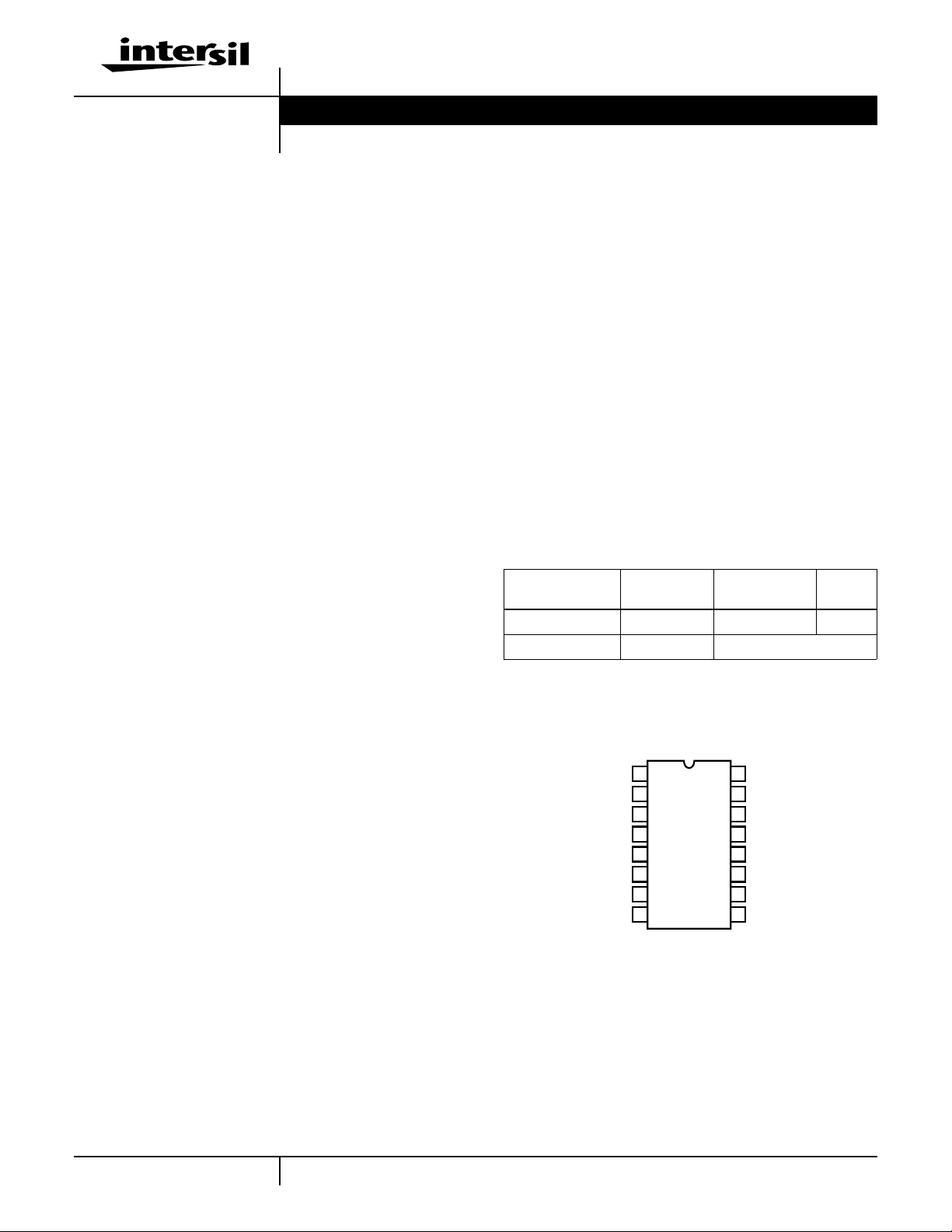
TEMP.RANGE
PART NUMBER
HIP1011ACB 0 to 70 16 Ld SOIC M16.15
HIP1011ACB-T 0 to 70 Tape and Reel
(oC) PACKAGE
PKG.
NO.
Pinout
HIP1011A
(SOIC)
TOP VIEW
User programmability of the overcurrent threshold, fault
reporting response time, latch-off response time and turn-on
slew rate is provided. A resistor connected to the OCSET pin
programs the OC threshold. A capacitor may be added to
the FLTNpin to adjust both the delay time to reporting a fault
and the latch-off of the supplies after an OC or UV event.
Capacitors connected to the gate pins set the turn-on rate. In
addition the HIP1011A has also been enhanced to tolerate
spurious system noise.
1
CAUTION: These devices are sensitive to electrostatic discharge; follow proper IC Handling Procedures.
FLTN
3V5VG
V
CC
12VIN
3VS
1
2
3
4
5
6
7
8
M12VIN
3VISEN
OCSET
1-888-INTERSIL or 321-724-7143
M12VO
16
M12VG
15
12VG
14
GND
13
12VO
12
5VISEN
11
5VS
10
PWRON
9
| Copyright © Intersil Corporation 2000
Page 2
Typical Application
3.3V INPUT
HIP1011A
3.3V,
7.6A OUT 0.5A OUT 0.1A OUT 5A OUT
5mΩ, 1%
12V,
5V,-12V,
5mΩ, 1%
5V INPUT
HUF761315K8
-12V INPUT
12V INPUT
POWER CONTROL INPUT
NOTE: All capacitors are ±10%.
Simplified Schematic
V
CC
V
CC
100µA
OCSET
PWRON
GND
V
CC
5V ZENER
REFERENCE
V
CC
12VIN
POWER-ON
RESET
V
CC
V
V
5VREF
OCSET
CC
SET (LOW = FAULT)
LOW WHEN V
HIP1011A
M12VIN
FLTN
3V5VG
V
CC
12VIN
3VISEN
3VS
6.04kΩ
1%
FAULT OUTPUT (ACTIVE LOW)
< 10V
CC
OCSET
(OPTIONAL)
RESET
HIGH = FAULT
M12VO
M12VG
12VG
GND
12VO
5VISEN
5VS
PWRON
5VREF
COMP
COMP
COMP
HIGH = SWITCHES ON
COMP
0.033µF
0.033µF
FAULT LATCH
+
-
V
OCSET
+
-
-
+
-
+
V
OCSET
V
OCSET
V
OCSET
-
/13.3
-
+
-
+
-
0.033µF
LOW = FAULT
COMP
INHIBIT
COMP
INHIBIT
COMP
/17
INHIBIT
+
+
/0.8
/3.3
+
-
+
-
+
V
V
4.6V
2.9V
10.8V
CC
CC
0.3Ω
0.7Ω
FLTN
5VS
3V5VG
5VISEN
3VS
3VISEN
12VIN
12VG
12VO
M12VIN
M12VG
M12VIN
M12VO
2
Page 3

HIP1011A
Pin Descriptions
PIN NO. DESIGNATOR FUNCTION DESCRIPTION
1 M12VIN -12V Input -12V Supply Input. Also provides power to the -12V overcurrent circuitry.
2 FLTN Fault Output 5V CMOS Fault Output; LOW = FAULT.A capacitor may be placed from this pin to ground to
provide delay time to fault notification and power supply latch-off.
3 3V5VG 3.3V/5V Gate Output Drive the gates of the 3.3V and 5V MOSFETs. Connect a capacitor to ground to set the start-
up ramp. During turn on, this capacitor is charged with a 25µA current source.
4 VCC 12V VCC Input Connect to unswitched 12V supply.
5 12VIN 12V Input Switched 12V supply input.
6 3VISEN 3.3V Current Sense Connect to the load side of the current sense resistor in series with source of external 3.3V
MOSFET.
7 3VS 3.3V Source Connect to source of 3.3V MOSFET. This connection along with pin 6 (3VISEN) senses the
voltage drop across the sense resistor.
8 OCSET Overcurrent Set Connecta resistor from this pin to ground to set the overcurrent trip point of all four switches.
All four over current trips can be programmed by changing the value of this resistor. The
default (6.04kΩ, 1%) is compatible with the maximum allowable currents as outlined in the
PCI specification.
9 PWRON Power On Control Controls all four switches. High to turn switches ON, Low to turn them OFF.
10 5VS 5V Source Connect to source of 5V MOSFET switch. This connection along with pin 11 (5VISEN)
senses the voltage drop across the sense resistor.
11 5VISEN 5V Current Sense Connect to the load side of the current sense resistor in series with source of external 5V
MOSFET.
12 12VO Switched 12V Output Switched 12V output.
13 GND Ground Connect to common of power supplies.
14 12VG Gate of Internal PMOS Connect a capacitor between 12VG and 12VO to set the start up ramp for the +12V supply.
This capacitor is charged with a 25µA current source during start-up. The UV circuitry is
enabled after the voltage on 12VG is less than 400mV.Therefore,if the capacitor on the pin
3 (3V5VG) is more than 25% larger than the capacitor on pin 14 (12VG) a false UV may be
detected during start up.
15 M12VG Gate of Internal NMOS Connect a capacitor between M12VG and M12VO to set the start up ramp for the M12V
supply. This capacitor is charged with 25µA during start up.
16 M12VO Switched -12V
Output
Switched 12V Output.
3
Page 4
HIP1011A
Absolute Maximum Ratings Thermal Information
VCC, 12VIN . . . . . . . . . . . . . . . . . . . . . . . . . . . . . . . -0.5V to +14.0V
12VO . . . . . . . . . . . . . . . . . . . . . . . . . . . . . . . -0.5V to V
12VIN
+0.5V
12VO, 12VG, 3V5VG . . . . . . . . . . . . . . . . . . . . . -0.5V to VCC+0.5V
M12VIN . . . . . . . . . . . . . . . . . . . . . . . . . . . . . . . . . . -15.0V to +0.5V
M12VO, M12VG. . . . . . . . . . . . . . . . . . . . . . V
M12VIN
-0.5V to +0.5V
3VISEN, 5VISEN . . . . . . . . . . . -0.5V to the Lesser of VCC or +7.0V
Voltage, Any Other Pin. . . . . . . . . . . . . . . . . . . . . . . . -0.5V to +7.0V
12VO Output Current. . . . . . . . . . . . . . . . . . . . . . . . . . . . . . . . . . .3A
M12VO Output Current . . . . . . . . . . . . . . . . . . . . . . . . . . . . . . . 0.8A
ESD Classification . . . . . . . . . . . . . . . . . . . . . . . . . . . . .4KeV (HBM)
Operating Conditions
VCC Supply Voltage Range. . . . . . . . . . . . . . . . . .+10.8V to +13.2V
±12V, 5V and 3.3V Input Supply Tolerances . . . . . . . . . . . . . . . .±10%
12VO Output Current. . . . . . . . . . . . . . . . . . . . . . . . . . . . 0 to +0.5A
M12VO Output Current . . . . . . . . . . . . . . . . . . . . . . . . . . 0 to +0.1A
Temperature Range (TA) . . . . . . . . . . . . . . . . . . . . . . . .0oC to 70oC
CAUTION: Stresses above those listed in “Absolute Maximum Ratings” may cause permanent damage to the device. This is a stress only rating and operation of the
device at these or any other conditions above those indicated in the operational sections of this specification is not implied.
NOTES:
1. θJA is measured with the component mounted on a low effective thermal conductivity test board in free air. See Tech Brief 379 for details.
2. All voltages are relative to GND, unless otherwise specified.
Thermal Resistance (Typical, Note 1) θJA (oC/W)
SOIC Package . . . . . . . . . . . . . . . . . . . . . . . . . . . . . 105
Maximum Junction Temperature . . . . . . . . . . . . . . . . . . . . . . .125oC
Maximum Storage Temperature Range. . . . . . . . . . -65oC to 150oC
Maximum Lead Temperature (Soldering 10s) . . . . . . . . . . . . .300oC
(SOIC - Lead Tips Only)
Die Characteristics
Number of Transistors . . . . . . . . . . . . . . . . . . . . . . . . . . . . . . . . .290
Electrical Specifications Nominal 5.0V and 3.3V Input Supply Voltages,
VCC = 12VIN = 12V, M12VIN = -12V, TA = TJ= 0 to 70oC, Unless Otherwise Specified
PARAMETER SYMBOL TEST CONDITIONS MIN TYP MAX UNITS
5V/3.3V SUPPLY CONTROL
5V Overcurrent Threshold I
5V Overcurrent Threshold Voltage V
5V Overcurrent Threshold Voltage V
5V Undervoltage Trip Threshold V
5V Undervoltage Fault Response Time t
5V Turn-On Time
OC5V
OC5V_1
OC5V_2
5VUV
5VUV
t
ON5V
(PWRON High to 5VOUT = 4.75V)
5VS Input Bias Current IB
5VISEN Input Bias Current IB
3V Overcurrent Threshold I
3V Overcurrent Threshold Voltage V
3V Overcurrent Threshold Voltage V
3V Undervoltage Trip Threshold V
3V Undervoltage Fault Response Time t
3V Turn-On Time
5VS
5VISEN
OC3V
OC3V_1
OC3V_2
3VUV
3VUV
t
ON3V
(PWRON High to 3VOUT = 3.00V)
3VS Input Bias Current IB
3VISEN Input Bias Current IB
3VS
3VISEN
3V5VG Vout Low Vout_lo_35VG PWRON = Low, FLTN = Low - 0.1 0.4 V
3V5VG Vout High Vout_hi_35VG PWRON = High, FLTN = High 10.5 11.1 - V
Gate Output Charge Current IC
3V5VG
See Typical Application Diagram - 7.1 - A
V
= 0.6V 30 36 42 mV
OCSET
V
= 1.2V 66 72 79 mV
OCSET
4.42 4.65 4.75 V
- 150 350 ns
C
3V5VG
= 0.022µF, C
5VOUT
= 2000µF,
- 6.5 - ms
RL = 1Ω
PWRON = High -40 -26 -20 µA
PWRON = High -160 -140 -110 µA
See Typical Application Diagram - 9.0 - A
V
= 0.6V 42 49 56 mV
OCSET
V
= 1.2V 88 95 102 mV
OCSET
2.74 2.86 2.97 V
- 150 350 ns
C
3V5VG
= 0.022µF, C
3VOUT
= 2000µF,
- 6.5 - ms
RL = 0.43Ω
PWRON = High -40 -26 -20 µA
PWRON = High -160 -140 -110 µA
PWRON = High, V
= 2V 22.5 25.0 27.5 µA
3V5VG
4
Page 5

HIP1011A
Electrical Specifications Nominal 5.0V and 3.3V Input Supply Voltages,
VCC = 12VIN = 12V, M12VIN = -12V, TA = TJ= 0 to 70oC, Unless Otherwise Specified (Continued)
PARAMETER SYMBOL TEST CONDITIONS MIN TYP MAX UNITS
Gate Turn-On Time
(PWRON High to 3V5VG = 11V)
Gate Turn-Off Time t
Gate Turn-Off Time C
+12V SUPPLY CONTROL
On Resistance of Internal PMOS r
Overcurrent Threshold I
Overcurrent Threshold I
12V Undervoltage Trip Threshold V
Undervoltage Fault Response Time t
Gate Charge Current IC
Turn-On Time
(PWRON High to 12VG = 1V)
Turn-Off Time t
Turn-Off Time C
-12V SUPPLY CONTROL
On Resistance of Internal NMOS r
Overcurrent Threshold I
Overcurrent Threshold I
Gate Output Charge Current IC
Turn-On Time
(PWRON High to M12VG = -1V)
Turn-On Time
(PWRON High to M12VO = -10.8V)
Turn-Off Time t
Turn-Off Time C
M12VIN Input Bias Current IB
CONTROL I/O PINS
Supply Current I
OCSET Current I
Overcurrent to Fault Response Time t
Overcurrent to Fault Response Time FLTN Cap = 1000pF - 2200 - ns
Overcurrent to Fault Response Time FLTN Cap = 10µF - 30 - µs
PWRON Threshold Voltage V
FLTN Output Low Voltage V
FLTN Output High Voltage V
FLTN Output Latch Threshold V
12V Power On Reset Threshold V
t
ON3V5V
OFF3V5V
DS(ON)12
OC12V_1
OC12V_2
12VUV
12VUV
12VG
t
ON12V
OFF12V
DS(ON)M12
OC12V_1
OC12V_2
M12VG
t
ONM12V
t
ONM12V
OFFM12V
M12VIN
VCC
OCSET
OC
THPWRON
FLTN,OLIFLTN
FLTN,OHIFLTN
FLTN,TH
POR,TH
C
= 0.1µF - 280 500 µs
3V5VG
C
= 0.1µF, 3V5VG from 9.5V to 1V - 13 17 µs
3V5VG
=0.022µF,3V5VGFalling90%to
3V5VG
-2-µs
10%
PWRON = High, ID = 0.5A,
0.18 0.3 0.35 Ω
TA = TJ = 25oC
V
= 0.6V 0.6 0.75 0.9 A
OCSET
V
= 1.2V 1.25 1.50 1.8 A
OCSET
10.5 10.8 11.15 V
- 150 - ns
PWRON = High, V
C
= 0.022µF - 16 20 ms
12VG
C
= 0.1µF, 12VG - 9 12 µs
12VG
= 0.022µF, 12VG Rising
12VG
= 3V 23.5 25.0 28.5 µA
12VG
-3-µs
10% - 90%
PWRON = High, ID = 0.1A,
0.5 0.7 0.9 Ω
TA = TJ = 25oC
V
= 0.6V 0.15 0.18 0.25 A
OCSET
V
= 1.2V 0.30 0.37 0.50 A
OCSET
PWRON = High, V
C
= 0.022µF - 160 300 µs
M12VG
C
= 0.022µF, C
M12VG
= -4V 22.5 25 27.5 µA
3VG
M12VO
= 50µF,
-16-ms
RL = 120Ω
C
= 0.1µF, M12VG - 18 23 µs
M12VG
= 0.022µF, M12VG Falling 90%
M12VG
-3-µs
to 10%
PWRON = High - 2 2.6 mA
4 5 5.8 mA
95 100 105 µA
FLTN Cap = 100pF - 500 960 ns
0.8 1.6 2.1 V
= 2mA - 0.6 0.9 V
= 0 to -4mA 3.9 4.3 4.9 V
1.8 2.3 3 V
VCC Voltage Falling 9.4 10 10.6 V
5
Page 6

Typical Performance Curves
HIP1011A
340
320
+12 (mΩ)
300
ON
PMOS r
280
260
0 5 10 15 20 25 30 35 40 45 50 55 60 65 70
NMOS -12 r
ON
PMOS +12 r
TEMPERATURE (oC)
ON
FIGURE 1. rON vs TEMPERATURE FIGURE 2. UV TRIP vs TEMPERATURE
10.84
10.83
1000
900
800
700
600
-12 (mΩ)
ON
NMOS r
4.632
4.631
4.630
4.629
5V UVTRIP (V)
4.628
4.627
4.626
0 5 10 15 20 25 30 35 40 45 50 55 60 65 70
TEMPERATURE (oC)
100
90
80
3V OCVth
5 UV
3.3 UV
2.862
2.861
2.860
3.3V UVTRIP (V)
2.859
2.858
12 UV TRIP (V)
10.82
10.81
0 5 10 15 20 25 30 35 40 45 50 55 60 65 70
TEMPERATURE (oC)
FIGURE 3. 12 UV TRIP vs TEMPERATURE FIGURE 4. OC Vth vs TEMPERATURE (VR
102
101
100
IOC SET (mA)
99
98
0 5 10 15 20 25 30 35 40 45 50 55 60 65 70
OC Vth (mV)
70
60
TEMPERATURE (oC)
5V OCVth
0 5 10 15 20 25 30 35 40 45 50 55 60 65 70
TEMPERATURE (oC)
= 1.21V)
OCSET
FIGURE 5. OCSET I vs TEMPERATURE
6
Page 7

Typical Performance Curves (Continued)
HIP1011A
3V5VG
5V Iout
TIME (1µs /DIV)
FLTN
VOLTAGE (2V / DIV)
CURRENT (5A / DIV)
3V5VG
5V Iout
TIME (1µs /DIV)
FLTN
FLTN
VOLTAGE (2V / DIV)
CURRENT (5A / DIV)
FIGURE 6. FLTN, 3V5VG RESPONSE TO OC, FLTN = 100pF FIGURE 7. FLTN, 3V5VG RESPONSE TO OC, FLTN CAP = 0.001µF
3V5VG
5V Iout
FLTN
3V5VG
5V Iout
FLTN
VOLTAGE (2V / DIV)
CURRENT (5A / DIV)
TIME (2µs /DIV)
VOLTAGE (2V / DIV)
CURRENT (5A / DIV)
TIME (50µs /DIV)
FIGURE 8. FLTN, 3V5VG RESPONSE TO OC, FL TNCAP = 0.01µF FIGURE 9. FLTN, 3V5VG RESPONSE TO OC, FLTN CAP = 1µF
10ms
1ms
VG
100µs
10µs
1µs
100ns
10ns
1ns
100pF
0.001µF 0.1µF1µF10µF
0.01µF
FIGURE 10. RESPONSE TIME vs FLTN CAP
7
Page 8

HIP1011A
HIP1011A PCI Hot Plug Controller
Key Feature Description and Operation
A drop-in alternative to the widely used HIP1011, the
HIP1011A additionally features an adjustable delay time to
fault reporting and latch-off of the MOSFET switches. During
an over current condition (OC) on any output, or an under
voltage (UV) condition on the +5V, +3.3V or +12V outputs, a
LOW (0V) is presented on the FLTN output and all
MOSFETs are latched-off. A programmable delay time from
an OC or UV event to the FLTN signal going LOW and
MOSFET latch-off can be designed into the system by a
single capacitor from the FLTNpin to ground. The addition of
an increasingly larger capacitor value on the FLTN pin
increases the time from the OC or UV occurrence to the start
of the FLTN high to low transition. The capacitor also slows
the falling ramp thus delaying reaching the FLTN latch
threshold of ~2.4V.Once the FLTN latch voltage threshold is
reached the HIP1011A then simultaneously shuts down all
four supplies. This added feature enables the HIP1011A to
ignore both transient UV and OC events to the extent of a
single capacitor value in the system design. This feature also
may allow the system OS to complete housekeeping
activities in preparation for a possible unplanned shutdown
of the affectedcard by receiving an early warning signal from
the HIP1011A.
Customizing and Optimizing Circuit Performance
and Functionality
HOW ADJUSTABLE IS THE FAULT REPORTING DELAY
AND TIME TO POWER SUPPLY LATCH-OFF?
Figure 12 illustrates the relationship between the FLTN
signal and the gate drive outputs. Duration
time between FLTN starting to transition from High to Low,
a, indicates the
(indicating a fault has occurred) and the start of the gate
drive outputs latching off. The latch-off is initiated by the
falling FLTN signal reaching the output latch threshold
voltage, V
FLTN, TH
. Table 1 illustrates the effect of the FLTN
capacitor on the response time.
TABLE 1. RESPONSE TIME TABLE
0.001µF 0.1µF10µF
3V5VG Response a 0.85µs37µs 3.8ms
V
FLTN, TH
FLTN
a
3V5VG
T1 T2
FIGURE 12. TIMING DIAGRAM
CAN THE HIP1011A BE USED ON A CompactPCI
BOARD?
Yes, the HIP1011A can be used on a CompactPCI card
application. See Technical Brief TB358.
NOTE:
3. All capacitors are ±10%.
3.3V INPUT
-12V INPUT
12V INPUT
POWER CONTROL INPUT
5mΩ 1%
6.04kΩ
8
3.3V
7.6A OUT 0.5A OUT 0.1A OUT 5A OUT
1%
FAULT OUTPUT (ACTIVE LOW)
FIGURE 11. HIP1011A TYPICAL APPLICATION
12V
HIP1011A
M12VIN
FLTN
3V5VG
V
12VIN
3VISEN
3VS
OCSET
M12VO
M12VG
CC
5VISEN
PWRON
(SEE TABLE 1)
12VG
GND
12VO
5VS
5V-12V
0.033µF
0.033µF
5mΩ 1%
5V INPUT
0.033µF
Page 9

HIP1011A
ARE THERE PCB LAYOUT DESIGN BEST PRACTICES
TO FOLLOW? WHAT ARE THEY?
As with most innovative ICs performing critical tasks there
are crucial PCB layout best practices to follow for optimal
performance. PCB traces that connect each end of the
current sense resistors to the HIP1011A must not carry any
load current. This can be accomplished by two dedicated
PCB traces directly from the sense resistor to the HIP1011A,
see examples of correct and incorrect layouts in Figure 13.
CORRECT
TO HIP1011A
VS AND VISEN
FIGURE 13. SENSE RESISTOR LAYOUT
INCORRECT
TO HIP1011A
VS AND VISEN
CURRENT
SENSE RESISTOR
Typical Applications: HIP1011A PCI Hot
Plug Controller
inch SOICs. The typical application requires only 1.1 square
inches of PCB board space.
0.75in
1.5in
FIGURE 14. LAYOUT PLOT, ACTUAL SIZE (0.75in x 1.5in)
IS THERE A HIP1011A PCI HOT PLUG EVALUATION
BOARD AVAILABLE?
There is an evaluation board available through your local
Intersil sales office. The HIP1011AEVAL1 board (Figure 15)
is a simple board designed to demonstrate and evaluate the
HIP1011A using an external PWRON signal simulating a
PCI Hot Plug environment. The HIP1011AEVAL1 board
comes in 2 parts, the mother board with the HIP1011A,
MOSFETs with external components and a load board
simulating a ‘typical’ PCI load with adequate space for
modifying the existingload or to add an electronic load. Even
with a number of available test points the HIP1011A
implementation space is still very efficient. In addition, the
demo board offers adequate space to evaluate the
application note discussions found in AN9737.
Introduction to HIP1011A and PCI Hot Plug
Evaluation Board
The HIP1011A is compatible with the PCI Hot Plug
specification as it is derived from the widely used HIP1011.
This device facilitates “HOT PLUGGING”, the removal or
insertion of PCI compliant cards without the need to power
down the server voltage bus. The HIP1011A controls all four,
-12V, +12V, +3.3V, +5V supplies found in PCI applications,
monitoring and protecting all against over current (OC) and
the +12V, +3.3V, +5V for under voltage (UV) conditions.
Reference the PCI Hot Plug specification available from
www.pcisig.com.
Figure 14 illustrates the PCB pattern for implementation of
the HIP1011A with 4 power MOSFETs. Additional
components for optimizing performance in particular
applications, ambient electrical noise levels or desired
features will be necessary. The ease of implementation of
the HIP1011A and MOSFETs is complemented by the small
PCB foot print necessary, since both are available in 0.150
9
Page 10

HIP1011A
M12VIN
FLTN
3V5VG
V
CC
12VIN
3VISEN
3VS
OCSET
R4 C4
D1
5V
BUS BOARD
-12VOUT
HIP1011A
M12VO
M12VG
12VG
GND
12VO
5VISEN
5VS
PWRON
JP2
PWRON IN
3.3V INPUT
-12V INPUT
V
CC
12V INPUT
Q1, Q2
TP2
TP3
TP4
3, 4, 5 TP8 2 TP6 1 TP7 9, 11, 12 TP5 7, 8, 10 TP9
R2
TP1
JP1
R3
FIGURE 15. HIP1011AEVAL1
Table 2 details the BOM for the HIP1011AEVAL1 board.
5VOUT12VOUT3.3VOUT GND
R1
C1
C2
6
TP10
TP11
5V INPUT
Q3, Q4
C3
INDICATES BANANA JACKS
INDICATES EDGE CONNECTOR CARD
INDICATES EDGE CONNECTOR SOCKET
LOAD BOARD
RL1
3.3V
CL1
RL2
5.0V
CL2
RL3
+12V
CL3
RL4
-12V
CL4
TABLE 2.
COMPONENT
DESIGNATOR COMPONENT NAME COMPONENT DESCRIPTION
U1 HIP1011ACB PCI Hot Plug Controller Intersil Corporation, HIP1011ACB PCI Hot Plug Controller
Q1, Q2, Q3, Q4 RF1K49211 Intersil Corporation, RF1K49211 7A, 12V, 20mΩ, Logic Level
N-Channel MOSFET
R1, R2 R
for 3.3V and 5V Supplies Dale, WSL-2512 10mΩ Metal Strip Resistor
SENSE
C1, C2, C3 Gate Timing Capacitors 0.033µF 805 Chip Capacitor
R3 Over Current Set Resistor 12.1kΩ 805 Chip Resistor
C4 Fault Stability Capacitor 100pF 805 Chip Cap
Conn. 1 Connector for Load Card Sullins EZM06DRXH
R4 LED Series Resistor 4.7kΩ 805 Chip Resistor
D1 Fault Indicating LED Red LED
JP1 VCC to Switched or Unswitched 12V Supply 0.01” Spaced Pins for Jumper Block
JP2 PWRON to 5V 0.01” Spaced Pins for Jumper Block
RL1 3.3V Load Board Resistor 1.1Ω, 10W
RL2 5.0V Load Board Resistor 2.5Ω, 10W
RL3 +12V Load Board Resistor 47Ω, 5W
RL4 -12V Load Board Resistor 240Ω, 2W
CL1, CL2 +3.3V and +5.0V Load Board Capacitor 2200µF
CL3, CL4 +12V and -12V Load Board Capacitor 100µF
10
Page 11

Small Outline Plastic Packages (SOIC)
HIP1011A
N
INDEX
AREA
123
-A-
E
-B-
SEATING PLANE
D
A
-C-
0.25(0.010) BM M
H
L
h x 45
o
α
e
B
0.25(0.010) C AM BS
M
NOTES:
1. Symbols are defined in the “MO Series Symbol List” in Section 2.2 of
Publication Number 95.
2. Dimensioning and tolerancing per ANSI Y14.5M-1982.
3. Dimension “D” does not include mold flash, protrusions or gate burrs.
Mold flash, protrusion and gate burrs shall not exceed 0.15mm (0.006
inch) per side.
4. Dimension“E” does notincludeinterlead flash orprotrusions.Interlead
flash and protrusions shall not exceed 0.25mm (0.010 inch) per side.
5. The chamfer on the body is optional. If it is not present, a visual index
feature must be located within the crosshatched area.
6. “L” is the length of terminal for soldering to a substrate.
7. “N” is the number of terminal positions.
8. Terminal numbers are shown for reference only.
9. Thelead width“B”,as measured0.36mm(0.014 inch)orgreater above
the seating plane, shall not exceed a maximum value of 0.61mm
(0.024 inch).
10. Controlling dimension: MILLIMETER. Converted inch dimensions are
not necessarily exact.
A1
C
0.10(0.004)
M16.15 (JEDEC MS-012-AC ISSUE C)
16 LEAD NARROW BODY SMALL OUTLINE PLASTIC
PACKAGE
INCHES MILLIMETERS
SYMBOL
A 0.0532 0.0688 1.35 1.75 -
A1 0.0040 0.0098 0.10 0.25 -
B 0.013 0.020 0.33 0.51 9
C 0.0075 0.0098 0.19 0.25 D 0.3859 0.3937 9.80 10.00 3
E 0.1497 0.1574 3.80 4.00 4
e 0.050 BSC 1.27 BSC H 0.2284 0.2440 5.80 6.20 -
h 0.0099 0.0196 0.25 0.50 5
L 0.016 0.050 0.40 1.27 6
N16 167
o
α
0
o
8
o
0
o
8
Rev. 0 12/93
NOTESMIN MAX MIN MAX
-
All Intersil semiconductor products are manufactured, assembled and tested under ISO9000 quality systems certification.
Intersil semiconductor products are sold by description only. Intersil Corporation reserves the right to make changes in circuit design and/or specifications at any time without notice. Accordingly , the reader is cautioned to verify that data sheets are current before placing orders. Information furnished by Intersil is believed to be accurate and
reliable. However, no responsibility is assumed by Intersil or its subsidiaries for its use; nor for any infringements of patents or other rights of third parties which may result
from its use. No license is granted by implication or otherwise under any patent or patent rights of Intersil or its subsidiaries.
For information regarding Intersil Corporation and its products, see web site www.intersil.com
Sales Office Headquarters
NORTH AMERICA
Intersil Corporation
P. O. Box 883, Mail Stop 53-204
Melbourne, FL 32902
TEL: (321) 724-7000
FAX: (321) 724-7240
11
EUROPE
Intersil SA
Mercure Center
100, Rue de la Fusee
1130 Brussels, Belgium
TEL: (32) 2.724.2111
FAX: (32) 2.724.22.05
ASIA
Intersil (Taiwan) Ltd.
7F-6, No. 101 Fu Hsing North Road
Taipei, Taiwan
Republic of China
TEL: (886) 2 2716 9310
FAX: (886) 2 2715 3029
 Loading...