

Datasheet HIN241IA, HIN241, HIN238, HIN237IP, HIN237IB Datasheet (Intersil Corporation)
...Page 1
TM
HIN230 thru HIN241
Data Sheet May 2000
+5V Powered RS-232
Transmitters/Receivers
The HIN230-HIN241 family of RS-232 transmitters/receivers
interfacecircuits meet all ElA RS-232E and V.28specifications,
and are particularly suited forthose applications where ±12V is
not available . The y require a single +5V po wer supply (except
HIN231 and HIN239) and feature onboard charge pump
voltage converters which generate +10V and -10V supplies
from the 5V supply. The HIN233 and HIN235 require no
externalcapacitors and are ideally suited for applications where
circuit board space is critical. The family of devices offer a wide
variety of RS-232 transmitter/receiver combinations to
accommodate various applications (see Selection Table).
The drivers feature true TTL/CMOS input compatibility, slewrate-limited output, and 300Ω power-off source impedance.
The receivers can handle up to ±30V, and have a 3kΩ to 7kΩ
input impedance. The receivers also feature hysteresis to
greatly improve noise rejection.
File Number 3138.7
Features
• Meets All RS-232E and V.28 Specifications
• Requires Only Single +5V Power Supply
- (+5V and +12V - HIN231 and HIN239)
• High Data Rate. . . . . . . . . . . . . . . . . . . . . . . . . . .120kbps
• HIN233 and HIN235 Require No External Capacitors
• Onboard Voltage Doubler/Inverter
• Low Power Consumption
• Low Power Shutdown Function
• Three-State TTL/CMOS Receiver Outputs
• Multiple Drivers
- ±10V Output Swing for 5V lnput
- 300Ω Power-Off Source Impedance
- Output Current Limiting
- TTL/CMOS Compatible
- 30V/µs Maximum Slew Rate
• Multiple Receivers
- ±30V Input Voltage Range
-3kΩ to 7kΩ Input Impedance
- 0.5V Hysteresis to Improve Noise Rejection
Applications
• Any System Requiring RS-232 Communication Ports
- Computer - Portable, Mainframe, Laptop
- Peripheral - Printers and Terminals
- Instrumentation
- Modems
Selection Table
NUMBER OF
PART
NUMBER
HIN230 +5V 5 0 4 Capacitors Yes/No 20
HIN231 +5V and +7.5V to 13.2V 2 2 2 Capacitors No/No 16
HIN232 +5V 2 2 4 Capacitors No/No 16
HIN233 +5V 2 2 None No/No 20
HIN234 +5V 4 0 4 Capacitors No/No 16
HIN235 +5V 5 5 None Yes/Yes 24
HIN236 +5V 4 3 4 Capacitors Yes/Yes 24
HIN237 +5V 5 3 4 Capacitors No/No 24
HIN238 +5V 4 4 4 Capacitors No/No 24
HIN239 +5V and +7.5V to 13.2V 3 5 2 Capacitors No/Yes 24
HIN240 +5V 5 5 4 Capacitors Yes/Yes 44
HIN241 +5V 4 5 4 Capacitors Yes/Yes 28
POWER SUPPLY
VOLTAGE
RS-232
DRIVERS
NUMBER OF
RS-232
RECEIVERS
EXTERNAL
COMPONENTS
LOW POWER
SHUTDOWN/TTL
THREE-ST ATE
NUMBER OF
LEADS
3-1
1-888-INTERSIL or 321-724-7143 | Intersil and Design is a trademark of Intersil Corporation. | Copyright © Intersil Corporation 2000
CAUTION: These devices are sensitive to electrostatic discharge; follow proper IC Handling Procedures.
Page 2
Ordering Information
HIN230 thru HIN241
PART
NUMBER
HIN230CB 0 to 70 20 Ld SOIC M20.3
HIN230IB -40 to 85 20 Ld SOIC M20.3
HIN231CB 0 to 70 16 Ld SOIC M16.3
HIN231CP 0 to 70 14 Ld PDIP E14.3
HIN231IB -40 to 85 16 Ld SOIC M16.3
HIN231IP -40 to 85 14 Ld PDIP E14.3
HIN232CP 0 to 70 16 Ld PDIP E16.3
HIN232CB 0 to 70 16 Ld SOIC M16.3
HIN232IP -40 to 85 16 Ld PDIP E16.3
HIN232IB -40 to 85 16 Ld SOIC M16.3
HIN233CP 0 to 70 20 Ld PDIP E20.3
HIN234CB 0 to 70 16 Ld SOIC M16.3
HIN234IB -40 to 85 16 Ld SOIC M16.3
HIN235CP 0 to 70 24 Ld PDIP E24.6
HIN236CP 0 to 70 24 Ld PDIP E24.3
HIN236CB 0 to 70 24 Ld SOIC M24.3
HIN236IP -40 to 85 24 Ld PDIP E24.3
HIN236IB -40 to 85 24 Ld SOIC M24.3
TEMP.
RANGE (oC) PACKAGE PKG. NO.
PART
NUMBER
HIN237CP 0 to 70 24 Ld PDIP E24.3
HIN237CB 0 to 70 24 Ld SOIC M24.3
HIN237IP -40 to 85 24 Ld PDIP E24.3
HIN237IB -40 to 85 24 Ld SOIC M24.3
HIN238CP 0 to 70 24 Ld PDIP E24.3
HIN238CB 0 to 70 24 Ld SOIC M24.3
HIN238IP -40 to 85 24 Ld PDIP E24.3
HIN238IB -40 to 85 24 Ld SOIC M24.3
HIN239CB 0 to 70 24 Ld SOIC M24.3
HIN239CP 0 to 70 24 Ld PDIP E24.3
HIN239IB -40 to 85 24 Ld SOIC M24.3
HIN240CN 0 to 70 44 Ld MQFP Q44.10X10
HIN240IN -40 to 85 44 Ld MQFP Q44.10X10
HIN241CB 0 to 70 28 Ld SOIC M28.3
HIN241IB -40 to 85 28 Ld SOIC M28.3
HIN241CA 0 to 70 28 Ld SSOP M28.209
HIN241IA -40 to 85 28 Ld SSOP M28.209
NOTE: Manyof the surface mountdevicesare availableon tape and
reel; add -T to suffix.
TEMP.
RANGE (oC) PACKAGE PKG. NO.
Pin Descriptions
PIN FUNCTION
V
CC
V+ Internally generated positive supply (+10V nominal), HIN231 and HIN239 require +7.5V to +13.2V.
V- Internally generated negative supply (-10V nominal).
GND Ground lead. Connect to 0V.
C1+ External capacitor (+ terminal) is connected to this lead.
C1- External capacitor (- terminal) is connected to this lead.
C2+ External capacitor (+ terminal) is connected to this lead.
C2- External capacitor (- terminal) is connected to this lead.
T
IN
T
OUT
R
IN
R
OUT
EN Enable input. This is an active low input which enables the receiver outputs. With EN = 5V,the outputs are placed in a high
SHUTDOWN Shutdown Input. With SHUTDOWN = 5V, the charge pump is disabled, the receiver outputs are in a high impedance state
NC No Connect. No connections are made to these leads.
Power Supply Input 5V±10%.
Transmitter Inputs. These leads accept TTL/CMOS levels. An internal 400kΩ pull-up resistor to VCCis connected to each lead.
Transmitter Outputs. These are RS-232 levels (nominally ±10V).
ReceiverInputs. These inputs acceptRS-232 input levels.An internal 5kΩpull-down resistor to GNDis connected to each input.
Receiver Outputs. These are TTL/CMOS levels.
impedance state.
and the transmitters are shut off.
3-2
Page 3
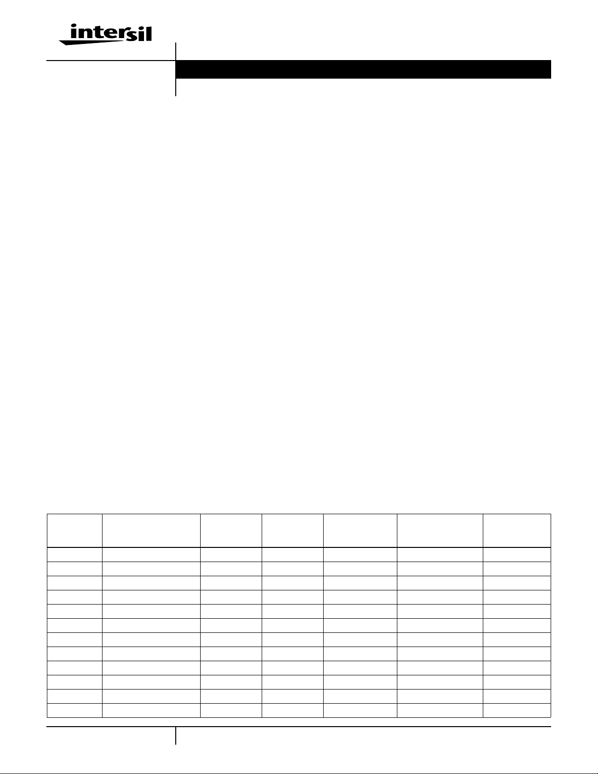
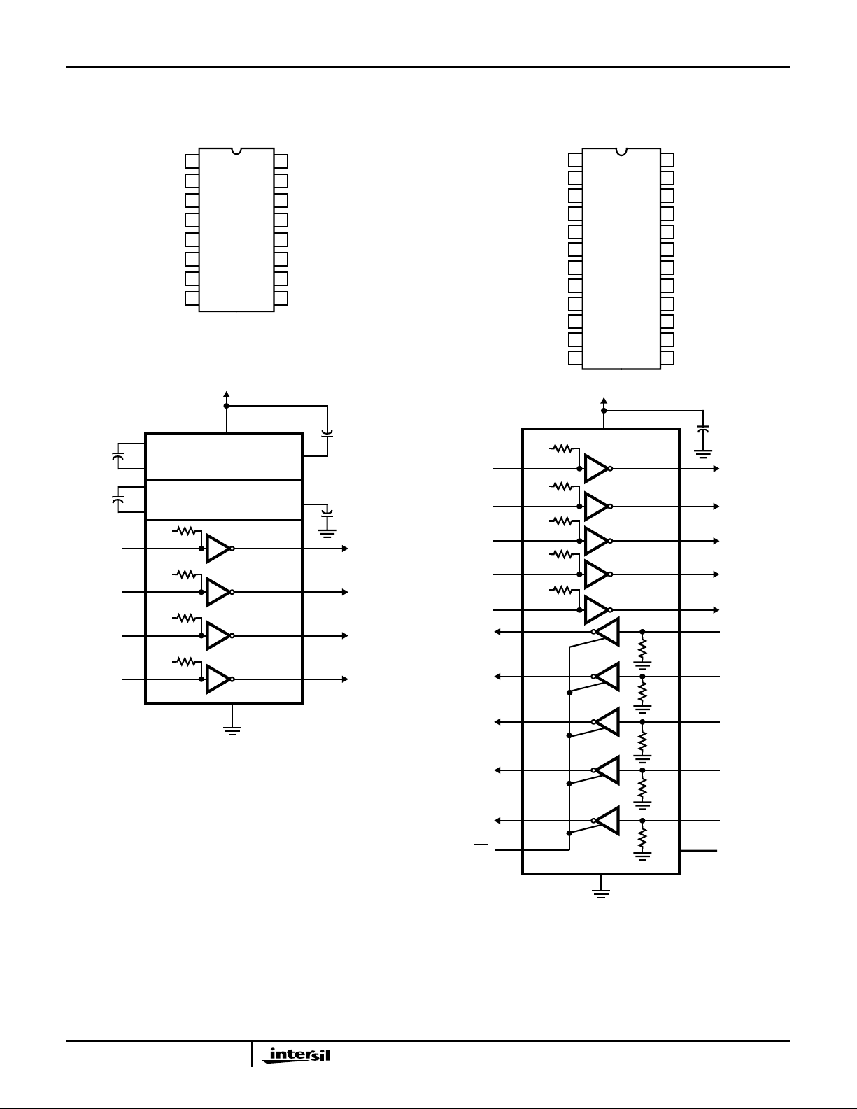
Pinouts
HIN230 (SOIC)
TOP VIEW
HIN230 thru HIN241
HIN231 (SOIC)
TOP VIEW
1
T3
OUT
2
T1
OUT
3
T2
OUT
4
T2
IN
5
T1
IN
6
GND
7
V
CC
8
C1+
9
V+
10
C1-
+5V
8
C1+
+
1µF
10
C1-
11
C2+
+
1µF
12
C2-
+5V
400kΩ
T1
T2
T3
T4
T5
5
IN
+5V
400kΩ
4
IN
+5V
400kΩ
14 1
IN
+5V
400kΩ
15 20
IN
+5V
IN
400kΩ
V
CC
+5V TO 10V
VOLTAGE DOUBLER
+10V TO -10V
VOLTAGE INVERTER
T1
T2
T3
T4
T5
20
T4
OUT
19
T5
IN
18
NC
17
SHUTDOWN
16
T5
OUT
15
T4
IN
14
T3
IN
13
V-
12
C2-
11
C2+
R2
T2
OUT
R2
OUT
T2
C+
NC
1
2
C-
3
V-
4
5
IN
6
7
IN
8
16
V+
(14)
V
CC
GND
T1
R1
R1
T1
NC
OUT
IN
OUT
IN
(13)
(12)
(11)
(10)
(9)
(8)
15
14
13
12
11
10
9
NOTE: Pin numbers in parentheses are for PDIP Package.
+5V
7
V+
V-
1µF
+
9
1
C+
+
13
1µF
1µF
+
2
3
T1
T2
T3
T4
OUT
OUT
OUT
OUT
R1
R2
T1
T2
OUT
OUT
2
10
IN
7
IN
VOLTAGE INVERTER
C-
+5V
400kΩ
+5V
400kΩ
15
V
CC
+12V TO -12V
T1
T2
R1
R2
1619
17
T5
OUT
SHUTDOWN
14
6
+7.5V TO +13.2V
V+
V-
5kΩ
5kΩ
16
3
1µF
+
13
4
1211
56
T1
T2
R1
R2
OUT
OUT
IN
IN
NOTE: SOIC pin numbers shown.
3-3
Page 4
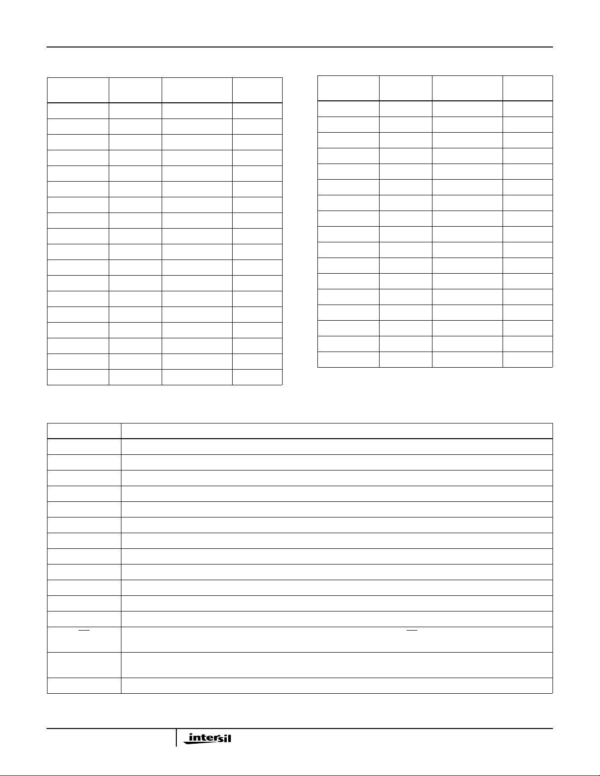
Pinouts (Continued)
HIN232 (PDIP, SOIC)
TOP VIEW
HIN230 thru HIN241
HIN233 (PDIP, SOIC)
TOP VIEW
R1
R2
1µF
1µF
T1
T2
OUT
OUT
T2
C1+
C2+
OUT
R2
V+
C1-
C2-
V-
1
1
2
3
4
5
6
7
8
IN
16
V
CC
15
GND
14
T1
OUT
13
R1
IN
12
R1
OUT
11
T1
IN
10
T2
IN
9
R2
OUT
T2
T1
R1
OUT
R1
T1
OUT
GND
V
CC
(V+) C1+
GND
(V-) C2-
IN
2
IN
3
4
IN
5
6
7
8
9
10
20
19
18
17
16
15
14
13
12
11
R2
OUT
R2
IN
T2
OUT
VC2C2+
V+ (C1-)
C1- (C1+)
V- (C2+)
C2+ (C2-)
NOTE: Pin names in parentheses are for SOIC Package.
+5V
+
1µF
1
C1+
+
3
4
+
5
11
IN
10
IN
VOLTAGE DOUBLER
C1C2+
VOLTAGE INVERTER
C2-
+5V
400kΩ
+5V
400kΩ
16
V
CC
+5V TO 10V
+10V TO -10V
T1
T2
R1
R2
5kΩ
5kΩ
V+
1µF
+
2
T1
IN
+5V
2
400kΩ
+5V
IN
20
8 (13)
13 (14)
12 (10)
17
14 (8)
1
3
C1+
C1VVV+
6
V-
1µF
+
14
7
1312
89
T1
T2
R1
R2
OUT
OUT
IN
IN
T2
R1
OUT
R2
OUT
NO
CONNECT
INTERNAL
-10V
SUPPLY
INTERNAL
+10V
SUPPLY
400kΩ
GND
6
R1
R2
+5V
V
CC
+
6
T1
T2
0.1µF
5
18
4
T1
T2
R1
OUT
OUT
IN
5kΩ
5kΩ
C2+
C2+
C2-
C2-
19
11 (12)
15
16
10 (11)
R2
IN
GND
9
3-4
15
NOTE: Pin numbers in parentheses are for SOIC Package.
Page 5
Pinouts (Continued)
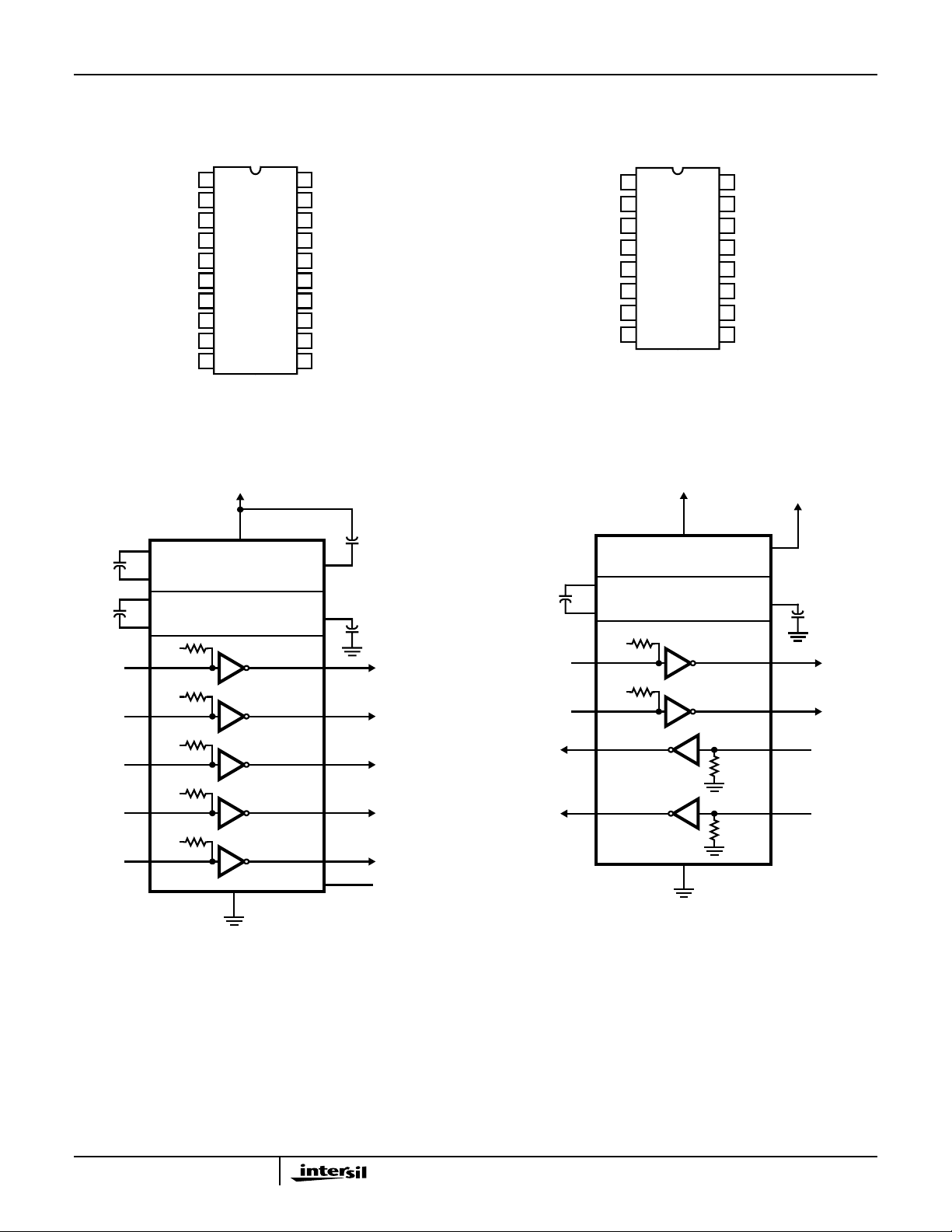
HIN234 (SOIC)
TOP VIEW
HIN230 thru HIN241
HIN235 (PDIP)
TOP VIEW
1
T1
OUT
2
T2
OUT
3
T2
IN
4
T1
IN
5
GND
6
V
CC
7
C1+
8
V+
+5V
7
C1+
+
1µF
1µF
T1
T2
T3
T4
9
C1-
10
C2+
+
11
4
IN
3
IN
13 16
IN
14 15
IN
VOLTAGE INVERTER
C2+5V
400kΩ
+5V
400kΩ
+5V
400kΩ
+5V
400kΩ
V
CC
+5V TO 10V
VOLTAGE DOUBLER
+10V TO -10V
T1
T2
T3
T4
T4
T3
T1
T2
R2
R1
OUT
OUT
OUT
OUT
R2
OUT
T2
T1
OUT
R1
GND
V
CC
1
2
3
4
5
IN
6
7
IN
8
IN
9
10
IN
11
12
16
T3
OUT
15
T4
OUT
14
T4
IN
13
T3
IN
12
V-
11
C2-
10
C2+
9
C1-
24
R3
23
R3
22
T5
IN
21
SHUTDOWN
20
EN
19
T5
OUT
18
R4
17
R4
16
T4
IN
15
T3
IN
14
R5
13
R5
IN
OUT
IN
OUT
OUT
IN
+5V
6
V+
V-
5
1µF
+
8
T1
IN
12
1µF
+
1
2
T1
T2
T3
T4
OUT
OUT
OUT
OUT
R1
R2
R3
R4
R5
T2
T3
T4
T5
OUT
OUT
OUT
OUT
OUT
IN
IN
IN
IN
EN
+5V
400kΩ
8
+5V
7
400kΩ
+5V
15
400kΩ
+5V
16
400kΩ
+5V
400kΩ
22
9
6
23
17
14
20
V
T1
T2
T3
T4
T5
R1
R2
R3
R4
R5
GND
CC
12
5kΩ
5kΩ
5kΩ
0.1µF
+
3
4
2
1
19
10
5
24
18
T1
T2
T3
T4
T5
R1
R2
R3
R4
OUT
OUT
OUT
OUT
OUT
IN
IN
IN
IN
5kΩ
5kΩ
13
21
R5
IN
SHUTDOWN
11
3-5
Page 6

Pinouts (Continued)
HIN236 (PDIP, SOIC)
TOP VIEW
HIN230 thru HIN241
HIN237 (PDIP, SOIC)
TOP VIEW
R1
R2
R3
1
T3
OUT
2
T1
OUT
3
T2
OUT
4
R1
IN
5
R1
OUT
6
T2
IN
7
T1
IN
8
GND
9
V
CC
10
C1+
11
V+
12
C1-
+5V
10
C1+
+
1µF
12
C1-
13
C2+
+
1µF
14
C2-
+5V
400kΩ
T1
T2
T3
T4
OUT
7
IN
+5V
400kΩ
6
IN
+5V
400kΩ
18 1
IN
+5V
400kΩ
19 24
IN
V
CC
+5V TO 10V
VOLTAGE DOUBLER
+10V TO -10V
VOLTAGE INVERTER
T1
T2
T3
T4
R1
OUT
R2
OUT
EN
20
R3
24
T4
23
R2
22
R2
21
SHUTDOWN
20
EN
19
T4
18
T3
17
R3
16
R3
15
V-
14
C2-
13
C2+
OUT
IN
OUT
IN
IN
OUT
IN
T3
T1
T2
R1
OUT
OUT
OUT
R1
OUT
T2
T1
GND
V
CC
C1+
V+
C1-
24
1
2
3
4
IN
5
6
IN
7
IN
8
9
10
11
12
T4
OUT
R2
23
IN
R2
22
OUT
T5
21
IN
T5
20
OUT
T4
19
IN
T3
18
IN
R3
17
OUT
R3
16
IN
V-
15
14
C2C2+
13
+5V
9
V+
V-
1µF
+
11
15
1µF
+
2
3
T1
OUT
T2
OUT
T3
OUT
T4
R1
OUT
IN
45
T1
T2
T3
T4
T5
5kΩ
2322
R2
IN
R1
10
C1+
+
1µF
12
C1-
13
+
1µF
14
7
IN
6
IN
18 1
IN
19 24
IN
21 20
IN
OUT
VOLTAGE DOUBLER
C2+
VOLTAGE INVERTER
C2-
+5V
400kΩ
+5V
400kΩ
+5V
400kΩ
+5V
400kΩ
+5V
400kΩ
5kΩ
R2
R3
OUT
OUT
5kΩ
1617
21
SHUTDOWN
R3
IN
8
9
V
CC
+5V TO 10V
+10V TO -10V
T1
T2
T3
T4
T5
R1
R2
R3
5kΩ
5kΩ
5kΩ
V+
V-
1µF
+
11
15
1µF
+
2
3
45
2322
1617
T1
T2
T3
T4
T5
R1
R2
R3
OUT
OUT
OUT
OUT
OUT
IN
IN
IN
3-6
8
Page 7

Pinouts (Continued)
HIN238 (PDIP, SOIC)
TOP VIEW
HIN230 thru HIN241
HIN239 (SOIC)
TOP VIEW
R1
R2
R3
R4
1µF
1µF
T1
T2
T3
T4
OUT
OUT
OUT
OUT
T2
1
OUT
T1
2
OUT
R2
3
IN
R2
4
OUT
T1
5
IN
R1
6
OUT
R1
7
IN
GND
8
V
9
CC
C1+
10
V+
11
C1-
12
+5V
10
C1+
+
12
C1-
13
+
14
5
IN
18
IN
19 24
IN
21 20
IN
VOLTAGE DOUBLER
C2+
VOLTAGE INVERTER
C2-
+5V
400kΩ
+5V
400kΩ
+5V
400kΩ
+5V
400kΩ
9
V
CC
+5V TO 10V
+10V TO -10V
T1
T2
T3
T4
R1
R2
R3
R4
5kΩ
5kΩ
5kΩ
5kΩ
T3
24
OUT
R3
23
IN
R3
22
OUT
T4
21
IN
T4
20
OUT
T3
19
IN
T2
18
IN
R4
17
OUT
R4
16
IN
V-
15
C2-
14
C2+
13
R1
R5
R4
OUT
R1
GND
V
CC
V+
C1+
C1-
R5
OUT
OUT
R4
T1
1
2
IN
3
4
5
6
7
8
V-
9
IN
10
11
12
IN
24
T2
23
R2
22
R2
21
T2
20
T1
19
R3
18
R3
17
T3
16
15
NC (NOTE)
14
EN
T3
13
IN
IN
OUT
IN
OUT
OUT
IN
OUT
IN
OUT
NOTE: No Connect
+7.5V TO +13.2V
V+
V-
5kΩ
5kΩ
5kΩ
5kΩ
5kΩ
5
8
1µF
+
19
20
2
2122
1817
1211
910
T1
T2
T3
R1
R2
R3
R4
R5
OUT
OUT
OUT
IN
IN
IN
IN
IN
V+
V-
+5V
1µF
+
11
1µF
15
1µF
+
2
1
T1
T2
T3
OUT
OUT
OUT
R1
T1
T2
T3
OUT
6
C1+
+
7
C1-
VOLTAGE INVERTER
+5V
400kΩ
24
IN
+5V
400kΩ
23
IN
+5V
400kΩ
16 13
IN
1
4
V
CC
+10V TO -10V
T1
T2
T3
R1
T4
OUT
76
34
2322
1617
R1
R2
R3
R4
IN
IN
IN
IN
R2
R3
R4
R5
OUT
OUT
OUT
OUT
EN
R2
R3
R4
14
R5
3-7
8
3
Page 8

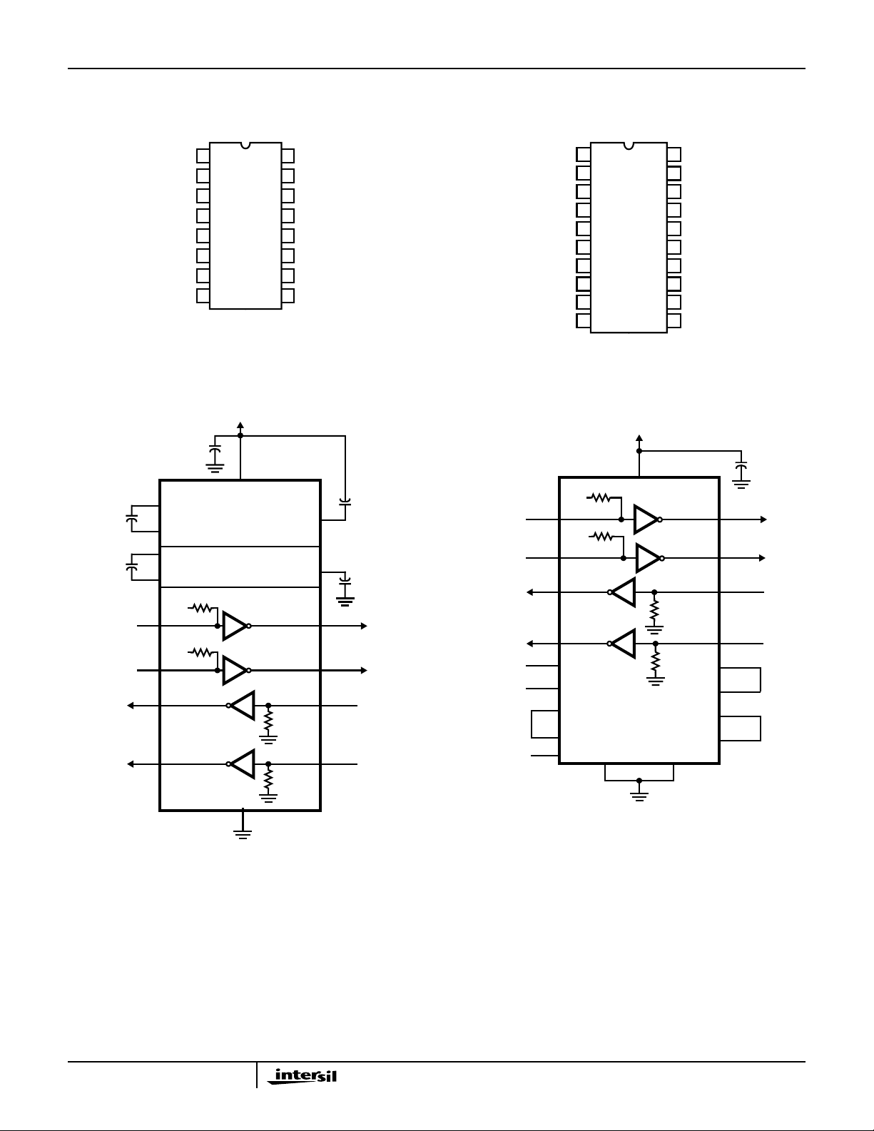
Pinouts (Continued)
NC
SHUT
DOWN
44 43 42 41 40
1
2
3
4
5
6
7
8
9
10
11
12 13 14 15 16 17
NC
OUT
R2
25
C1+
+
27
C1-
28
C2+
+
29
C2-
+5V
400kΩ
15
+5V
400kΩ
14
+5V
400kΩ
37 6
+5V
400kΩ
38 5
+5V
400kΩ
241
16
42
R3
T4
T3
T1
T2
T5
R3
R2
NC
OUT
OUT
OUT
OUT
OUT
NC
NC
R1
R2
R3
R4
R5
IN
IN
IN
1µF
1µF
T1
T2
T3
T4
T5
OUT
OUT
OUT
OUT
OUT
IN
IN
IN
IN
IN
EN
HIN240 (MQFP)
OUT
IN
OUT
T5
R4
T4INT3INR5
R4
EN
39 38 37 36 35 34
IN
IN
OUT
T2INT1
VOLTAGE DOUBLER
VOLTAGE INVERTER
R1
R1
+5V
19
V
CC
+5V TO 10V
+10V TO -10V
T1
T2
T3
T4
T5
R1
R2
R3
R4
R5
18
GND
5kΩ
5kΩ
5kΩ
5kΩ
5kΩ
CC
NCNCNC
V
OUTR5IN
V+
V-
HIN230 thru HIN241
NC
+
1µF
1µF
T1
T2
T3
T4
T5
R1
R2
R3
R4
R5
NC
NC
NC
VC2C2+
C1V+
C1+
NC
NC
OUT
OUT
OUT
OUT
OUT
IN
IN
IN
IN
IN
33
32
31
30
29
28
27
26
25
24
23
2221201918
26
30
7
8
17
1013
43
4039
3536
43
SHUTDOWN
R1
R2
R3
R4
R5
HIN241 (SOIC, SSOP)
TOP VIEW
T3
1
OUT
T1
2
OUT
3
T2
OUT
R2
4
IN
R2
5
OUT
T2
6
IN
T1
7
IN
R1
8
OUT
R1
9
IN
GND
10
V
11
CC
C1+
12
13
V+
14
C1-
+5V
12
C1+
+
1µF
14
C1-
15
C2+
+
1µF
16
C2-
+5V
400kΩ
T1
T2
T3
T4
OUT
OUT
OUT
OUT
OUT
7
IN
+5V
400kΩ
6
IN
+5V
400kΩ
20 1
IN
+5V
400kΩ
21 28
IN
8
24
EN
V
+5V TO 10V
VOLTAGE DOUBLER
+10V TO -10V
VOLTAGE INVERTER
T1
T2
T3
T4
R1
R2
R3
R4
R5
CC
28
T4
OUT
R3
27
IN
R3
26
OUT
SHUTDOWN
25
EN
24
23
R4
IN
R4
22
OUT
T4
21
IN
20
T3
IN
R5
19
OUT
R5
18
IN
V-
17
16
C2C2+
15
11
V+
V-
1µF
+
13
17
1µF
+
2
3
9
T1
T2
T3
T4
R1
OUT
OUT
OUT
OUT
IN
5kΩ
45
R2
IN
5kΩ
2726
R3
IN
5kΩ
2322
R4
IN
5kΩ
5kΩ
1819
25
R5
IN
SHUTDOWN
10
3-8
Page 9

HIN230 thru HIN241
Absolute Maximum Ratings Thermal Information
VCC to Ground. . . . . . . . . . . . . . . . . . . . . .(GND -0.3V) < VCC < 6V
V+ to Ground . . . . . . . . . . . . . . . . . . . . . . . .(VCC -0.3V) < V+ < 12V
V- to Ground. . . . . . . . . . . . . . . . . . . . . . . .-12V < V- < (GND +0.3V)
Input Voltages
TIN . . . . . . . . . . . . . . . . . . . . . . . . . (V- -0.3V) < VIN < (V+ +0.3V)
RIN. . . . . . . . . . . . . . . . . . . . . . . . . . . . . . . . . . . . . . . . . . . . ±30V
Output Voltages
T
. . . . . . . . . . . . . . . . . . . .(V- -0.3V) < V
OUT
R
. . . . . . . . . . . . . . . . . (GND -0.3V) < V
OUT
TXOUT
RXOUT
< (V+ +0.3V)
< (V+ +0.3V)
Short Circuit Duration
T
. . . . . . . . . . . . . . . . . . . . . . . . . . . . . . . . . . . . . .Continuous
OUT
R
. . . . . . . . . . . . . . . . . . . . . . . . . . . . . . . . . . . . . .Continuous
OUT
Operating Conditions
Temperature Range
HIN2XXCX . . . . . . . . . . . . . . . . . . . . . . . . . . . . . . . . .0oC to 70oC
HIN2XXIX. . . . . . . . . . . . . . . . . . . . . . . . . . . . . . . . -40oC to 85oC
CAUTION: Stresses above those listed in “Absolute Maximum Ratings” may cause permanent damage to the device. This is a stress only rating and operation of the
device at these or any other conditions above those indicated in the operational sections of this specification is not implied.
NOTE:
1. θJA is measured with the component mounted on an evaluation PC board in free air.
Thermal Resistance (Typical, Note 1) θJA (oC/W)
14 Ld PDIP Package . . . . . . . . . . . . . . . . . . . . . . . . 90
16 Ld PDIP Package . . . . . . . . . . . . . . . . . . . . . . . . 90
20 Ld PDIP Package . . . . . . . . . . . . . . . . . . . . . . . . 80
24 Ld PDIP Package . . . . . . . . . . . . . . . . . . . . . . . . 70
16 Ld SOIC (W) Package. . . . . . . . . . . . . . . . . . . . . 100
20 Ld SOIC Package . . . . . . . . . . . . . . . . . . . . . . . . 120
24 Ld SOIC Package . . . . . . . . . . . . . . . . . . . . . . . . 75
28 Ld SOIC Package . . . . . . . . . . . . . . . . . . . . . . . . 70
28 Ld SSOP Package . . . . . . . . . . . . . . . . . . . . . . . 95
44 Ld MQFP Package . . . . . . . . . . . . . . . . . . . . . . . 80
Maximum Junction Temperature (Plastic Package) . . . . . . . .150oC
Maximum Storage Temperature Range. . . . . . . . . . -65oC to 150oC
Maximum Lead Temperature (Soldering 10s) . . . . . . . . . . . . .300oC
(SOIC, SSOP, MQFP - Lead Tips Only)
Electrical Specifications Test Conditions: V
= +5V ±10%, TA = Operating Temperature Range
CC
PARAMETER TEST CONDITIONS MIN TYP MAX UNITS
SUPPLY CURRENTS
Power Supply Current, I
CC
No Load,
TA = 25oC
HIN232-233 - 5 10 mA
HIN230, HIN234-238, HIN240-241 - 7 15 mA
HIN231, HIN239 - 0.4 1 mA
V+ Power Supply Current, I
No Load, TA = 25oC
CC
No Load,
TA = 25oC
HIN231 - 1.8 5 mA
HIN239 - 5.0 15 mA
Shutdown Supply Current, ICC(SD) TA = 25oC-110µA
LOGIC AND TRANSMITTER INPUTS, RECEIVER OUTPUTS
Input Logic Low, V
Input Logic High, V
lL
lH
TIN, EN, Shutdown - - 0.8 V
T
IN
2.0 - - V
EN, Shutdown 2.4 - - V
Transmitter Input Pullup Current, I
P
TTL/CMOS Receiver Output Voltage Low,V
TTL/CMOS Receiver Output Voltage High, V
OL
OH
TIN = 0V - 15 200 µA
I
= 1.6mA
OUT
(HIN231-HIN233 I
I
= -1.0mA 3.5 4.6 - V
OUT
OUT
= 3.2mA)
- 0.1 0.4 V
RECEIVER INPUTS
RS-232 Input Voltage Range V
Receiver Input Impedance R
IN
IN
VIN = ±3V 3.0 5.0 7.0 kΩ
-30 - +30 V
Receiver Input Low Threshold, VlN (H-L) VCC = 5V, TA = 25oC 0.8 1.2 - V
Receiver Input High Threshold, VIN (L-H) VCC = 5V, TA = 25oC - 1.7 2.4 V
Receiver Input Hysteresis V
HYST
0.2 0.5 1.0 V
TIMING CHARACTERISTICS
Baud Rate (1 Transmitter Switching) RL = 3kΩ 120 - - kbps
Output Enable Time, t
Output Disable Time, t
EN
DIS
HIN235, 236, 239, 240, 241 - 400 - ns
HIN235, 236, 239, 240, 241 - 250 - ns
3-9
Page 10

HIN230 thru HIN241
Electrical Specifications Test Conditions: V
PARAMETER TEST CONDITIONS MIN TYP MAX UNITS
Propagation Delay, t
Instantaneous Slew Rate SR CL = 10pF, RL = 3kΩ, TA = 25oC
Transition Region Slew Rate, SR
TRANSMITTER OUTPUTS
Output Voltage Swing, T
Output Resistance, R
RS-232 Output Short Circuit Current, I
NOTE:
2. Guaranteed by design.
PD
T
OUT
OUT
SC
= +5V ±10%, TA = Operating Temperature Range (Continued)
CC
RS-232 to TTL - 0.5 - µs
(Note 2)
RL = 3kΩ, CL = 2500pF Measured
from +3V to -3V or -3V to +3V, 1
Transmitter Switching
Transmitter Outputs, 3kΩ toGround ±5 ±9 ±10 V
VCC = V+ = V- = 0V, V
T
shorted to GND - ±10 - mA
OUT
= ±2V 300 - - Ω
OUT
- - 30 V/µs
-3-V/µs
3-10
Page 11

HIN230 thru HIN241
VOLTAGE DOUBLER
V
CC
GND
RC
OSCILLATOR
S1
S3
C1
C1-
+
S2
+
C1
-
S4
+
C3
V
CC
FIGURE 1. CHARGE PUMP
Detailed Description
The HIN230 thru HIN241 family of RS-232
transmitters/receivers are powered b y a single +5V po wer
supply (except HIN231 and HIN239), feature lo w pow er
consumption, and meet all ElA RS-232C and V.28
specifications. The circuit is divided into three sections: The
charge pump, transmitter, and receiver .
Charge Pump
An equivalent circuit of the charge pump is illustratedin Figure
1. The charge pump contains two sections: the voltage
doubler and the voltage inverter. Each section is driven by a
two phase, internally generated clock to generate +10V and 10V. The nominalclockfrequencyis16kHz.During phase one
of the clock, capacitor C1 is charged to V
two, the v oltage on C1 is added to V
across C3 equal to twice V
charged to 2V
, and then during phase two, it is inv erted
CC
CC
CC
. During phase one, C2 is also
with respect to ground to produce a signal across C4 equal to
-2V
. The charge pump accepts input voltages up to 5.5V.
CC
The output impedance of the voltage doubler section (V+) is
approximately200Ω, and the output impedance of the voltage
inverter section (V-) is approximately 450Ω. A typical
application uses 1µF capacitors for C1-C4, however, the value
is not critical. Increasing the valuesof C1 and C2 will lower the
output impedance of the voltage doubler and inverter,
increasing the values of the reservoir capacitors, C3 and C4,
lowers the ripple on the V+ and V- supplies.
During shutdown mode (HIN230, 235, 236, 240 and 241),
SHUTDOWN control line set to logic “1”, the charge pump is
turned off, V+ is pulled down to V
CC
and the supply current is reduced to less than 10µA. The
transmitter outputs are disabled and the receiver outputs are
placed in the high impedance state.
Transmitters
The transmitters are TTL/CMOS compatible inv erters which
translate the inputs to RS-232 outputs. The input logic
threshold is about 26% of V
at the input results in a voltage of between -5V and V- at the
output, and a logic 0 results in a voltage between +5V and (V+ -
0.6V). Each transmitter input has an internal 400kΩ pullup
, or 1.3V for VCC = 5V. A logic 1
CC
. During phase
CC
, producing a signal
, V- is pulled up to GND,
VOLTAGE INVERTER
V+ = 2V
GND
CC
S5
S7
C2
C2
+
S6
+
C2
-
-
S8
+
C4
-
resistor so any unused input can be left unconnected and its
output remains in its low state. The output voltage swing meets
the RS-232C specifications of ±5V minimum with the worst
case conditions of: all transmitters driving 3kΩ minimum load
impedance, V
= 4.5V, and maximum allowable operating
CC
temperature. The transmitters hav e an internally limited output
slew rate which is less than 30V/µs. The outputs are short
circuit protected and can be shorted to ground indefinitely. The
powered down output impedance is a minimum of 300Ω with
±2V applied to the outputs and V
V+
V
GND < T
CC
T
XIN
XIN
V-
400kΩ
< V
CC
FIGURE 2. TRANSMITTER
CC
= 0V.
300Ω
V- < V
T
TOUT
Receivers
The receiver inputs accept up to ±30V while presenting the
required 3kΩ to 7kΩ input impedance evenif the power is off
(V
= 0V). The receivers have a typical input threshold of
CC
1.3V which is within the ±3V limits, known as the transition
region, of the RS-232 specifications. The receiver output is
0V to V
greater than 2.4V and high whenever the input is floating or
driven between +0.8V and -30V. The receivers feature 0.5V
hysteresis to improve noise rejection. The receiver Enable
line
241) disables the receiver outputs, placing them in the high
impedance mode. The receiver outputs are also placed in
the high impedance state when in shutdown mode.
. The output will be low whenever the input is
CC
EN, when set to logic “1”, (HIN235, 236, 239, 240, and
V
CC
R
-30V < R
XIN
< +30V
XIN
GND
FIGURE 3. RECEIVER
5kΩ
GND < V
R
OUT
ROUT
GND
V- = -(V+)
OUT
< V+
< V
CC
3-11
Page 12

Typical Performance Curves
12
10
8
6
4
V- SUPPLY VOLTAGE
2
HIN230 thru HIN241
T
IN
OR
R
IN
T
OUT
OR
R
OUT
t
PHL
Average Propagation Delay =
FIGURE 4. PROPAGATION DELAY DEFINITION
1µF
0.47µF
0.10µF
t
PLH
t
PHL +tPLH
2
SUPPLY VOLTAGE (|V|)
12
10
8
6
V- (VCC = 4.5V)
4
2
V
OL
V
OL
TA = 25oC
TRANSMITTER OUTPUTS
OPEN CIRCUIT
V+ (VCC = 5V)
V+ (VCC = 4.5V)
V- (VCC = 5V)
0
3.0
3.5
4.0 4.5 6.0
V
CC
5.0 5.5
FIGURE 5. V- SUPPLY VOLTAGE vs VCC, VARYING
CAPACITORS
Test Circuits (HIN232)
-
1µF
C3
1µF
C1
1µF
C2
3kΩ
T2
OUTPUT
RS-232
±30V INPUT
+
C1+
1
+
-
+
-
+
1µF C4
V+
2
C1-
3
C2+
4
C2-
5
-
V-
6
T2
7
8
R2
FIGURE 7. GENERAL TEST CIRCUIT FIGURE 8. POWER-OFFSOURCE RESISTANCE
OUT
IN
R1
R2
T1
V
CC
GND
OUT
R1
OUT
T1
T2
OUT
16
15
14
RS-232 ±30V INPUT
13
IN
TTL/CMOS OUTPUT
12
TTL/CMOS INPUT
11
IN
TTL/CMOS INPUT
10
IN
TTL/CMOS OUTPUT
9
+4.5V TO
+5.5V INPUT
3kΩ
T1 OUTPUT
0
0
|I
LOAD
| (mA)
30252015105
FIGURE 6. V+, V- OUTPUT VOLTAGE vs LOAD (HIN232)
C1+
1
V+
2
C1-
3
C2+
4
C2-
5
6
VT2
7
R2
8
R
OUT
VIN = ±2V
OUT
IN
= VIN/1
R1
R2
T2
T1
V
CC
GND
OUT
R1
OUT
T1
T2
OUT
OUT
T1
16
15
14
13
IN
12
11
IN
10
IN
9
OUT
A
CONFIGURATION
35
3-12
Page 13

HIN230 thru HIN241
Applications
The HIN2XX may be used for all RS-232 data terminal and
communication links. It is particularly useful in applications
where ±12V power supplies are not available for
conventional RS-232 interface circuits. The applications
presented represent typical interface configurations.
A simple duplex RS-232 port with CTS/RTS handshaking is
illustrated in Figure 9. Fixed output signals such as DTR
(data terminal ready) and DSRS (data signaling rate select)
is generated by driving them through a 5kΩ resistor
connected to V+.
In applications requiring four RS-232 inputs and outputs
(Figure 10), note that each circuit requires two charge pump
capacitors (C1 and C2) but can share common reservoir
capacitors (C3 and C4). The benefit of sharing common
reservoir capacitors is the elimination of two capacitors and
the reduction of the charge pump source impedance which
effectively increases the output swing of the transmitters.
1
+
TTL/CMOS
INPUTS AND
OUTPUTS
C1
1µF
-
TD
RTS
RD
CTS
HIN232
3
T1
11
R2
T2
R1
10
12
9
TTL/CMOS
INPUTS AND
OUTPUTS
FIGURE 9. SIMPLE DUPLEX RS-232 PORT WITH CTS/RTS
4
+
C2
5
1µF
-
14
TD (2) TRANSMIT DATA
7
RTS (4) REQUEST TO SEND
13
RD (3) RECEIVE DATA
8
CTS (5) CLEAR TO SEND
15
+5V
1
+
C1
3
1µF
-
4
+
C2
5
1µF
-
11
TD
10
RTS
12
RD
9
CTS
HANDSHAKING
R2
16
HIN232
T1
R1
T2
-
+
DTR (20) DATA
2
6
-
+
14
TD (2) TRANSMIT DATA
7
RTS (4) REQUEST TO SEND
13
RD (3) RECEIVE DATA
8
CTS (5) CLEAR TO SEND
SIGNAL GROUND (7)15
TERMINAL READY
DSRS (24) DATA
SIGNALING RATE
SELECT
RS-232
INPUTS AND OUTPUTS
16
V- V+
6
HIN232
T1
R1
T2
26
C3
+
2µF
2
16
4
+
C2
5
1µF
-
14
DTR (20) DATA TERMINAL READY
7
DSRS (24) DATA SIGNALING RATE SELECT
13
DCD (8) DATA CARRIER DETECT
8
R1 (22) RING INDICATOR
SIGNAL GROUND (7)15
+5V
-
RS-232
INPUTS AND OUTPUTS
TTL/CMOS
INPUTS AND
OUTPUTS
2µF
C1
1µF
DTR
DSRS
DCD
R1
C4
+
-
1
+
3
-
11
10
12
R2
9
FIGURE 10. COMBINING TWO HIN232s FOR 4 PAIRS OF RS-232 INPUTS AND OUTPUTS
3-13
Page 14

Die Characteristics
HIN230 thru HIN241
DIE DIMENSIONS:
160 mils x 140 mils
METALLIZATION:
Type: Al
Thickness: 10k
Å ±1kÅ
SUBSTRATE POTENTIAL
V+
Metallization Mask Layout
R2
IN
R2
OUT
T2
IN
T2
OUT
T1
OUT
T3
OUT
HIN240
T4
OUT
PASSIVATION:
Type: Nitride over Silox
Nitride Thickness: 8k
Silox Thickness: 7kÅ
TRANSISTOR COUNT:
238
PROCESS:
CMOS Metal Gate
R3
IN
R3
OUT
Å
T5
IN
SHUTDOWN
EN
R1
T1
OUT
R1
GND
V
CC
T5
R4
R4
T4
T3
R5
R5
OUT
IN
OUT
IN
IN
OUT
IN
IN
IN
3-14
C1+ V+ C1-
V-C2-C2+
Page 15

HIN230 thru HIN241
All Intersil semiconductor products are manufactured, assembled and tested under ISO9000 quality systems certification.
Intersil semiconductor products are sold by description only. Intersil Corporation reserves the right to make changes in circuit design and/or specifications at any time without notice. Accordingly, the reader is cautioned to verify that data sheets are current before placing orders. Information furnished by Intersil is believed to be accurate and
reliable. However, no responsibility is assumed by Intersil or its subsidiaries for its use; nor for any infringements of patents or other rights of third parties which may result
from its use. No license is granted by implication or otherwise under any patent or patent rights of Intersil or its subsidiaries.
For information regarding Intersil Corporation and its products, see web site www.intersil.com
Sales Office Headquarters
NORTH AMERICA
Intersil Corporation
P. O. Box 883, Mail Stop 53-204
Melbourne, FL 32902
TEL: (321) 724-7000
FAX: (321) 724-7240
3-15
EUROPE
Intersil SA
Mercure Center
100, Rue de la Fusee
1130 Brussels, Belgium
TEL: (32) 2.724.2111
FAX: (32) 2.724.22.05
ASIA
Intersil (Taiwan) Ltd.
7F-6, No. 101 Fu Hsing North Road
Taipei, Taiwan
Republic of China
TEL: (886) 2 2716 9310
FAX: (886) 2 2715 3029
 Loading...