

Page 1
HI-DAC80V,
HI-DAC85V
August 1997
Features
• DAC 80V/DAC 85V Alternative Source
• Monolithic Construction
• Fast Settling Time (Typ) . . . . . . . . . . . . . . . . . . . . 1.5µs
• Guaranteed Monotonicity
• Wafer Laser Trimmed Linearity, Gain, Offset
• Span Resistors On-Chip
• On-Board Reference
• Supply Operation. . . . . . . . . . . . . . . . . . . . . . . . . . ±12V
Applications
• High Speed A/D Converters
• Precision Instrumentation
• CRT Display Generation
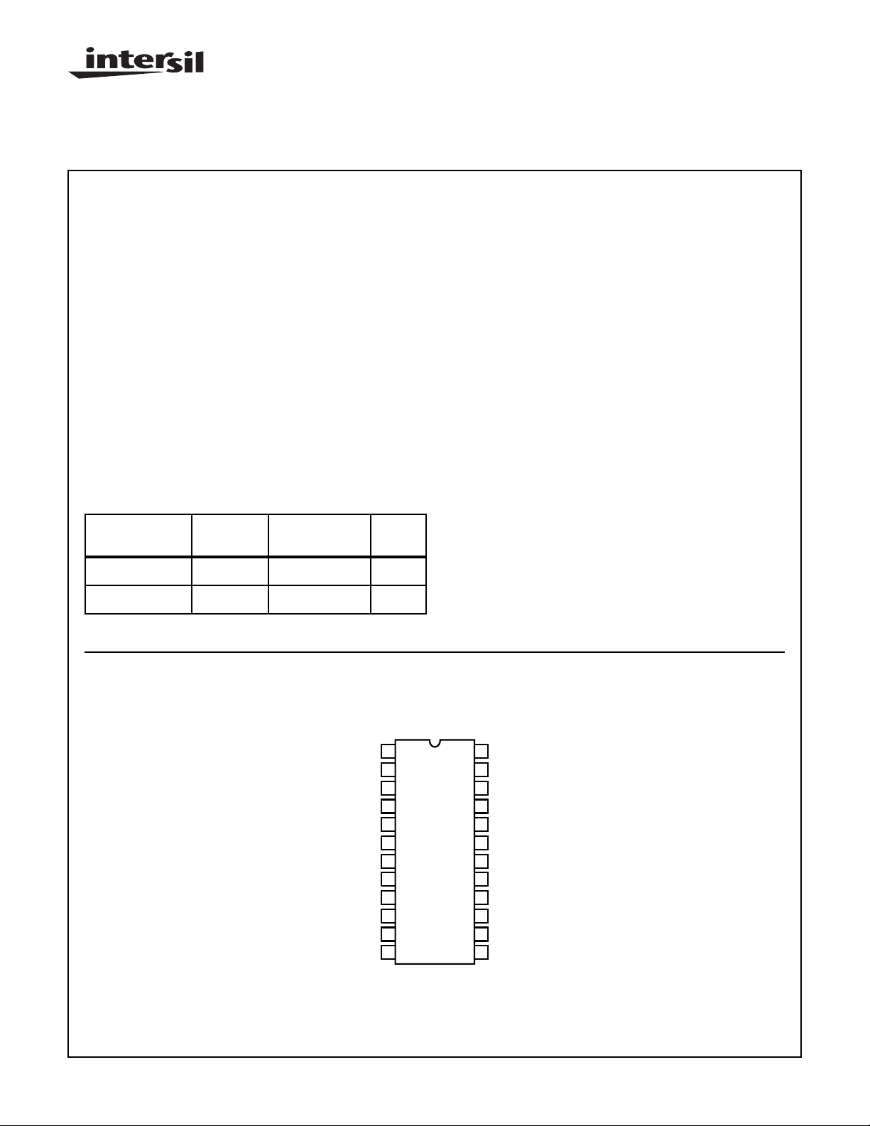
Ordering Information
TEMP.
PART NUMBER
HI3-DAC80V-5 0 to 75 24 Ld PDIP E24.6
HI3-DAC85V-4 -25 to 85 24 Ld PDIP E24.6
RANGE (oC) PACKAGE
12-Bit, Low Cost, Monolithic D/A Converters
Description
The Hl-DAC80V is a monolithic direct replacement for the
popular DAC80 and AD DAC80. The HI-DAC85V is a monolithic direct replacement for the popular DAC85 and AD
DAC85 as well as the HI-5685V. Single chip construction
along with several design innovations make the Hl-DAC80V
the optimum choice for low cost, high reliability applications.
Intersil’ unique Dielectric Isolation (Dl) processing reduces
internal parasitics resulting in fast switching times and minimum glitch. On board span resistors are provided for good
tracking over temperature, and are laser trimmed to high
accuracy.
Internally the Hl-DAC80V/HI-DAC85V eliminates code
dependent ground currents by routing current from the positive supply to the internal ground node, as determined by an
auxiliary R2R ladder. This results in a cancellation of code
dependent ground currents allowing virtually zero variation
in current through the package common, pin 21.
PKG.
NO.
The Hl-DAC80V is available as a voltage output device which
is guaranteed over the 0
HI-DAC85V is available as a voltage output device which is
guaranteed over the -25
includes a buried zener reference featuring a low temperature
coefficient as well as an on board operational amplifier. The
Hl-DAC80V requires only two power supplies and will operate
in the range of ± (11.4V to 16.5V).
o
C to 75oC temperature range. The
o
C to 85oC temperature range. It
Pinout
HI-DAC80V/HI-DAC85V
(PDIP)
TOP VIEW
(MSB) BIT 1
(LSB) BIT 12
CAUTION: These devices are sensitive to electrostatic discharge; follow proper IC Handling Procedures.
http://www.intersil.com or 407-727-9207
| Copyright © Intersil Corporation 1999
BIT 2
BIT 3
BIT 4
BIT 5
BIT 6
BIT 7
BIT 8
BIT 9
BIT 10
BIT 11
1
2
3
4
5
6
7
8
9
10
11
12
10-1034
24
6.3V REF OUT
GAIN ADJUST
23
+V
22
S
21
COMMON
∑ JUNCTION
20
19
20V RANGE
10V RANGE
18
17
BIPOLAR OFFSET
REF INPUT
16
15
V
OUT
14
-V
S
13
NC
File Number 3110.1
Page 2
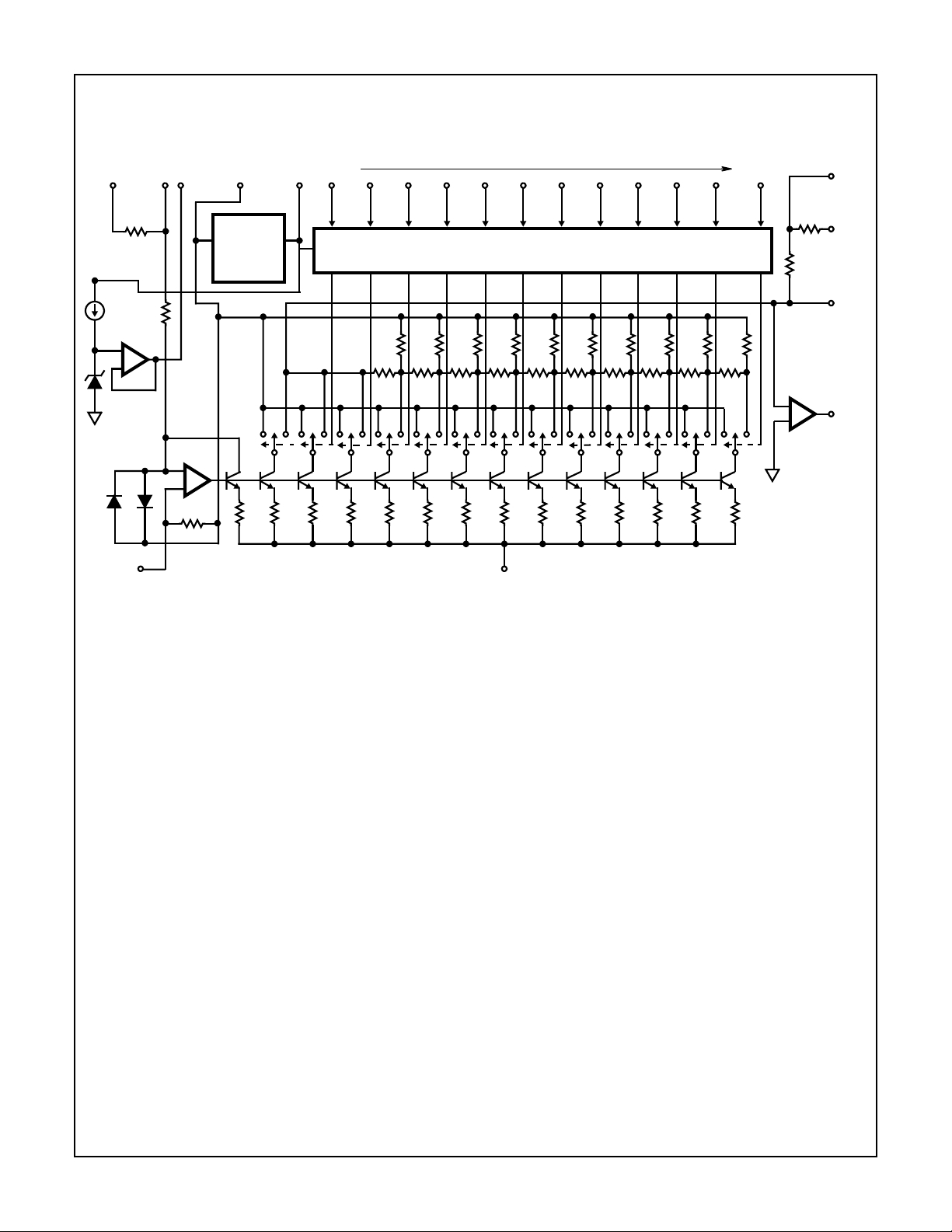
Functional Block Diagram
HI-DAC80V, HI-DAC85V
BIPOLAR
OFFSET
6.3K
12.6K
+
-
CONTROL
AMP
GAIN
ADJUST
REF
OUT COMMON
IN
+
-
12.6K
GROUND
CURRENT
CANCEL-
LATION
CIRCUIT
8K
+V
S
BIT 1 IN
(MSB)
DIGITAL INPUT LEVEL SHIFTERS AND SWITCH DRIVERS
2K
2K
2K
2K
2K
2K
2K
1K
1K
1K
1K
1K
1K
1K
8K
8K
8K
8K
8K
8K
8K8K8K
-V
S
8K
1K
2K
8K
1K
2K
8K
BIT 12 IN
1K
1K
(LSB)
8K
5K
5K
SPAN Σ
JUNCTION
-
+
10V
SPAN R
20V
SPAN R
V
OUT
10-1035
Page 3
HI-DAC80V, HI-DAC85V
Absolute Maximum Ratings Thermal Information
Power Supply Inputs
+VS. . . . . . . . . . . . . . . . . . . . . . . . . . . . . . . . . . . . . . . . . . . . +20V
-VS . . . . . . . . . . . . . . . . . . . . . . . . . . . . . . . . . . . . . . . . . . . . .-20V
Reference
Input (Pin 16) . . . . . . . . . . . . . . . . . . . . . . . . . . . . . . . . . . . . . +V
Output Drain . . . . . . . . . . . . . . . . . . . . . . . . . . . . . . . . . . . . 2.5mA
Digital Inputs (Bits 1 to 12) . . . . . . . . . . . . . . . . . . . . . . . .-1V to +V
Operating Conditions
Operating Temperature Range
HI-DAC80V. . . . . . . . . . . . . . . . . . . . . . . . . . . . . . . . .0oC to 75oC
HI-DAV85V . . . . . . . . . . . . . . . . . . . . . . . . . . . . . . . -25oC to 85oC
CAUTION: Stresses above those listed in “Absolute Maximum Ratings” may cause permanent damage to the device. This is a stress only rating and operation
of the device at these or any other conditions above those indicated in the operational sections of this specification is not implied.
NOTE:
1. θJA is measured with the component mounted on an evaluation PC board in free air.
Thermal Resistance (Typical, Note 1) θJA (oC/W)
PDIP Package. . . . . . . . . . . . . . . . . . . . . . . . . . . . . 60
Maximum Power Dissipation
PDIP Package. . . . . . . . . . . . . . . . . . . . . . . . . . . . . . . . . . 550mW
S
Maximum Junction Temperature . . . . . . . . . . . . . . . . . . . . . . .150oC
Maximum Storage Temperature Range . . . . . . . . . .-65oC to 150oC
S
Maximum Lead Temperature (Soldering 10s). . . . . . . . . . . . . 300oC
Die Characteristics
Process. . . . . . . . . . . . . . . . . . . . . . . . . . . . . . . . . . . . . . . Bipolar-DI
Transistor Count . . . . . . . . . . . . . . . . . . . . . . . . . . . . . . . . . . . . . 214
Electrical Specifications T
PARAMETER TEST CONDITIONS
SYSTEM PERFORMANCE
Resolution - - 12 Bits
ACCURACY (Note 2)
Linear Error Full Temperature - ±
Differential Linearity Error Full Temperature - ±1/
Monotonicity Full Temperature Guaranteed
Gain Error Full Temperature (Notes 1, 3) - ±0.1 ±0.3 % FSR
Offset Error Full Temperature (Note 1) ±0.05 ±0.15 % FSR
ANALOG OUTPUT
Output Ranges - ±2.5 - V
Output Current ±5- -mA
Output Resistance - 0.05 - Ω
Short Circuit Duration To Common Continuous DRIFT (Note 2)
Total Bipolar Drift (Includes Gain,
Offset and Linearity Drifts)
Total Error
Unipolar Full Temperature (Note 5) - ±0.08 ±0.15 % FSR
Bipolar Full Temperature (Note 5) - ±0.06 ±0.1 % FSR
Gain With Internal Reference - ±15 ±30 ppm/
Unipolar Offset - ±1 ±3 ppm/oC
Bipolar Offset - ±5 ±10 ppm/oC
CONVERSION SPEED
Settling Time Full Scale Transition All Bits ON
With 10K Feedback - 3 - µs
With 5K Feedback - 1.5 - µs
For 1 LSB Change - 1.5 - µs
= 25oC, VS ±12V to ±15V (Note 4), Pin 16 to Pin 24, Unless Otherwise Specified
A
HI-DAC80V-5, HI-DAC85V-5
UNITSMIN TYP MAX
1
/
4
2
- ±5- V
- ±10 - V
- 0 to 5 - V
- 0 to 10 - V
Full Temperature - - ±20 ppm/oC
Without Internal Reference - ±7 - ppm/oC
to OFF or OFF to ON to ±0.01%
or FSR (Note 2)
±1/
±3/
2
4
LSB
LSB
o
C
10-1036
Page 4

HI-DAC80V, HI-DAC85V
Electrical Specifications T
PARAMETER TEST CONDITIONS
Slew Rate 10 15 - V/µs
INTERNAL REFERENCE
Output Voltage 6.250 +6.3 6.350 V
Output Impedance - 1.5 - Ω
External Current - - +2.5 mA
Tempco of Drift - 5 - ppm/oC
DIGITAL INPUT (Note 2)
Logic Levels
Logic “1” TTL Compatible At +1µA +2 - +5.5 V
Logic “0” TTL Compatible At -100µA 0 - +0.8 V
POWER SUPPLY SENSITIVITY (Notes 2, 4)
+15V Supply - 0.001 0.002 % FSR / %V
-15V Supply - 0.001 0.002 % FSR / %V
POWER SUPPLY CHARACTERISTICS (Note 4)
Voltage Range
+V
S
-V
S
Current
+I
S
-I
S
NOTES:
1. Adjustable to zero using external potentiometers.
2. See Definitions.
3. FSR is “Full Scale Range: and is 20V for±10V range, 10V for ±5V range, etc.
4. The HI-DAC80V/HI-DAC85V will operate with supply voltages as low as±11.4V. It is recommended that output v oltage r ange -10V to
+10V not be used if the supply voltages are less than ±12.5V.
5. With Gain and Offset errors adjusted to zero at 25oC.
= 25oC, VS ±12V to ±15V (Note 4), Pin 16 to Pin 24, Unless Otherwise Specified (Continued)
A
HI-DAC80V-5, HI-DAC85V-5
UNITSMIN TYP MAX
Full Temperature +11.4 +15 +16.5 V
Full Temperature -11.4 -15 -16.5 V
Full Temperature, VS = ±15V - +12 +15 mA
Full Temperature, VS = ±15V - -15 -20 mA
S
S
Definitions of Specifications
Digital Inputs
The Hl-DAC80V accepts digital input codes incomplementary
binary, complementary offset binary, and complementary
two’s complement binary.
Settling Time
That interval between application of a digital step input, and
final entry of the analog output within a specified window
about the settled value. Intersil Corporation usually specifies
a unipolar 10V full scale step, to be measured from 50% of
the input digital transition, and a window of ±
the final value. The device output is then rated according to
the worst (longest settling) case: low to high, or high to low.
In a 12-bit system ±
1
/2 LSB = ±0.012% of FSR.
1
/2 LSB about
10-1037
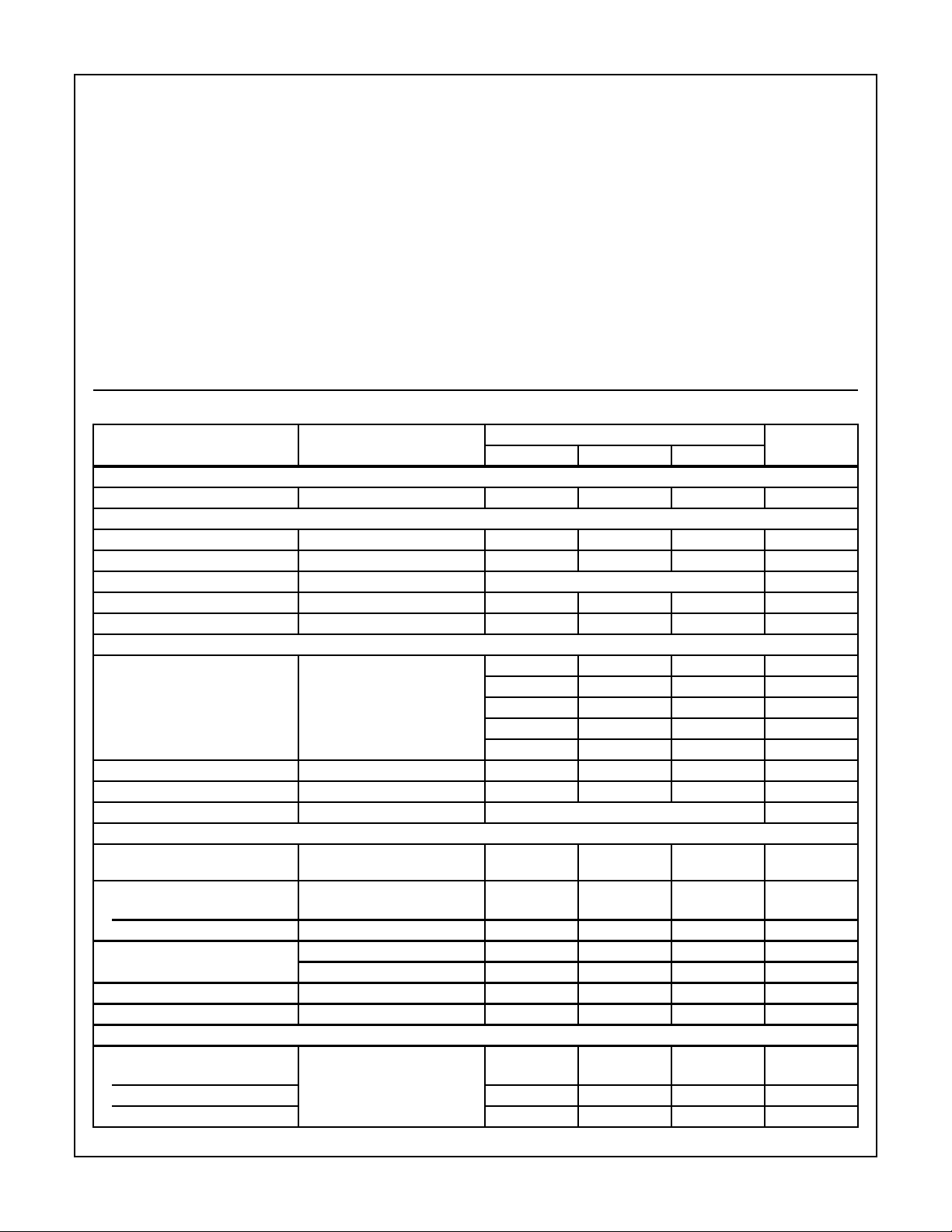
TABLE 1.
ANALOG OUTPUT
COMPLE-
MENTARY
DIGITAL
INPUT
MSB...LSB
000...000 + Full Scale + Full Scale -LSB
100...000 Mid Scale-1 LSB -1 LSB + Full Scale
111...111 Zero - Full Scale Zero
011...111 +1/2 Full Scale Zero - Full Scale
STRAIGHT
BINARY
COMPLE-
MENTARY
OFFSET
BINARY
COMPLE-
MENTARY
TWO’S
COMPLEMENT†
†Invert MSB with external inverter to obtain CTC Coding
Page 5

HI-DAC80V, HI-DAC85V
Thermal Drift
o
Thermal drift is based on measurements at 25
(T
) and low (TL) temperatures. Drift calculations are made
H
for the high (T
-25oC) and low (25oC-TL) ranges, and the
H
C, at high
larger of the two values is given as a specification representing worst case drift.
Gain Drift, Offset Drift, Reference Drift and Total Bipolar Drift
are calculated in parts per million per
∆FSR ∆°C⁄
GainDrift
OffsetDrift
ReferenceDrift
TotalBipolarDrift
NOTE: FSR = Full Scale Output Voltage - Zero Scale Output
∆FSR = FSR (TH) - FSR (25oC),
or FSR (25
V
= Steady State response to any input code.
O
--------------------------------
Voltage
o
C) - FSR (TL).
FSR
∆Offset ∆°C⁄
-------------------------------------
FSR
∆V
REF
---------------------------------------
V
REF
∆VO∆°C()⁄
--------------------------------
FSR
106×=
106×=
∆°C()⁄
o
C as follows:
6
×=
10
6
×=
10
Total Bipolar Drift is the variation of output voltage with
temperature, in the bipolar mode of operation. It represents
the net effect of drift in Gain, Offset, Linearity and Reference
Voltage. Total Bipolar Drift values are calculated, based on
measurements as explained above. Gain and Offset need
not be calibrated to zero at 25
o
C. The specified limits for
TBD apply for any input code and for any power supply setting within the specified operating range.
Accuracy
values within the specified operating range. Gain and offset
errors must be calibrated to zero at 25
o
C. Then the specified
limits for Total Error apply for any input code and for any
temperature within the specified operating range.
Power Supply Sensitivity
Power Supply Sensitivity is a measure of the change in gain
and offset of the D/A converter resulting from a change in
-V
, or +VS supplies. It is specified under DC conditions and
S
expressed as full scale range percent of change divided by
power supply percent change.
∆FullScaleRange 100×
-------------------------------------------------------------------
PSS
FSR Nominal()
-------------------------------------------------------------------=
100×
∆V
S
--------------------------------- -
(Nominal)
V
S
Glitch
A glitch on the output of a D/A converter is a transient spike
resulting from unequal internal ON-OFF switching times.
Worst case glitches usually occur at half-scale, i.e., the
major carry code transition from 011...1 to 100...0 or vice
versa. For example, if turn ON is greater than OFF for
011...1 to 100...0, an intermediate state of 000...0 exists,
such that, the output momentarily glitches toward zero output. Matched switching times and fast switching will reduce
glitches considerably. (Measured as one half the Product of
duration and amplitude.)
Decoupling and Grounding
For best accuracy and high frequency performance, the
grounding and decoupling scheme shown in Figure 1 should
be used. Decoupling capacitors should be connected close
to the HI-DAC80V/HI-DAC85V (preferably to the device pins)
and should be tantalum or electrolytic bypassed with
ceramic types for best high frequency noise rejection.
Linearity Error (Short for “Integral Linearity Error.” Also,
sometimes called “Integral Nonlinearity” and “Nonlinearity”.)
The maximum deviation of the actual transfer characteristic
from an ideal straight line. The ideal line is positioned
according to end-point linearity for D/A converter products
from Intersil Corporation , i.e., the line is drawn between the
end-points of the actual transfer characteristic (codes 00...0
and 11...1).
Differential Linearity Error The difference between one
LSB and the output voltage change corresponding to any
two consecutive codes. A Differential Nonlinearity of ±1 LSB
or less guarantees monotonicity.
Monotonicity The property of a D/A converter’s transfer
function which guarantees that the output derivative will not
change sign in response to a sequence of increasing (or
decreasing) input codes. That is, the only output response to
a code change is to remain constant, increase for Increasing
code, or decrease for decreasing code.
Total Error The net output error resulting from all inter nal
effects (primarily non-ideal Gain, Offset, Linearity and
Reference Voltage). Supply voltages may be set to any
10-1038
-V
S
0.01µF
1µF
14 21 22
24
16
FIGURE 1.
0.01µF
1µF
+V
S
18
19
20
-
+
15
Page 6

HI-DAC80V, HI-DAC85V
Reference Supply
An internal 6.3V reference is provided on board the
HI-DAC80V/HI-DAC85V. The voltage (pin 24) is accurate to
±0.8% and must be connected to the reference input (pin 16)
for specified operation. This reference may be used externally, provided current drain is limited to 2.5mA. An external
buffer amplifier is recommended if this reference is to be
used to drive other system components. Otherwise, variations in the load driven by the reference will result in gain
variations of the HI-DAC80V/HI-DAC85V. All gain adjustments should be made under constant load conditions.
Output Voltage Ranges
+V
S
R1
2.8MΩ
-V
S
10kΩ TO
100kΩ
24
17
16
23
0.01µF
6.3K
12.6kΩ
CONTROL
AMP
18
5kΩ
5kΩ
-
+
19
20
15
21
-
+
3.9
MΩ
+V
R2
-V
5kΩ
TO
100kΩ
TABLE 3. GAIN AND OFFSET CALIBRATIONS
UNIPOLAR CALIBRATION
Step 1: Offset
Turn all bits OFF (11 . . . 1)
Adjust R2 for 0V out
Step 2: Gain
Turn all bits ON (00 . . . 0)
Adjust R1 for FS - 1 LSB
That is:
4.9988 for 0 to +5V range
9.9976 for 0 to +10V range
BIPOLAR CALIBRATION
Step 1: Offset
S
Turn all bits OFF (11 . . . 1)
Adjust R2 for Negative FS
That is:
-10V for ±10V range
-5V for ±5V range
S
-2.5V for ±2.5V range
Step 2: Gain
Turn all bits ON (00 . . . 0)
Adjust R1 for Positive FS - 1 LSB
That is:
+9.9951V for ±10V Range
+4.9976V for ±5V Range
+2.4988V for ±2.5V Range
This Bipolar procedure adjusts the output range end points. The
maximum error at zero (half scale) will not exceed the Linearity
Error. See the “Accuracy” Specifications.
FIGURE 2. HI-DAC80V/HI-DAC85V
TABLE 2. RANGE CONNECTIONS
CONNECT
RANGE
PIN 15 PIN 17 PIN 19
Unipolar 0 to +5V 18 NC 20
0 to +10V 18 NC NC
Bipolar ±2.5V 18 20 20
±5V 18 20 NC
±10V 19 20 15
10-1039
Page 7

Die Characteristics
HI-DAC80V, HI-DAC85V
DIE DIMENSIONS:
108 mils x 163 mils
METALLIZATION:
Type: Al
Thickness: 16k
Å ±2kÅ
TIE SUBSTRATE TO:
Ground
Metallization Mask Layout
BIT 3 BIT 2
BIT 4
PASSIVATION:
Type: Nitride over Silox
Nitride Thickness: 3.5k
Silox Thickness: 12kű1.5kÅ
WORST CASE CURRENT DENSITY:
0.95 x 10
HI-DAC80V, HI-DAC85V
BIT 1
(MSB)
6.3V
REF OUT GAIN ADJUST
5
A/cm
2
Å ±0.5kÅ
+V
S
COMMON
SUMMING JUNCTION
BIT 5
BIT 6
BIT 7
BIT 8
BIT 9
BIT 10
BIT 12BIT 11
-V
S
V
20V
SPAN
10V
SPAN
BIPOLAR
OFFSET
REF IN
OUT
All Intersil semiconductor products are manufactured, assembled and tested under ISO9000 quality systems certification.
Intersil products are sold by description only. Intersil Corporation reserves the right to make changes in circuit design and/or specifications at any time without
notice. Accordingly, the reader is cautioned to verify that data sheets are current before placing orders. Information furnished by Intersil is believed to be accurate
and reliable. However, no responsibility is assumed by Intersil or its subsidiaries for its use; nor for any infringements of patents or other rights of third parties which
may result from its use. No license is granted by implication or otherwise under an y patent or patent rights of Intersil or its subsidiaries.
For information regarding Intersil Corporation and its products, see web site http://www.intersil.com
10-1040
 Loading...