

January2001
HI-8787,HI-8788
DESCRIPTION
TheHI-8787andHI-8788aresystemcomponentsfor
interfacing16bitparalleldatatoanARINC429bus.They
combinelogicandlinedriverononechip.TheHI-8787has
anoutputresistanceof37.5ohms,andtheHI-8788has
outputresistanceof10ohmstofacilitateexternallightning
protectioncircuitry. Thetechnologyisanalog/digital
CMOS.
Bothproductsofferhighspeeddatabustransactionsintoa
bufferregister.Afterloading216-bitwords,datais
automaticallytransferredandtransmitted.Thedatarateis
equaltotheclockrate.Paritycanbeenabledinthe32nd
bit.Resetisusedtoinitializethelogicuponstartup.Word
gapsareautomaticallysent.
Thepartrequires+/-10voltsuppliesinadditiontoa5volt
supply.
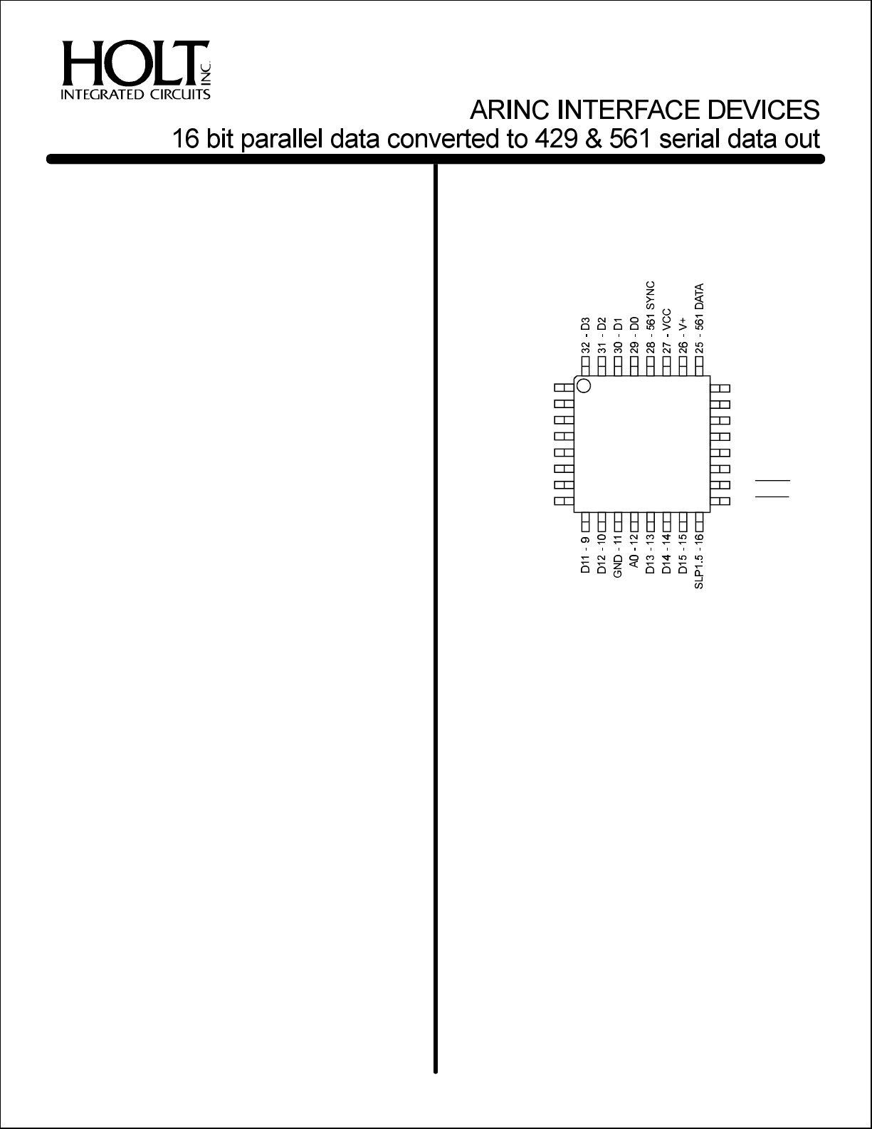
PINCONFIGURATION
D4-1
N/C-2
D5-3
D6-4
D7-5
D8-6
D9-7
D10-8
HI-8787PQI
HI-8787PQT
HI-8788PQI
&
HI-8788PQT
24-TXBOUT
23-TXAOUT
22-V21-PARITYENB
20-XMTRDY
19-XMITCLK
18-
RESET
17-
WRITE
FEATURES
l
l
l
l
l
Automaticallyconverts16bitparalleldata
toARINC429or561data
Highspeeddatabusinterface
On-chiplinedriver
AvailableinsmallTQFPpackage
Militaryprocessingoptions
32-PinPlasticTQFPpackage
HOLTINTEGRATEDCIRCUITS
(DS8787Rev.B)01/01
1
HI-8787,HI-8788
PINDESCRIPTIONS
PINSYMBOLFUNCTIONDESCRIPTION
28561SYNCdigitaloutputARINC561Syncsignal
1,3-10,13-15,29-32DndigitalinputsParallel16bitbusinput
11GNDpowersupplyGround
12A0digitalinputLoadaddress,A0=0for1stdataload,A0=1for2nddataload
16SLP1.5digitalinputSelectstheslopeofthelinedriver.High=1.5us
17digitalinputWritestrobe.Loadsdataonrisingedge.
18digitalinputRegistersandsequencinglogicinitializedwhenlow
19XMITCLKdigitalinputClockinputforthetransmitter
20XMTRDYdigitaloutputGoeshighifthebufferregisterisempty
21PARITYENBdigitalinputWhenhighthe32ndbitoutputi soddparity
22V-powersupply-10voltrail
23TXAOUTanalogoutputLinedriveroutput-Aside
24TXBOUTanalogoutputLinedriveroutput-Bside
25561DATAdigitaloutputSerialoutputforARINC561data
26V+powersupply+10voltrail
27VCCpowersupply+5voltrail,“one”leveloutoflinedriver,invertedfor“zero”
WRITE
RESET
FUNCTIONALDESCRIPTION
TheHI-8787isaparalleltoserialconverter,whichwhen
loadedwithtwo16bitparallelwords,outputsthedataasa
32bitserialword.Timingcircuitryinsertsa4bitgapatthe
endofeach32bitword.Aninputbufferregisterallowsload
operationstotakeplacewhilethepreviouslyloadedword
isbeingtransmitted.
IfthePARITYENBpinishigh,the32ndbitwillbeaparity
bit,insertedsoastomakethe32bitwordhaveoddparity.If
thePARITYENBpinislow,the32ndbitwillbetheD15bit
ofthe2ndwordloaded.
OutputsareprovidedforbothARINC429(TXAOUTand
TXBOUTpins),andARINC561(561DA TAand561SYNC
pins)typedata.
AlowsignalappliedtothepinresetstheHI-8787’s
internallogicsothatspurioustransmissiondoesnottake
placeduringpower-up.Theregistersareclearedsothata
continuousgapwillbetransmitteduntilthefirstwordis
loadedintothetransmitter.
TheXMITCLKfrequencyisthesameasthedatarate.
RESET
InputdatacanbeloadedwhentheXMTRDYsignalis
high,whichindicatestheinputbufferregisterisempty.The
first16bitwordisloadedwiththeA0inputhigh.ThesecondwordisloadedwithA0inthelowstate.Eachdataword
isloadedintotheinputbufferregisterbyalowpulseonthe
WRITE
input.(Seefigure1).Afterthesecondwordhas
beenloaded,theXMTRDYoutputgoeslow.Thecontents
oftheinputbufferregisteraretransferredtotheoutputregisterduringthefourthbitperiodofthegap.Ifthefourthgap
bitperiodofthepreviouswordhasalreadybeentransmitted,thecontentsoftheinp utbufferregisterwillbetransferredtotheoutputshiftregisterduringthefirstbitperiodaftertheseconddataload,andtheXMTRDYoutputgoes
high.
Aftertheoutputshiftregisterisloaded,thedataisshifted
outtotheoutputlogicintheordershowninfigure2.
The561SYNCoutputpulseslowwhentheXMITCLKis
lowduringthe8thbitoftheARINCtransmission.
HOLTINTEGRATEDCIRCUITS
HOLTINTEGRATEDCIRCUITS
2
2
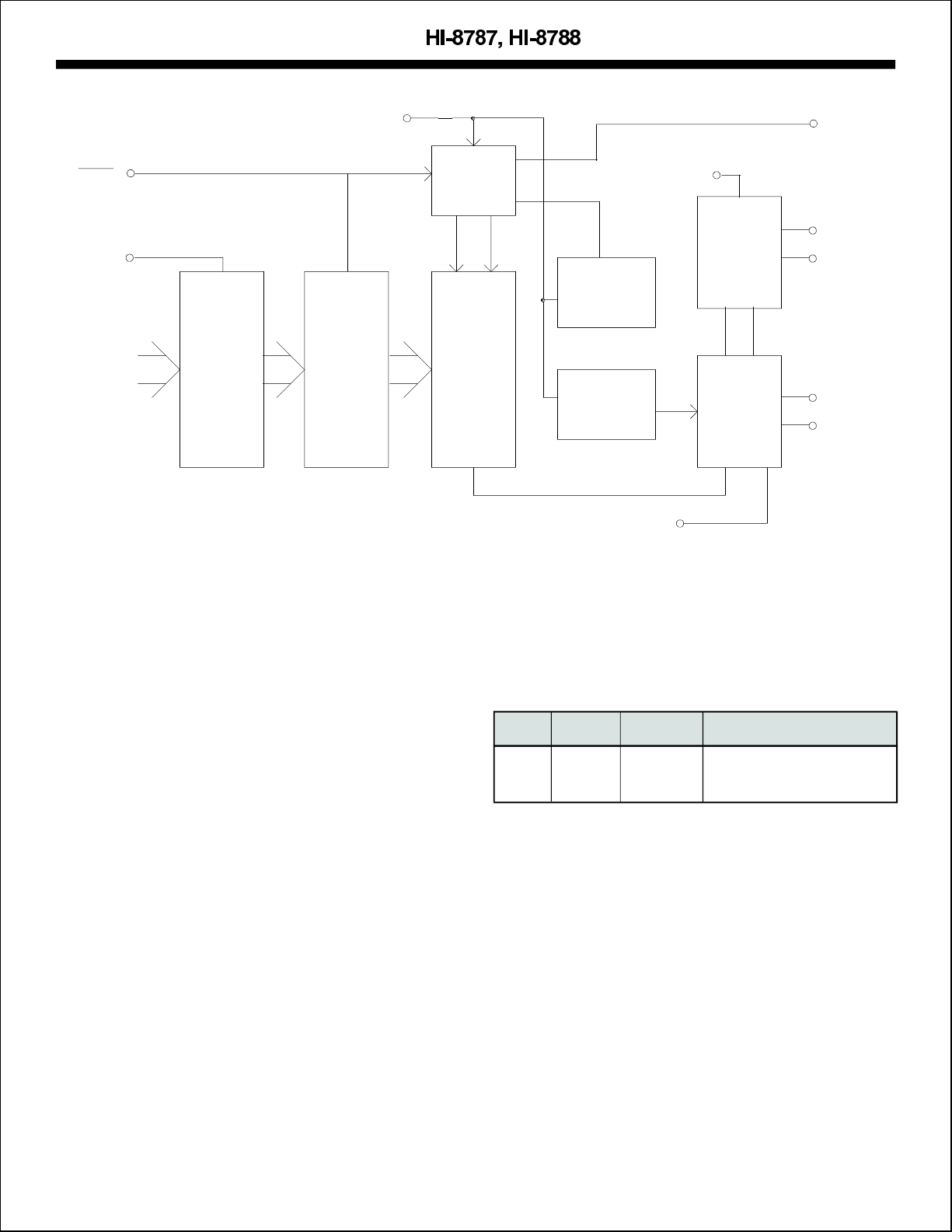
XMITCLK
XMTRDY
WRITE
DATA
BUS
status&
control
logic
A0
wordgap
counter
16
16to32bit
mux
32 32
32bit
buffer
register
32bit
shift
register
bit
counter
PARITYENB
SLP1.5
line
driver
output
logic
TXAOUT
TXBOUT
561SYNC
561DATA
Figure1.BlockDiagram
FUNCTIONALDESCRIPTION(Cont.)
TheHI-8787andHI-8788haveanon-chiplinedriverdesignedtodirectlydrivetheARINC429bus.ThetwoARINC
outputs(TXAOUTandTXBOUT)provideadifferentialvoltagetoproducea+10voltOne,a-10voltZero,anda0volt
Null.TheslopeoftheARINCoutputsiscontrolledbythe
SLP1.5pin.IfSLP1.5ishigh,theoutputriseandfalltimeis
nominally1.5s..IfSLP1.5issetlow,theriseandfalltimes
are10s.
µ
TheHI-8787has37.5ohmsinserieswitheachlinedriver
output.TheHI-8788has10.0ohmsinseries.TheHI-8788
isforapplicationswhereexternalseriesresistanceis
needed,typical lyforlightningprotectiondevices.
µ
A0LoadDataBusARINCBits
1Word1D0-D15ARINC1-ARINC16
0Word2D0-D15ARINC17-ARINC32
Figure2.Orderoftransmitteddata
HOLTINTEGRATEDCIRCUITS
3

XMITCLK
561DATA
561SYNC
ARINC429DATA
(TXAOUT-TXBOUT)
353612345313233343536
LOWDURINGCLK8
XMTCLK
t
phlx
t
plhx
trxt
10%
t
plhx
t
phlx
t
rx
90%
90%
10%
10%
tt
fx
HOLTINTEGRATEDCIRCUITS
4
10V
0V
-10V
tfxt

ABSOLUTEMAXIMUMRATINGS
RECOMMENDEDOPERATINGCONDITIONS
VoltagesreferencedtoGround
SupplyVoltages
V+.......................................+10V...±5%
Supplyvoltages
V+.................................................12.5V
V-........................................-10V...±5%
VCC.......................................5V...±5%
V-.................................................-12.5V
VCC..................................................7V
TemperatureRange
DCcurrentperinputpin................+10ma
IndustrialScreening.........-40°Cto+85°C
Hi-TempScreening........-55°Cto+125°C
Powerdissipationat25°
MilitaryScreening..........-55°Cto+125°C
plasticDIL............1.0W,derate10mW/°C
ceramicDIL..........0.5W,derate7mW/°C
NOTE:Stressesaboveabsolutemaximum
ratingsoroutsiderecommendedoperating
SolderTemperature........275°Cfor10sec
conditionsmaycausepermanentdamagetothe
device.Thesearestressratingsonly.Operation
StorageTemperature........-65°Cto+150°C
VCC=5.0V,V=0V,V+=10V,V-=-10V,T=OperatingTemperatureRange(unlessotherwisespecified).SSA
PARAMETERSYMBOLCONDITIONMINTYPMAXUNITS
OperatingVoltageV4.7555.25V
OperatingVoltageV+9.51010.5V
OperatingVoltageV--9.5-1010.5V
Min.InputVoltage(HI)V2.01.4V
Max.InputVoltage(LO)V1.40.7V
Min.InputCurrent(HI)IV=4.9V280µA
Max.InputCurrent(LO)IV=0.1V-1µA
Min.OutputVoltage(HI)VI=-1.6mA2.7V
Max.OutputVoltage(LO)VI=1.6mA0.4V
LineDriverOutputLevels(Ref.ToGND)
ONEnoload,VCC=5.0V4.55.05.5V
NULL“-0.2500.25V
ZERO-5.5-5.0-4.5V
LineDriverOutputLevels
(DifferentialTXAOUT-TXBOUT)
ONEnoload,VCC=5.0V9.010.011.0V
NULL“-0.500.5V
ZERO“-11.0-10.0-9.0V
MinimumShortCircuitSinkorSourceCurrentImomentarymagnitude80mA
OperatingCurrentDrainIf=100khz0.82.8mA
OperatingCurrentDrain(V+)If=100khz620mA
OperatingCurrentDrain(V-)If=100khz-20-6mA
InputCapacitanceCNottested20pF
CC
IH
IL
IHIH
ILIL
OHOUT
IHOUT
OUT
CC
DD
EE
IN
atthelimitsisnotrecommended.
HOLTINTEGRATEDCIRCUITS
5

VCC=5.0V,V+=10V,V-=-10V,V=0V,T=OperatingTemperatureRange(unlessotherwisespecified).SSA
PARAMETERSYMBOLTESTCONDITIONSMINTYPMAXUNITS
DATABUSTIMING
SetupDataBustons
Hold0ns
WRITE
HoldA0to0ns
Pulsewidth40ns
PulsewidthA040ns
Delaylast40ns
LINEDRIVERTIMING
LineDriverpropagationdelayNoload
Outputhightolowtphlx-500-ns
Outputlowtohightplhx-500-ns
LineDrivertransitiontimes
OutputhightolowtfxSLP1.5=logic11.01.52.0s
OutputlowtohightrxSLP1.5=logic11.01.52.0s
toDataBus
WRITE
WRITE
WRITE
WRITE SET
toXMTRDY
t20
t
HLD
t
AH
t
WPW
t
APW
t
XD
µ
µ
OutputhightolowtfxSLP1.5=logic051015s
OutputlowtohightrxSLP1.5=logic051015s
µ
µ
ORDERINGINFORMATION
HI-8787PQIYES37.5ohm32PinPlasticTQFP-40°CTO+85°CISOLDER
HI-8787PQTYES37.5ohm32PinPlasticTQFP-55°CTO+125°CTSOLDER
HI-8788PQIYES10.0ohm32PinPlasticTQFP-40°CTO+85°CISOLDER
HI-8788PQTYES10.0ohm32PinPlasticTQFP-55°CTO+125°CTSOLDER
HOLTINTEGRATEDCIRCUITS
6

HI-8787,HI-8788PACKAGEDIMENSIONS
32PINPLASTICTHINQUADFLATPACK(TQFP)
.00057.00022±
(0.0145 ±).0055
.3543BSC
(9.00BSC )
SQ.
.2755BSC
(7.00BSC )
SQ.
.0315BSC
(0.80BSC )
.0148.0030±
(0.375 ±).075
.0236.0059±
(0.60 ±).15
inches(millimeters)
PackageType:
32PTQS
.063MAX.
(1.60MAX. )
SeeDetailA
.0551.002±
(1.4 ± .05)
.0039.002±
(0.10 ±).05
.0055R.0024±
(0.14R ±).06
0°7°≤Θ≤
.0031RMIN.
(0.08RMIN. )
DetailA
HOLTINTEGRATEDCIRCUITS
7
 Loading...