


HI-8050/51,HI-8150/51
January2001
CMOSHIGHVOLTAGEDISPLAYDRIVER
GENERALDESCRIPTION
TheHI-8050,HI-8051,HI-8150andHI-8151areCMOS
integratedcircuitsdesignedforhighvoltageLCDdisplay
driveapplications.TheHI-8050&HI-8051haveTTLlogic
inputswhereastheHI-8150&HI-8151haveCMOSlogic
inputs.Theydriveupto38segmentsatvoltagesbetween
+5and-30volts.Theoptionalnegativeconverteronthe
HI-8050&HI-8150canbeusedtogeneratethenegative
displaydrivevoltage.Allproductshavetestinputsto
facilitateopensandshortstestingaswellasautomatic
blankingofthedisplayifthe+5Vpowerislost.
TheHI-8050andHI-8150aredesignedtoreplacet he
HI-8010andHI-8020devicesinall5voltapplications.They
offersignificantlyenhancedESDprotectionalongwitha
considerablyfasterserialinputdatarate.
Thedataisseriallyclockedintothedeviceonthenegative
edgeoftheclockandlatchedinparalleltothesegment
outputsonthehightolowtransitionoftheloadinput.Serial
outputdatachangesonthepositiveedgeoftheclock
allowingthecascadingofmultipledriversforlargerdisplays.
Thedevicelayoutsupportsallpreviouspinoutsofthe
HI-8010/HI-8020products.Inaddition,newtechnologyand
featuresaffordne wpackagingoptions.ConsultyourHolt
SalesRepresentativetoexplorethepossibilities.
APPLICATIONS
!
DichroicLiquidCrystalDisplays
!
StandardLiquidCrystalDisplays
! 5VoltSerialDatatoParallelHighVoltage
PADCONFIGURATION (TopView)
BPIN
BPOSC
VDD
N/C
CONVOSC
CONVOUT
VEE
S37
S38
S1
S2
S3
S4
S5
S6
S7
(Seepage3-32AforHI-8051&HI-8151pinconfigurations)
2
3
4
5
6
7
8
9
10
11
12
13
14
15
16
HI-8050PQI
HI-8150PQI
HI-8050PQT
&
HI-8150PQT
48
47
46
45
44
43
42
41
40
39
38
37
36
35
34
S27
S26
S25
S24
S23
S22
S21
S20
DOUT38
DOUT32
DOUT30
T2
T1
N/C
BPOUT
N/C
FEATURES
!
4MHzserialinputdatarate
!
38segmentoutputs
!
Cascadable
!
5Voltinputstranslatedto35Volts
!
Testpinsallowhardwareall"ON",all"OFF"or
alternating
!
Monitors5voltsupplyandforcesall
segmentsto"OFF"conditioniflost
!
Negativevoltageconverteravailableon-chip
!
CMOSlowpower
!
Militaryprocessingavailable
HOLTINTEGRATEDCIRCUITS
FUNCTIONALBLOCKDIAGRAM
DIN
Þ
Þ
CL
Þ
CS
8020OPT Þ
LD
BPIN
BPOSC
Þ
Þ
Þ
CONTROL
LOGIC
Oscillator
Divider
Voltage
Translator
HighVoltage
Buffer
Þ BPOUT
1(DS8050Rev.C)01/01
DATAIN
38Stage
ShiftRegister
CLK
LE
38BitLatch
Voltage
Translators
HighVoltage
Drivers
38SEGMENTS
DOUT38
DOUT32
DOUT30
HI-8050/51,HI-8150/51
PINDESCRIPTIONTABLE
SIGNALFUNCTIONDESCRIPTION
VSSPOWER0Volts
8020OPTCLCS
CS
CL
LDLOGICINPUTLatchesdatainshiftregistertothesegmentoutputs-Activehigh
DINLOGICINPUTSerialinputdatatotheshiftregister
BPININPUTBackplanefrequencyinput.Eitherdrivenfromanexternalsourceorconnected
BPOSCOUTPUTInternaloscillatorpin.ConnectedtoBPINandanexternalresisto randcapacitor
VDDPOWER+5V±5%,Positivevoltageofthebackplaneandsegments
CONVOSCINPUTUsedinconjunctionwithCONVOUTtogeneratethenegativeVEEvoltage
CONVOUTOUTPUTUsedinconjunctionwithCONVOSCtogeneratethenegativeVEEvoltage
VEEPOWERNegativevoltageofthebackplaneandsegments-betweenVSSandVDD-35V
LOGICINPUTOpenorhighlogiclevelselectstheHI-8010/HI-8110/logic.Alow
selectstheHI-8020/HI-8120Logic(HI-8050&HI-8150only)
LOGICINPUTChipselect-Activelow
LOGICINPUTSerialdatainputclock-Activelow
toBPOSCandanexternalresistorandcapacitor.
on-chip(HI-8050&HI-8150only).
on-chip(HI-8050&HI-8150only).
S1toS38OUTPUTSegmentoutputstoLCDdisplay
BPOUTOUTPUTBackplaneoutputtoLCDdisplay(SeeFigure3forcascadingdrivers)
T1LOGICINPUTUsedinconjunctionwithT2tocontroldisplaymod e.Normalmodeislogiclow.
T2LOGICINPUTUsedinconjunctionwithT1tocontroldisplaymode.Normalmodeislogiclow.
DOUT30OUTPUTLogicoutputfromthe30thbitoftheshiftregister.Useforpattern
verificationorastheDINofthenextcascadeddriver(HI-8050&HI-8150only).
DOUT32OUTPUT
DOUT38OUTPUT
Logicoutputfromthe32ndbitoftheshiftregister.Useforpattern
verificationorastheDINofthenextcascadeddriver(HI-8050&HI-8150only).
Logicoutputfromthe38thbitoftheshiftregister.Useforpattern
verificationorastheDINofthenextcascadeddriver.
HOLTINTEGRATEDCIRCUITS
2
FUNCTIONALDESCRIPTION
HI-8050/51,HI-8150/51
INPUTLOGIC
ThedataisclockedintoaserialshiftregisterfromtheDINinputonthenegativeedgeofwhileisheldlow.LDis
CL CS
normallyheldlowandpulsedhighonlywhendatafromthe
shiftregisterisparallellatchedtothesegmentoutputs.
CS
mustbelowwhenLDispulsed.Thelatchesaretransparent
whileLDishigh.Alogic"1"intheshiftregistercausesthe
correspondingsegmentoutputtobeoutofphasewiththe
BPoutput.AllfourlogicinputsareTTLcompatibleonthe
HI-8050/51andCMOScompatibleontheHI-8150/51.
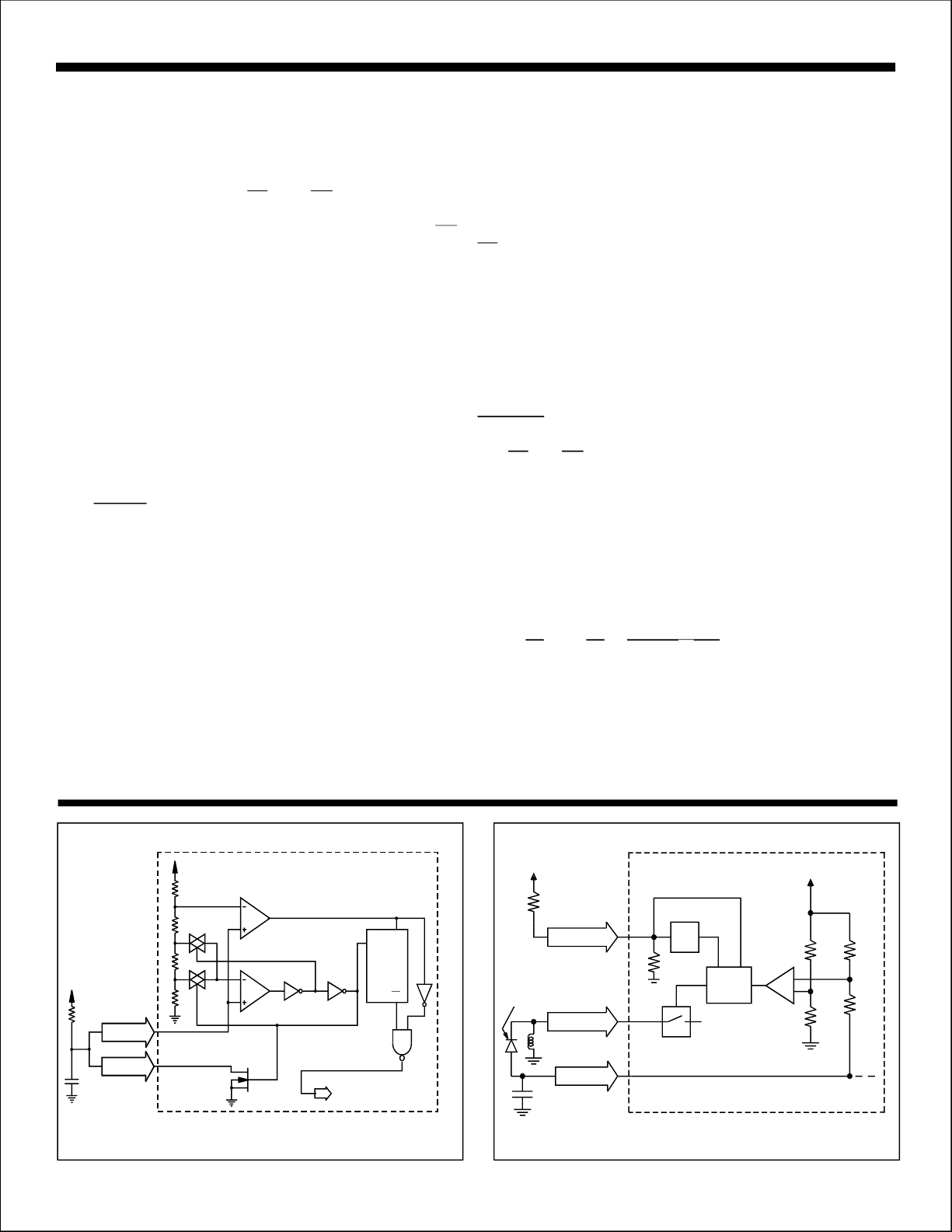
BPOSCandBPIN
Theuserhastheoptionofcreatingthebackplanefrequency
internallyorprovidingas ignalfromanexternalsource.For
aninternaloscillator,BPINandBPOSCareconnectedtogetherandtheappropriateR&Ccombinationisappliedas
showninFigure1.Theresultingbackplanefrequencyisapproximately:
f=1.(R=220K,C=220pF,f100HZ)
BPBP
256RC
Thevalueoftheresistormustbegreaterthan30K.
»Ω
Ω
Alternatively,BPOSCisleftopenandanexternalbackplane
signalofthedesiredfrequencyisappliedtotheBPINinput.
VEE&NEGATIVEVOLTAGECONVERTER
VEEcanbeconnectedtoanegativepowersupply.Alternatively,theHI-8050&HI-8150havetheoptionofgenerating
theVEEvoltagewithabuilt-in-25voltnegativevoltageconverter(SeeFigure2).Whennotused,theopenCONVOSC
pinisdetectedandallpowerconsumingcircuitryisdisabled.TheconverterwillsurviveashortbetweentwosegmentsandstillmaintainaVEEvoltageof-20V.
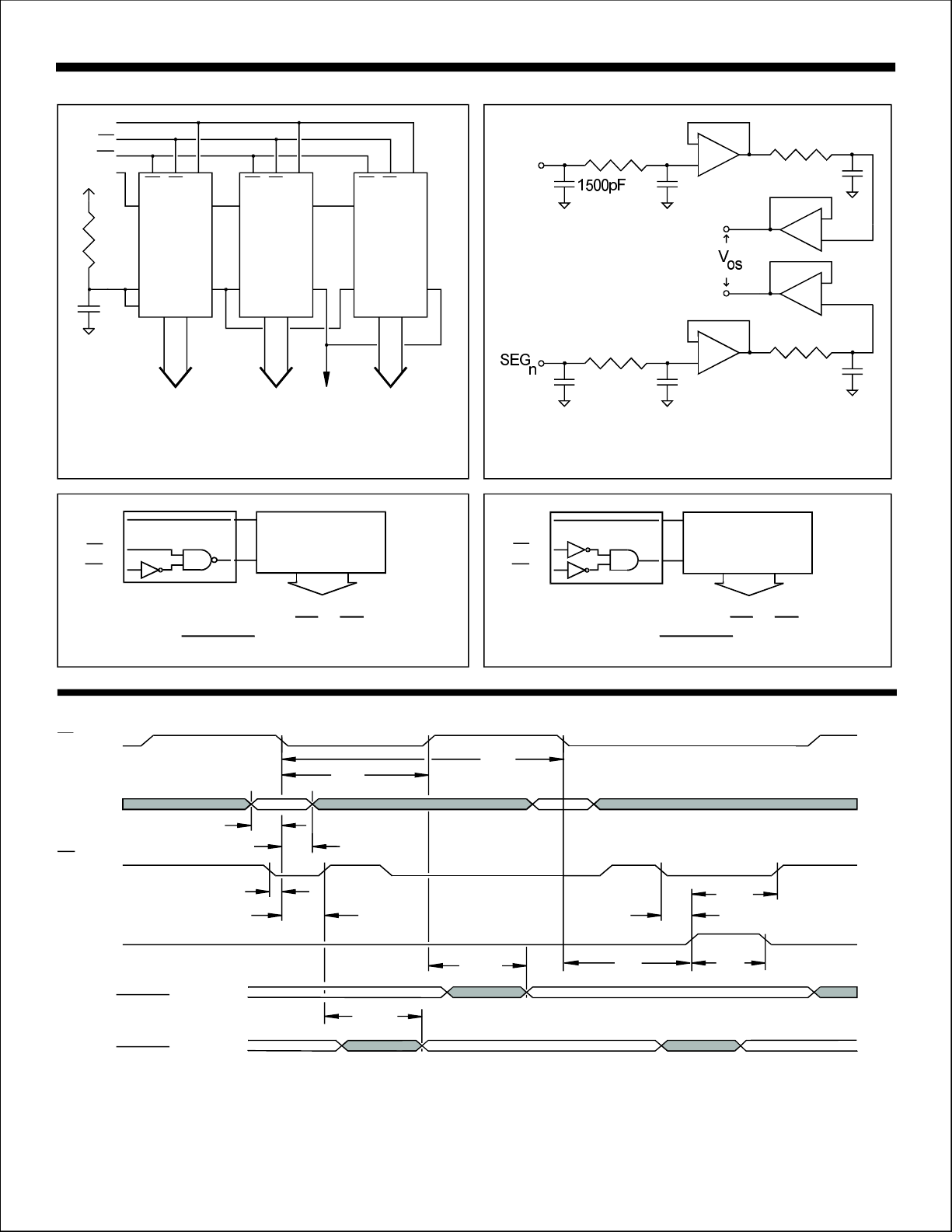
DOUT
TheDOUT30,DOUT32,andDOUT38pinsareavailablefor
cascadingdevicestodrivemoresegments(SeeFigure3)and
forverifyingtheintegrityoftheshiftregisterdata.Theoutputs
candrive2TTLloads.Theychangeonthepositiveedgeof
.CL
AUTOMATICSEGMENTSOFF
Athresholddevicedetectswhenthe5Vsupplyisbelowapproximately1Vandforcesallthesegmentsandthebackplane
tothesamelevel.ThisfeatureisusedtodischargetheVEE
capacitorwhenthe5Vpowerisswitchedoff,toprolongthelife
oftheLCDdisplay.
8020OPT
TheandinputsfunctionthesameastheHI-8010and
CLCS
HI-8110product(SeeFigure5)ifthispinisleftopenorheld
high.Ifheldlow,thetwopinsfunctionthesameastheHI-8020
andHI-8120product(SeeFigure6).Thisinputisavailable
onlyontheHI-8050(TTL)andHI-8150(CMOS)products.
TESTINPUTS
Thetestfunctionsavailableare:
T2T1DisplayodeM
00Normal
01All Off
10AllOn
11AlternatingOn/OffSegments
Thetestinputsmustbetiedtotheappropriatelogiclevelfor
correctcircuitoperation.BothtestinputsareTTLcompatible
ontheHI-8050/51andCMOScompatibleontheHI-8150/51.
V DD
R
BPIN
BPOSC
C
V SS
TOBACKPLANE
TRANSLATOR
ANDDRIVER
Figure1.INTERNALOSCILLATORCIRCUIT
V DD
68K Ω
C
÷256
R
Q
CONVOSC
IN5818,IN5819
CONVOUT
330µH
V SS
VEE
10µF
V SS
Figure2.OPTIONALVOLTAGECONVERTER
HOLTINTEGRATEDCIRCUITS
3
R
OSC
SENSE
Control
V DD
HI-8050/51,HI-8150/51
LD
CL
CS
DIN
R
C
CS
CL LD
DIN
BPOUT
BPIN
BPOSC
SEGMENTS
DO
CS
CL LD
DIN
BPIN
BPOSC
SEGMENTS
DO
BPOUT BPOUT
BACK
PLANE
CS
CL LD
DIN
BPIN
BPOSC
SEGMENTS
Figure3.RCOSCILLATORANDCASCADED
DEVICES
DIN Þ
CL Þ
CS Þ
DATAIN
38Stage
ShiftRegister
CLK
DOUT
Þ
BPOUT
1M Ω
1F µ
DO
1M Ω
360p
1F µ
1M Ω
1F µ
1M Ω
1F µ
Figure4.OFFSETMEASUREMENT
DIN Þ
CL Þ
CS Þ
DATAIN
38Stage
ShiftRegister
CLK
DOUT
Þ
Figure5.HI-8010/HI-8110&LOGIC
(=OPENorHIGH)
8020OPT
CL
INPUT
DIN
INPUT
CS
INPUT
LD
INPUT
DOUT
OUTPUT(floatorhigh)8020OPT
DOUT
OUTPUT(low)8020OPT
t
CSS
t
DS
CLCS
t
DH
t
CSH
t
CW
Figure6.HI-8020/HI-8120&LOGIC
(=LOW)
8020OPT
t
CL
t
CSL
t
CDO
t
CDO
VALID
t
VALID
LS
CLCS
t
LCS
t
LW
VALID
Figure7.TIMINGDIAGRAM
HOLTINTEGRATEDCIRCUITS
4

HI-8050/51,HI-8150/51
ABSOLUTEMAXIMUMRATINGS
VoltagesreferencedtoVSS=0V
SupplyVoltageVDD..........................0Vto7V
VEE................VDD-35Vto0V
Voltageatanyinput,exceptBPIN..-0.3VtoVDD+0.3V
VoltageatBPINinput..............VDD-35VtoVDD+0.3V
DCcurrentperinputpin.....................................10mA
PowerDissipation............................................500mW
NOTE:Stressesabovethoselistedunder"AbsoluteMaximumRatings"maycausepermanentdamagetothedevice.Thesea restressratingsonly.
Functionaloperationofthedeviceattheseoranyotherconditionsabovethoseindicatedintheoperationalsection softhespecificationsisnotimplied.
Exposuretoabsolutemaximumratingconditionsforextendedperiodsmayaffectdevicereliability.
VDD=5V±5%,VEE=-25V,VSS=0V,TA=operatingtemperaturerange(unlessotherwisespecified).
PARAMETERSYMBOLCONDITIONMINTYPMAXUNITS
OperatingVoltageVDD3.07.0V
SupplyCurrent:(ConverterOff,f=0Hz)IDDStatic,NoLoad200µA
BP
InputLowVoltage,HI-8050/51only(exceptBPIN)VILLogicInputs00.8V
InputHighVoltage,HI-8050/51only(exceptBPIN)VIHLogicInputs2VDDV
InputLowVoltage,HI-8150/51only(exceptBPIN)VILLogicInputs00.3VDDV
InputHighVoltage,HI-8150/51only(exceptBPIN)VIHLogicInputs0.7VDDVDDV
InputLowVoltage,BPINVILXVEE0.6VDDV
InputHighVoltage,BPINVIHX0.8VDDVDDV
InputCurrent(exceptT1&T2)IINVIN=0Vto5V100nA
InputCurrent(T1&T2)IINVIN=0Vto5V10
InputCapacitance(Guaranteed,nottested)CI10pF
SegmentOutputImpedanceRSEGIL=10µA1015K
BackplaneOutputImpedanceRBPIL=10µA@25°C450600
Da taOutCurrent:SourceCurrentIDOHVOH=4.5-3.0mA
SinkCurrentIDOLVOL=0.43.2mA
VoltageConverter:@NoLoadVEESeeFig.2-22-21.5-21V
(VDD-VSS=5V,TA=25°C)@0.1mALoadIDDSeeFig.21.8mA
@10KLoadVEESeeFig.2-20V
W
OffsetVoltage(Guaranteed,nottested)VOSSeeFig.425mV
OperatingTemperatureRange(Industrial).......-40°Cto+85°C
(Hi-Temp/Mil).....-55°Cto+125°C
StorageTemperature....................................-65°Cto+125°C
SolderTemperature(Leads).....................+280°Cfor10sec.
(Package)........................................+220°C
JunctionTemperature,Tj..........................................+175°C≤
IEEStatic,NoLoad120µA
TTL
TTL
CMOS
CMOS
1
2
µA
W
W
C
C
HOLTINTEGRATEDCIRCUITS
5

HI-8050/51,HI-8150/51
ACELECTRICALCHARACTERISTICS (SeeFigure7)
VDD=,VEE=-25V,VSS=0V,TA=operatingtemperaturerange(unlessotherwisespecified).5V±5%
PARAMETERSYMBOLVDDMINTYPMAXUNITS
ClockPeriodnon-cascadedt5V250ns
cascadedt5V500ns
ClockPulseWidthnon-cascadedt5V125ns
cascadedt5V250ns
DataIn-Setupt5V80ns
DataIn-Holdt5V80ns
ChipSelect-SetuptoClockt5V100ns
ChipSelect-HoldtoClockt5V120ns
Load-SetuptoClockt5V120ns
ChipSelect-SetuptoLoadt5V0ns
LoadPulseWidtht5V130ns
ChipSelect-HoldtoLoadt5V120ns
DataOutValid,fromClockt5V170ns
CL
CL
CW
CW
DS
DH
CSS
CSH
LS
CSL
LW
LCS
CDO
HI-8051&HI-8151PINCONFIGURATIONS
(Seepage3-27fortheHI-8050&HI-8150pinconfigurations)
LD
DIN
BPIN
BPOSC
VDD
S37
S38
S1
S2
S3
S4
S5
S6
1
2
3
4
5
6
7
8
9
10
11
12
13
HI-8051PQI
HI-8151PQI
HI-8051PQT
&
HI-8151PQT
39
38
37
36
35
34
33
32
31
30
29
28
27
S26
S25
S24
S23
S22
S21
S20
DOUT38
N/C
T2
T1
BPOUT
S19
HOLTINTEGRATEDCIRCUITS
6

ORDERINGINFORMATION
HI-805xPQx
PARTTEMPERATUREBURNLEAD
NUMBERRANGEFLOWINFINISH
PARTPACKAGE
NUMBERDESCRIPTION
PARTLOGIC#
NUMBERINPUTLEVELSSEGMENTS
HI-805TTL38
HI-815CMOS38
HI-8050/51,HI-8150/51
I-40°CTO+85°CINOSOLDER
T-55°CTO+125°CTNOSOLDER
064PINPLASTICTHINFLATQUADPACK(TQFP)
152PINPLASTICQUADFLATPACK(PQFP)
HOLTINTEGRATEDCIRCUITS
7

HI-8050/51,HI-8150/51PACKAGEDIMENSIONS
52PINPLASTICQUADFLATPACK(PQFP)
.520.010±
(13.2 ±.25)
.096MAX.
(2.45MAX.)
SQ.
SeeDetailA
.394 ± .004
(10.00 ± .10)
.079 ± .002
(2.00 ± .05)
SQ.
.010to.020
(0.25to0.50 )
inches(millimeters)
PackageType: 52PQS
.0256BSC
(0.65BSC)
.012 ± .002
(.30 ± .05)
.035+.006/-.004
(.88+.15/-.10)
YP.012RT.
Y(0.30RTP.)
0 °≤Θ≤ 7 °
.008RTYP.
(0.20RTYP.)
ETAILDA
64PINPLASTICTHINQUADFLATPACK(TQFP)
.354.008±
(9.00 ±.20)
.063MAX.
(1.60MAX. )
SQ.
.276.004±
(7.00 ± .10)
SeeDetailA
SQ.
.055.002±
(1.4 ± .05)
(0.10 ±).05
.008RTYP.
(0.20RTYP. ).004.002±
PackageType: 64PTQS
PackageType:
.0157BSC
(0.40BSC )
.007.004±
(0.18 ±).05
.024+.006/-.004
(0.60+.15/-.10 )
.008RTYP.
(0.20RTYP. )
0°7°≤Θ≤
DetailA
HOLTINTEGRATEDCIRCUITS
8
 Loading...