

Page 1
TM
www.BDTIC.com/Intersil
HI-574A, HI-674A
itle
I4A,
4A,
-
4)
bjec
omp
e,
-Bit
D
nver
s
th
crop
esso
erfa
utho
)
eyw
s
tersi
rpor
on,
ico
ucto
/D,
C,
sh,
nver
, bit,
le
dem
Data Sh eet June 200 1
Complete, 12-Bit A/D Converters with
Microprocessor Interface
The HI-X74(A) is a complete 12-bit, Analog-to-Digital
Converter, including a +10V reference clock, three-state
outputsand a digital i nterface for microprocessor control.
Successive approximation conversion is performed by two
monolithic dice housed in a 28 lead package. The bipolar
analog die features the Intersil Dielectric Isolation process,
which provides enhanced AC performance and freedom
from latch-up.
Custom design of each IC (bipolar analog and CMOS digital)
has yielded improved performance over existing versions of
this converter. The voltage comparatorfeatures high PSRR
plus a high speed current-mode latch, and provides precise
decisionsdown t o 0.1 LSB of input overdrive. More than 2X
reduction in noise has been achieved by using current
insteadof voltage for transmission of all signals between the
analog and digital ICs. Also, the clock oscillator is current
controlled for excellent stability over temperature.
The HI-X74(A) offers standard unipolar and bipolar input
ranges, laser trimmed for specified linearity,gain and offset
accuracy. The low noise buried zener reference c ircuit is
trimmed for minimum temperature coefficient.
Power requirements are +5V and ±12V to ±15V, with typical
dissipation of 385mW (HI-574A/674A) at 12V.
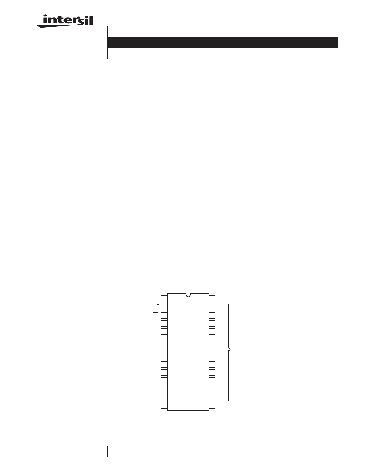
Pinout
+5V SUPPLY, V
DA TAMODE SEL, 12/8
CHIP SEL, CS
BYTEADDR/SHORT
CYCLE,A
READ/CONVERT, R/C
CHIP ENABLE, CE
+12V/+15V SUPPLY, V
+10VREF,REF OUT
ANALOG
COMMON,AC
REFERENCEINPUT
-12V/-15V SUPPLY, V
BIPOLAR OFFSET
BIP OFF
10V INPUT
20V INPUT
LOGIC
CC
EE
1
2
3
4
O
5
6
7
8
9
10
11
12
13
14
(PDIP, SBDIP)
TOP VIEW
File Number 3096.5
Features
• Complete 12-Bit A/D Converter with Reference and Clock
• Full 8-Bit, 12-Bit or 16-Bit Microprocessor Bus Interface
• BusAccessTime...........................150ns
• No Missing Codes Over Temperature
• Minimal Setup Time for Control Signals
• Fast Conversion Times
- HI-574A(Max) ............................25µs
- HI-674A(Max) ............................15µs
• Low Noise, via Current-Mode Signal Transmission
Between Chips
• Byte Enable/Short Cycle (A
O
Input)
- Guaranteed Break-Before-Make Action, Eliminating Bus
Contention During Read Operation. Latched by Start
Convert Input (T oSet the Conversion Length)
• Supply Voltage. ..................... ±12V to ±15V
Applications
• Military and Industrial Data Acquisition Systems
• Electronic Testand Scientific Instrumentation
• Process Control Systems
28
STATUS, STS
27
DB11
MSB
26
DB10
25
DB9
24
DB8
23
DB7
22
21
20
19
18
17
16
15
DIGITAL
DATA
DB6
OUTPUTS
DB5
DB4
DB3
DB2
DB1
DB0
LSB
DIG COMMON,
DC
1
1-888-INTERSIL or 321-724-7143
CAUTION: These devices aresensitiveto electrostatic discharge;followproperIC Handling Procedures.
| Intersil and Design is a trademark of IntersilAmericasInc. | Copyright © Intersil Americas Inc. 2001
Page 2
HI-574A, HI-674A
www.BDTIC.com/Intersil
Ordering Information
PART NUMBER INL
HI3-574AJN-5 ±1.0LSB 0to75 28LdPDIP E28.6
HI3-574AKN-5 ±0.5LSB 0to75 28LdPDIP E28.6
HI1-574AJD-5 ±1.0LSB 0to75 28LdSBDIP D28.6
HI1-574AKD-5 ±0.5LSB 0to75 28LdSBDIP D28.6
HI1-574ASD-2 ±1.0LSB -55to125 28LdSBDIP D28.6
HI1-574ATD-2 ±0.5LSB -55to125 28LdSBDIP D28.6
HI1-574ASD/883 ±1.0LSB -55to125 28LdSBDIP D28.6
HI1-574ATD/883 ±0.5LSB -55to125 28LdSBDIP D28.6
HI3-674AJN-5 ±1.0LSB 0to75 28LdPDIP E28.6
HI3-674AKN-5 ±0.5LSB 0to75 28LdPDIP E28.6
HI1-674AJD-5 ±1.0LSB 0to75 28LdSBDIP D28.6
HI1-674AKD-5 ±0.5LSB 0to75 28LdSBDIP D28.6
HI1-674ASD-2 ±1.0LSB -55to125 28LdSBDIP D28.6
HI1-674ATD/883 ±0.5LSB -55to125 28LdSBDIP D28.6
TEMPERATURE RANGE
(oC) PACKAGE PKG. NO.
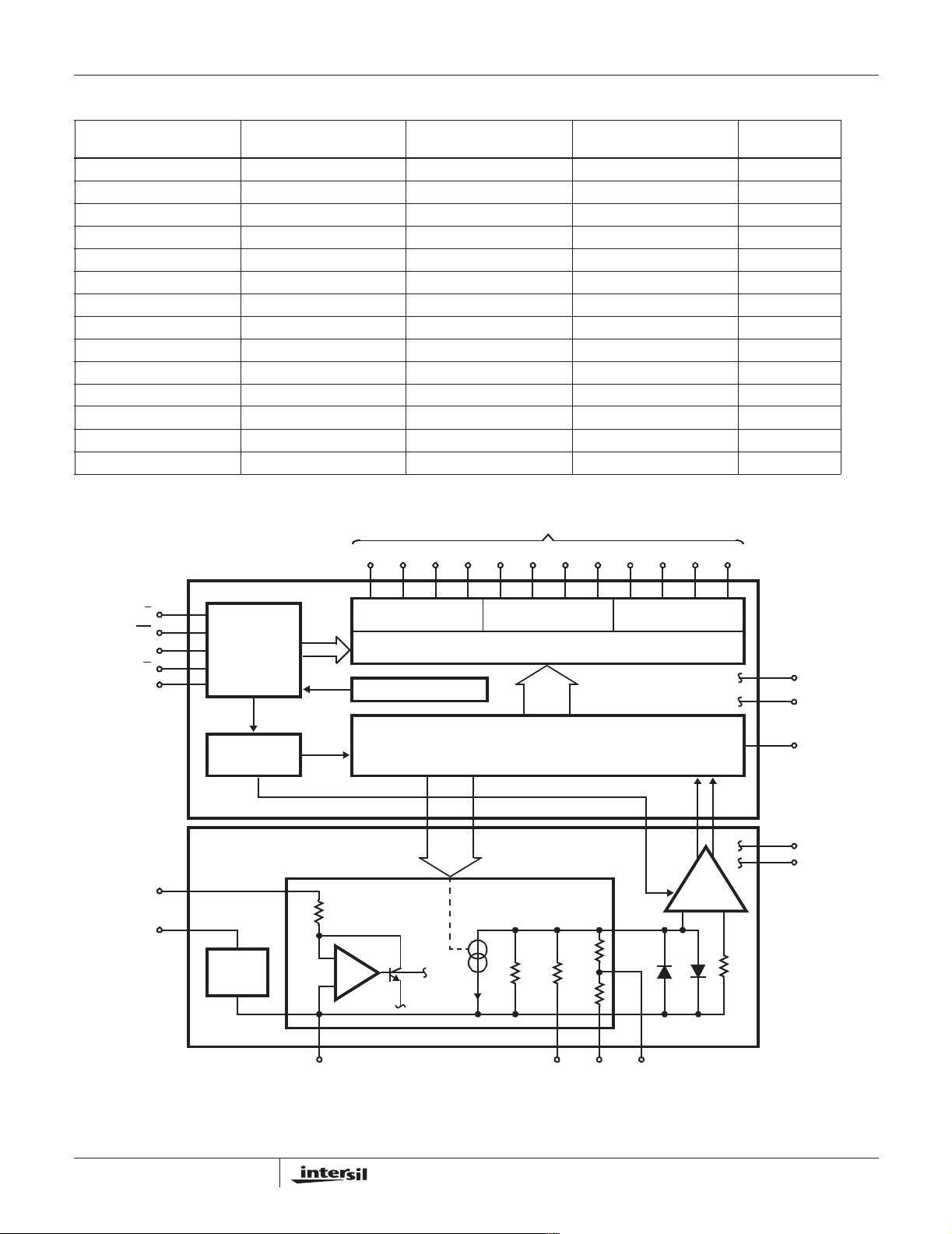
Functional Block Diagram
BIT OUTPUTS
MSB LSB
12/8
CS
A
O
R/C
CE
IN
V
REF
V
OUT
REF
CONTROL
LOGIC
OSCILLATOR
DIGITAL CHIP
ANALOG CHIP
+10V
REF
THREE-STATE BUFFERS AND CONTROL
POWER-UP RESET
CLK
12 BITS
10K
+
-
5K
NIBBLE B (NOTE) NIBBLE C (NOTE)NIBBLE A (NOTE)
12 BITS
SAR
DAC
10K
STROBE
5K
5K
-
COMP
+
2.5K
V
LOGIC
DIGITAL
COMMON
STS
V
CC
V
EE
ANALOG
COMMON
BIP
OFF
INPUT
INPUT
10V
20V
NOTE: “Nibble”is a 4-bit digital w ord.
2
Page 3
HI-574A, HI-674A
www.BDTIC.com/Intersil
Absolute M axi m um Rati ng s Thermal Information
Supply Voltage
toDigitalCommon......................0Vto+16.5V
V
CC
toDigitalCommon.......................0Vto-16.5V
V
EE
V
toDigitalCommon ......................0Vto+7V
LOGIC
Analog Common to Digital Common. . . . . . . . . . . . . . . . . . . . . . ±1V
Control Inputs
Analog Inputs
REFOUT.....Indefinite Short ToCommon, Momentary Short To V
,AO,12/8,R/C) to Digital Common . . -0.5V to V
(CE, CS
(REFIN,BIPOFF,10VIN)toAnalogCommon..........±16.5V
20VINtoAnalogCommon..........................± 24V
LOGIC
+0.5V
CC
Operating Conditions
TemperatureRange
HI3-574Axx-5,HI1-674Axx-5...................0
HI1-574AxD-2,HI1-674AxD-2............... -55
CAUTION: Stresses above those listed in “Absolute Maximum Ratings” may cause permanent damage to the device. This is a stress only rating and operationofthe
device at these or any other conditions above those indicated in the operational sections of this specification is not implied.
NOTE:
1. θ
is measured with the component mountedon a low effectivethermalconductivity test boardin free air. See Tech B rief TB379 for details.
JA
o
Cto75oC
o
Cto125oC
Thermal Resistance (Typical, Note 1) θ
SBDIPPackage.................. 55 18
PDIPPackage................... 60 N/A
Maximum JunctionTemperature
PDIPPackage...................................150
SBDIPPackage..................................175
Maximum Storage TemperatureRange
PDIPPackage.............................-40
SBDIPPackage...........................-65
MaximumLeadTemperature(Soldering,10s)............300
(oC/W) θJC(oC/W)
JA
o
Cto85oC
o
Cto150oC
Die Characteristics
TransistorCount
HI-574A,HI-674A..................................1117
o
C
o
C
o
C
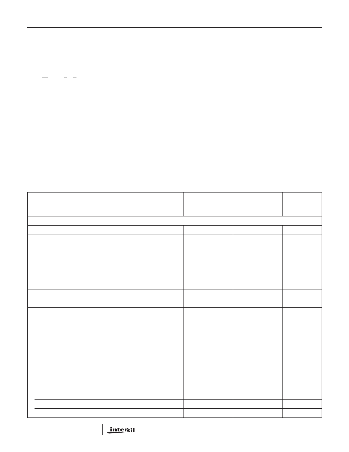
DC and Transfer Accuracy Specifications Typical at 25
UnlessOtherwise Specified
PARAMETER
DYNAMIC CHARACTERISTICS
Resolution (Max) 12 12 Bits
Linearity Error
o
25
C(Max) ±1 ±1/
o
0
Cto75oC(Max) ±1 ±1/
Max Resolution For Which No Missing Codes Is Guaranteed
o
25
C 12 12 Bits
T
to T
MIN
MAX
Unipolar Offset (Max)
Adjustable to Zero ±2 ±1.5 LSB
Bipolar Offset (Max)
V
= 0V (Adjustable to Zero) ±4 ±4LSB
IN
VIN=-10V ±0.15 ±0.1 % of FS
Full Scale Calibration Error
o
25
C (Max), With Fixed 50Ω Resistor From REF OUT To REF IN
(Adjustableto Zero)
to T
T
MIN
T
to T
MIN
Temperature Coefficients
Guaranteed Max Change, T
Unipolar Offset ±2 ±1LSB
Bipolar Offset ±2 ±1LSB
Full Scale Calibration ±9 ±2LSB
(No Adjustment At 25oC) ±0.475 ±0.375 %of FS
MAX
(WithAdjustment To Zero 25oC) ±0.22 ±0.12 % of FS
MAX
MIN
to T
(Using Internal Reference)
MAX
o
CwithVCC= +15V or +12V, V
TEMPERATURE RANGE
-5 (0
11 12 Bits
±0.25 ±0.25 % of FS
LOGIC
o
Cto75oC)
=+5V,VEE=-15Vor-12V,
UNITSJ SUFFIX K SUFFIX
2
2
LSB
LSB
3
Page 4
HI-574A, HI-674A
www.BDTIC.com/Intersil
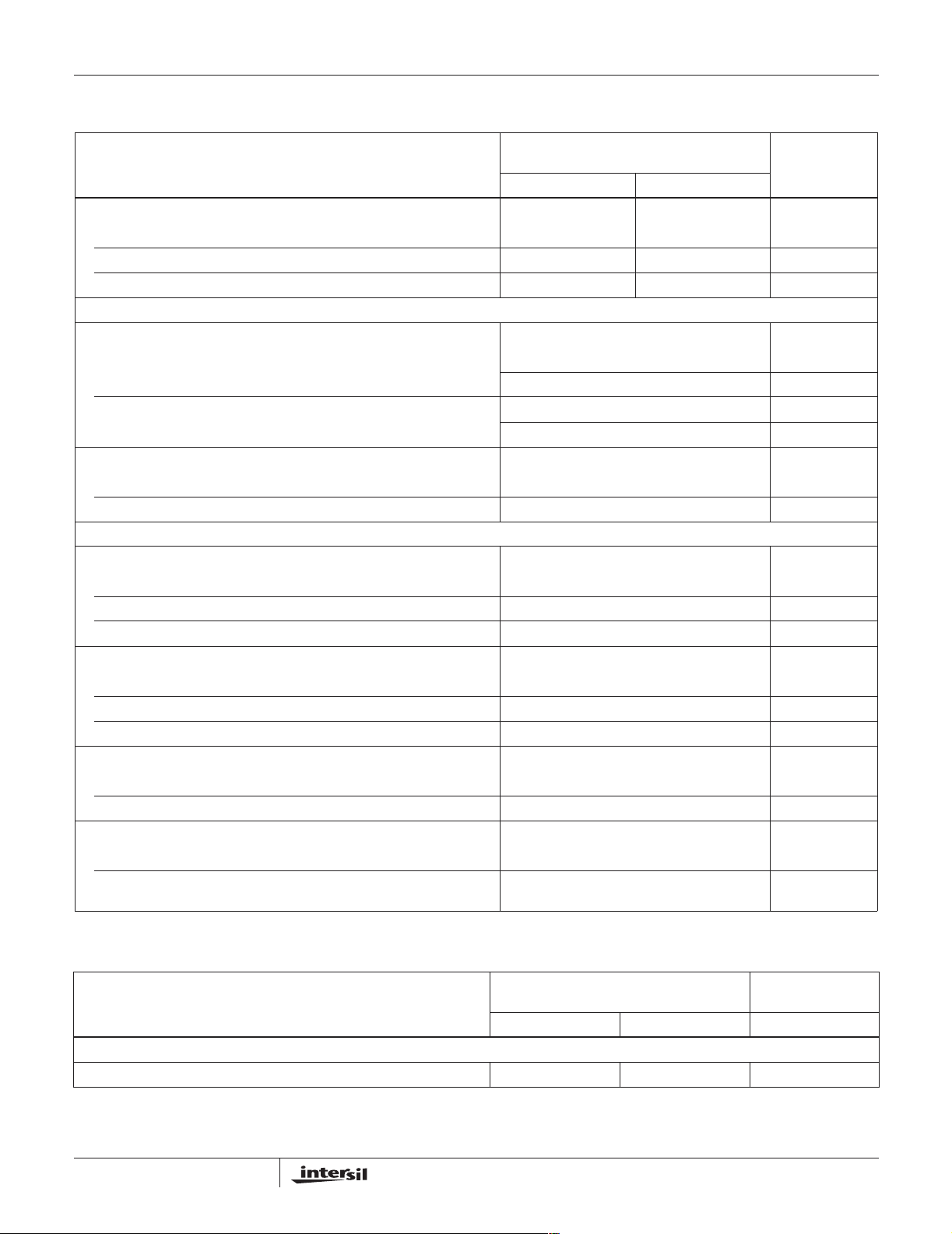
DC and Transfer Accuracy Specifications Typical at 25
UnlessOtherwise Specified (Continued)
PARAMETER
Power Supply Rejection Max Change In Full ScaleCalibration
+13.5V < V
+4.5V < V
-16.5V< VEE< -13.5Vor -12.6V < VEE<-11.4V ±2 ±1LSB
ANALOG INPUTS
Input Ranges
Bipolar -5 to +5 (Note 3) V
Unipolar 0to+10(Note3) V
Input Impedance
10V Span 5K, ±25% Ω
20V Span 10K, ±25% Ω
POWER SUPPLIES
Operating Voltage Range
V
LOGIC
V
CC
V
EE
Operating Current
I
LOGIC
I
+15V Supply 11 Typ, 15 Max mA
CC
IEE-15V Supply 21 Typ, 28 Max mA
Power Dissipation
±15V, +5V 515 Typ, 720 Max mW
±12V, +5V 385 Typ mW
Internal Reference Voltage
T
to T
MIN
Output Current, Available For External Loads (External Load Should Not
Change During Conversion).
< +16.5V or +11.4V < VCC<+12.6V ±2 ±1LSB
CC
<+5.5V ±1/
LOGIC
MAX
o
CwithVCC= +15V or +12V, V
TEMPERATURE RANGE
-5 (0
2
-10 to +10 (Note 4) V
0to+20(Note4) V
+4.5to +5.5 V
+11.4to+16.5 V
-11.4to-16.5 V
7Typ,15Max mA
+10.00 ±0.05 Max V
=+5V,VEE=-15Vor-12V,
LOGIC
o
Cto75oC)
UNITSJ SUFFIX K SUFFIX
±1/
2
2.0 Max mA
LSB
8
DC and Transfer Accuracy SpecificationsTypical at 25
UnlessOtherwise Specified (Continued)
PARAMETER
DYNAMIC CHARACTERISTICS
Resolution (Max) 12 12 Bits
o
CwithVCC= +15V or +12V, V
TEMPERATURE RANGE
-2 (-55
S SUFFIX T SUFFIX UNITS
LOGIC
o
Cto125oC)
=+5V,VEE=-15Vor-12V,
4
Page 5
HI-574A, HI-674A
www.BDTIC.com/Intersil
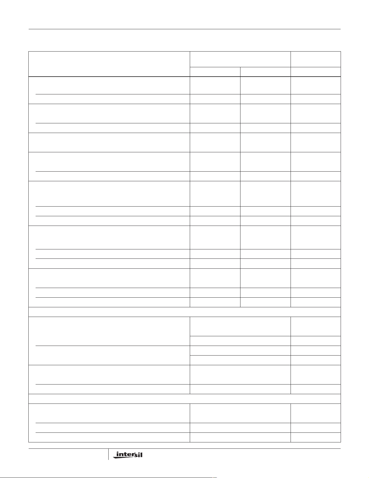
DC and Transfer Accuracy SpecificationsTypical at 25
UnlessOtherwise Specified (Continued)
PARAMETER
Linearity Error
o
25
C ±1 ±1/
o
-55
Cto125oC(Max) ±1 ±1LSB
Max ResolutionFor Which No Missing Codes Is Guaranteed
o
25
C 12 12 Bits
T
to T
MIN
MAX
Unipolar Offset ( Max)
Adjustable to Zero ±2 ±1.5 LSB
Bipolar Offset (Max)
V
= 0V (Adjustable to Zero) ±4 ±4LSB
IN
=-10V ±0.15 ±0.1 % of FS
V
IN
Full Scale Calibration Error
o
25
C(Max),WithFixed50Ω Resistor From REF OUT To REF IN
(Adjustable To Zero)
to T
T
MIN
T
to T
MIN
Temperature Coefficients
Guaranteed Max Change,T
Unipolar Offset ±2 ±1LSB
Bipolar Offset ±2 ±2LSB
Full Scale Calibration ±20 ±10 LSB
Power Supply RejectionMax Change In Full Scale Calibration
+13.5V< V
+4.5V< V
-16.5V < V
ANALOG INPUTS
InputRanges
Bipolar -5 to +5 (Note 3) V
Unipolar 0to+10(Note3) V
Input Impedance
10V Span 5K, ±25% Ω
20V Span 10K, ±25% Ω
POWER SUPPLIES
Operating Voltage Range
V
LOGIC
V
CC
V
EE
(No Adjustment At 25oC) ±0.75 ±0.50 % of FS
MAX
(With Adjustment To Zero At 25oC) ±0.50 ±0.25 % of FS
MAX
to T
MIN
< +16.5V or +11.4V < VCC<+12.6V ±2 ±1LSB
CC
< +5.5V ±1/
LOGIC
< -13.5V or -12.6V < VEE<-11.4V ±2 ±1LSB
EE
(Using Internal Reference)
MAX
o
CwithVCC= +15V or +12V, V
TEMPERATURE RANGE
-2 (-55
S SUFFIX T SUFFIX UNITS
11 12 Bits
±0.25 ±0.25 % of FS
2
-10to+10(Note4) V
0to+20(Note4) V
+4.5 to +5.5 V
+11.4to+16.5 V
-11.4to-16.5 V
LOGIC
o
Cto125oC)
=+5V,VEE=-15Vor-12V,
2
±1/
2
LSB
LSB
5
Page 6
HI-574A, HI-674A
www.BDTIC.com/Intersil
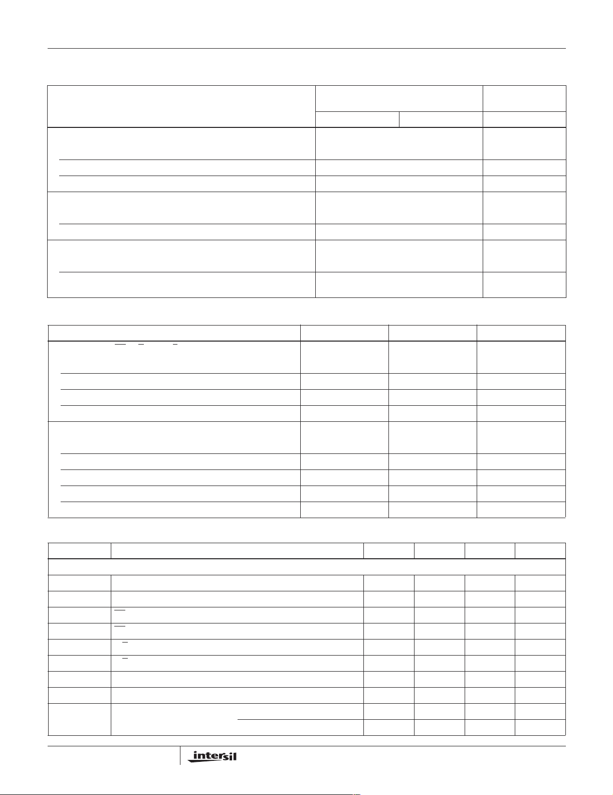
DC and Transfer Accuracy SpecificationsTypical at 25
UnlessOtherwise Specified (Continued)
PARAMETER
Operating Current
I
LOGIC
I
+15V Supply 11 Typ, 15 Max mA
CC
IEE-15V Supply 21 Typ, 28 Max mA
Power Dissipation
±15V, +5V 515 Typ, 720 Max mW
±12V, +5V 385 Typ mW
Internal Reference Voltage
T
to T
MIN
MAX
Output current, available for external loads (external load should not
change duringconversion).
o
CwithVCC= +15V or +12V, V
TEMPERATURE RANGE
-2 (-55
S SUFFIX T SUFFIX UNITS
7Typ,15Max mA
+10.00±0.05 Max V
=+5V,VEE=-15Vor-12V,
LOGIC
o
Cto125oC)
2.0 Max mA
Digital Specifications All Models, Over Full T emperature Range
PARAMETER MIN TYP MAX
LogicInputs (CE, CS
Logic “1” +2.4V - +5.5V
Logic “0” -0.5V - +0.8V
Current - ±0.1µA ±5µA
Capacitance - 5pF -
LogicOutputs(DB11-DB0, STS)
Logic “0” (I
Logic “1” (I
Logic “1” (I
Leakage (High-Z State, DB11-DB0 Only) - ±0.1µA ±5µA
Capacitance - 5pF -
,R/C,AO,12/8)
- 1.6mA) - - +0.4V
SINK
SOURCE
SOURCE
-500µA) +2.4V - -
-10µA) +4.5V - -
Timing Specification s (HI-574A)25
SYMBOL PARAMETER MIN TYP MAX UNITS
CONVERT MODE
t
DSC
t
HEC
t
SSC
t
HSC
t
SRC
t
HRC
t
SAC
t
HAC
t
C
STS Delay from CE - - 200 ns
CE Pulse Width 50 - - ns
CSto CE Setup 50 - - ns
CSLow During CE High 50 - - ns
R/Cto CE Setup 50 - - ns
R/CLow During CE High 50 - - ns
AOto CE Setup 0 - - ns
AOValidDuringCEHigh 50 - - ns
Conversion T ime 12-Bit Cycle T
o
C, Note 2, Unless Other wise Specified
to T
MIN
MAX
8-Bit Cycle T
MIN
to T
MAX
15 20 25 µs
10 13 17 µs
6
Page 7
HI-574A, HI-674A
www.BDTIC.com/Intersil
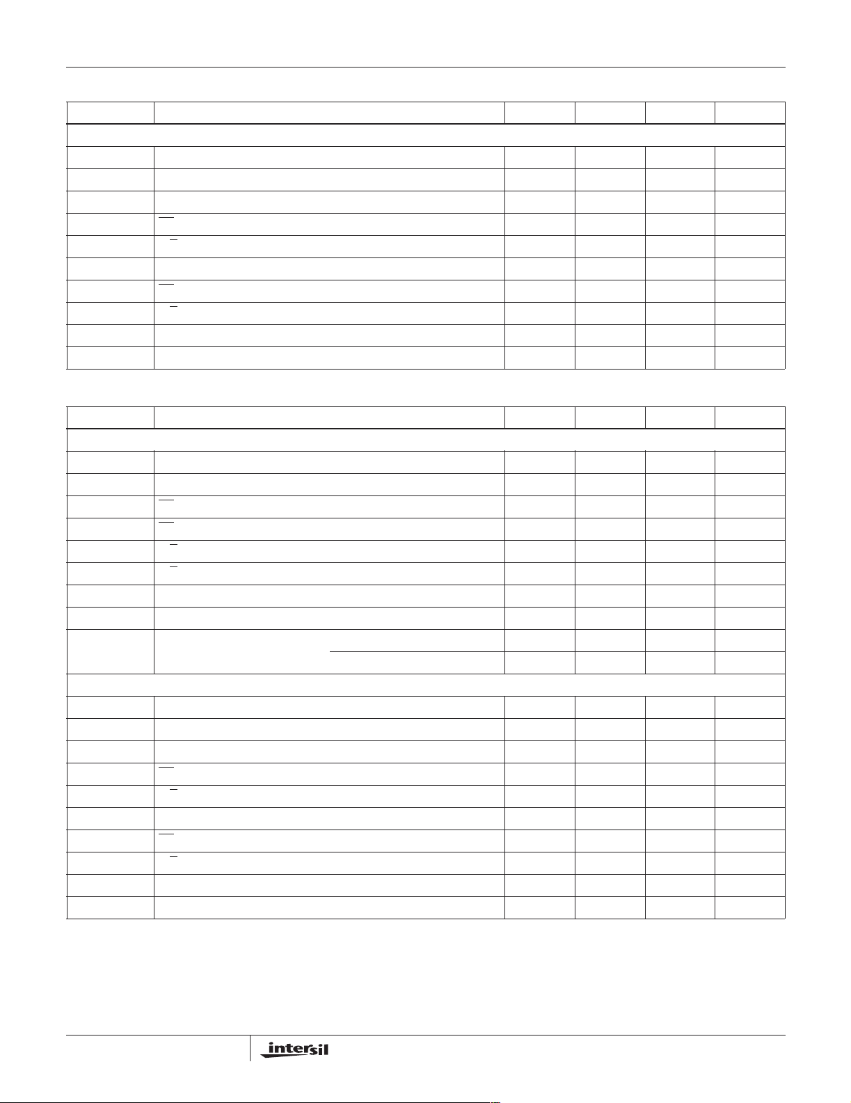
Timing Specification s (HI-574A)25
SYMBOL PARAMETER MIN TYP MAX UNITS
READ MODE
t
DD
t
HD
t
t
SSR
t
SRR
t
SAR
t
HSR
t
HRR
t
HAR
t
HS
HL
Access Time from CE - 75 150 ns
Data Valid After CE Low 25 - - ns
Output Float Delay - 100 150 ns
CSto CE Setup 50 - - ns
R/Cto CE Setup 0 - - ns
AOto CE Setup 50 - - ns
CSValid After CE Low 0 - - ns
R/CHigh After CE Low 0 - - ns
AOValid After CE Low 50 - - ns
STS Delay After Data Valid 300 - 1200 ns
Timing Specification s (HI-674A)25
SYMBOL PARAMETER MIN TYP MAX UNITS
CONVERT MODE
t
DSC
t
HEC
t
SSC
t
HSC
t
SRC
t
HRC
t
SAC
t
HAC
t
C
READ MODE
t
DD
t
HD
t
HL
t
SSR
t
SRR
t
SAR
t
HSR
t
HRR
t
HAR
t
HS
NOTES:
2. Time is measured from 50% level of digital transitions. Tested with a 50pF and 3kΩ load.
3. For the “10V Input”, Pin 13.
4. For the “20V Input”, Pin 14.
STS Delay from CE - - 200 ns
CE Pulse Width 50 - - ns
CSto CE Setup 50 - - ns
CSLow During CE High 50 - - ns
R/Cto CE Setup 50 - - ns
R/CLow During CE High 50 - - ns
AOto CE Setup 0 - - ns
AOValidDuringCEHigh 50 - - ns
Conversion T ime 12-Bit Cycle T
Access Time from CE - 75 150 ns
Data Valid After CE Low 25 - - ns
Output Float Delay - 100 150 ns
CSto CE Setup 50 - - ns
R/Cto CE Setup 0 - - ns
AOto CE Setup 50 - - ns
CSValid After CE Low 0 - - ns
R/CHigh After CE Low 0 - - ns
AOValid After CE Low 50 - - ns
STS Delay After Data Valid 25 - 850 ns
o
C, Note 2, Unless Other wise Specified (Continued)
o
C, Note 2, Unless Other wise Specified
to T
MIN
MAX
8-Bit Cycle T
MIN
to T
MAX
91215µs
6810µs
7
Page 8
HI-574A, HI-674A
www.BDTIC.com/Intersil
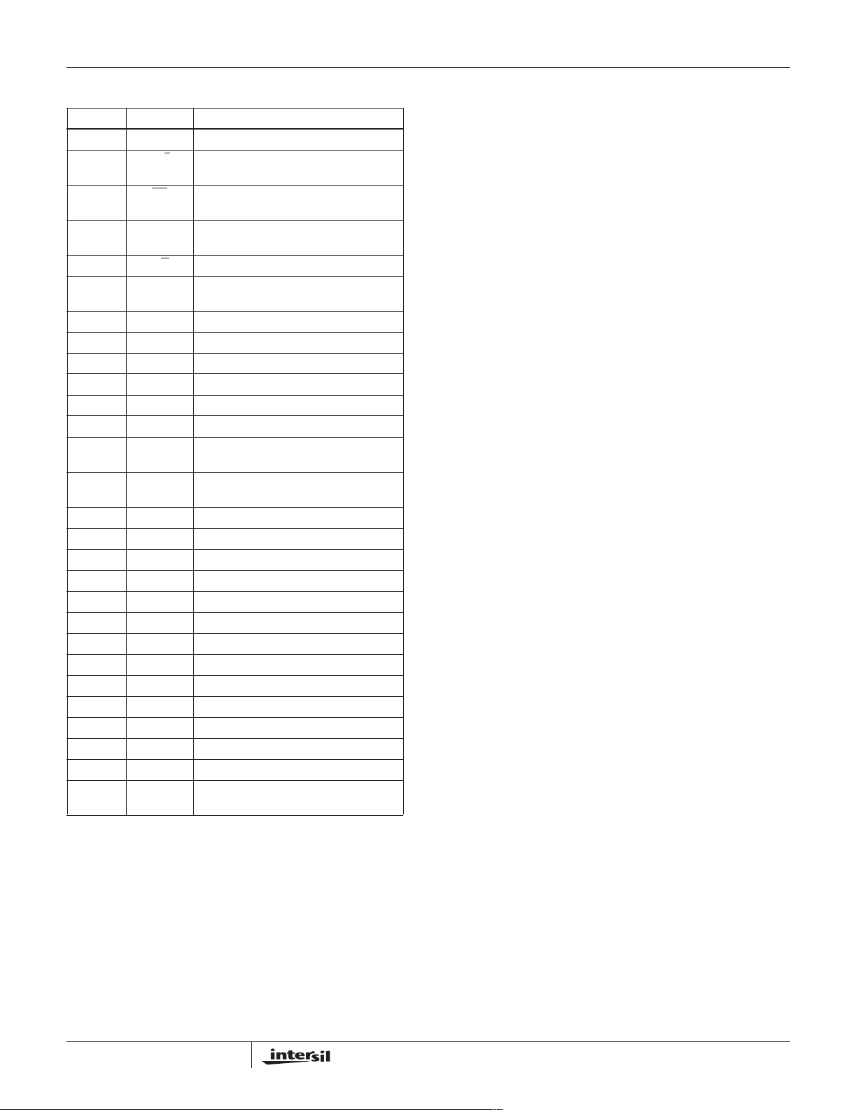
Pin Descriptions
PIN SYMBOL DESCRIPTION
1V
212/8
3CS
4A
5R/C
6 CE Chip Enable - Chip Enable low disables
7V
8 REF OUT +10V Reference
9 AC Analog Common
10 REF IN Reference Input
11 V
12 BIP OFF Bipolar Offset
13 10V Input 10V Input - Used for 0V to 10V and -5V to
14 20V Input 20V Input - Used for 0V to 20Vand -10V to
15 DC Digital Common
16 DB0 DataBit0(LSB)
17 DB1 Data Bit 1
18 DB2 Data Bit 2
19 DB3 Data Bit 3
20 DB4 Data Bit 4
21 DB5 Data Bit 5
22 DB6 Data Bit 6
23 DB7 Data Bit 7
24 DB8 Data Bit 8
25 DB9 Data Bit 9
26 DB10 Data Bit 10
27 DB11 Data Bit 11 (MSB)
28 STS StatusBit - Statushigh implies a conversion
LOGIC
Logic supply pin (+5V)
Data Mode Select - Selects between 12-
bit and 8-bitoutput modes.
Chip Select - Chip Select high disables
the device.
Byte Address/Short Cycle - See Table 1
O
for operation.
Read/Convert - See Table 1 for operation.
the device.
Positive Supply (+12V/+15V)
CC
Negative Supply (-12V/-15V).
EE
+5V input ranges.
+10V input ranges.
is in progress.
Definitions of Specifications
Linearity Error
Linearity error refers to the deviation of each individual code
from a line drawn from “zero” through “full scale”. The point
used as “zero” occurs
the first code transition (all zeros to only the LSB “on”). “Full
scale” is defined as a level 1
transition (to all ones). The deviation of a code from the true
straight line is measured from the middle of each particular
code.
1
/2LSB (1.22mV for 10V span) before
1
/2LSB beyond the last code
The HI-X74AK grade is guaranteed for maximum nonlinearity
1
of ±
/2LSB. For this grade, this means that an analog value
which falls exactly in the center of a given code width will result
in the correct digital output code. V aluesnearer the upper or
lower transition of the code width may produce the next upper
or lower digital output code. The HI-X74AJ is guaranteed to ±1
LSB max error. For this grade, an analog value which falls
within a given code width will result in either the correct code for
that region or either adjacent one.
Note that the linearity error is not user-adjustable.
Differential Linearity Error (No Missing Codes )
A specification which guarantees no missing codes requires
that every code combination appear in a monotonic
increasing sequence as the analog input level is increased.
Thus every code must have a finite width. For the HI-X74AK
grade, which guarantees no missing codes to 12-bit
resolution, all 4096 codes must be present over the entire
operating temperature ranges. The HI-X74AJ grade
guarantees no missing codes to 11-bit resolution over
temperature; this means that all code combinations of the
upper 1 1 bits must be present; in practice very few of the 12bit codes are missing.
Unipolar O ffset
The first transition should occur at a level1/2LSB above analog
common. Unipolar offset is defined as the deviation of the
actual transition from that point. This offset can be adjusted as
discussed on the following pages. The unipolar offset
temperature coefficient specifies the maximum change of the
transition point over temperature, with or without external
adjustment.
Bipolar Offset
Similarly, in the bipolar mode, the major carry transition
(0111 1111 1111 to 1000 0000 0000) should occur for an
analog value
1
/2LSB below analog common. The bipolar
offset error and temperature coefficient specify the initial
deviation and maximum change in the error over
temperature.
Full Scale Calibration Error
The last transition (from 1111 1111 1110 to 1111 1111
1111) should occur for an analog value 1
nominal f ull scale (9.9963V for 10.000V full scale). The full
scale calibration error is the deviation of the actual level at
the last transition f rom the ideal level. This error,which is
typically0.05 to 0. 1% of full scale, can be trimmed out as
shown in Figures 2 and 3. The full scale calibration error
over temperature is given with and without the initial error
trimmed out. The temperature coefficients for each grade
indicate the maximum change in the full scale gain from the
initial value using the internal 10V reference.
1
/2LSB below the
Temperature Coefficients
The temperature c oefficients for full-scale calibration,
unipolar offset, and bipolar offset specify the maximum
8
Page 9

HI-574A, HI-674A
www.BDTIC.com/Intersil
change from the initial (25oC)valuetothevalueatT
T
.
MAX
MIN
or
Power Supply Rejection
The standard specifications for the HI-X74A assume use of
+5.00V and ±15.00V or ±12.00V supplies. The only effect of
power supply error on the performance of the device will be
a small change in the full scale calibration. This will result in
a linear change in all lower order codes. The specifications
show the maximum change in calibration from the initial
value with the supplies at the various limits.
Code Width
A fundamental quantity for A/D converter specifications is
the code width. This is defined as the range of analog input
values f or which a given digital output code will occur.The
nominal value of a code width is equivalent to 1 least
significant bit (LSB) of the full scale range or 2.44mV out of
10V for a 12-bit ADC.
Quantization Uncertainty
Analog-to-digital c onverters exhibit an inherent quantization
uncertainty of ±
characteristic of the quantization process and cannot be
reduced for a converter of given resolution.
1
/2LSB. This uncertainty is a fundamental
Left-Justified Data
The data format used in the HI-X74A is left-justified. This
means that the data represents the analog input as a
fraction of full-scale, ranging from 0 to . This implies a
binary point to the left of the MSB.
4095
4096
Power Supplies
Supply voltages to the HI-X74A (+15V,-15V and +5V) must be
“quiet” and well regulated. Voltage spikes on these lines can
affect the converter’s accuracy, causing several LSBs to flicker
when a constant input is applied. Digital noise and spikes from
a switching power supply are especially troublesome. If
switching supplies must be used, outputs should be carefully
filtered to assure “quiet” DC voltage at the converter terminals.
Further, a bypass capacitor pair on each supply voltage
terminal is necessary to counter the effect of variations in
supply current. Connect one pair from pin 1 to 15 ( V
supply),one f rom pin 7 to 9 (VCCto Analog Common) and
onefrompin11to9(V
capacitorpair,a 10µF tantalum type in parallel with a 0.1µF
ceramic type is recommended.
to Analog Common). For each
EE
LOGIC
Ground Connections
Pins9 and 15 shouldbe tied togetherat the packageto
guarantee specifiedperformancefor the converter. In
addition, a wide PC trace should run directly from pin 9 to
(usually)+15V common, and frompin 15 to (usually)the +5V
Logic Common. If the converter is located some distance from
the system’s “single point”ground,make only these
connections to pins9 and 15: Tiethem together at the
package, and back to the system ground with a single path.
This path should have low resistance. (Code dependent
currents flow in the V
through the HI-X74A’s Analog Common or Digital Common).
CC,VEE
and V
terminals,but not
LOGIC
Analog Signal Source
Applying the HI-X74A
For each application of this converter, the ground
connections,power supply bypassing, analog signalsource,
digitaltiming and signal routing on the circuit board must be
optimizedto assure maximum performance. These areas
are reviewed in the following sections, along with basic
operatingmodes and calibration requirements.
Physical Mounting and Layout Considerations
LAYOUT
Unwanted, parasitic circuit components, (L, R, and C) can
make 12-bit accuracy impossible,even with a perfect A/D
converter. The best policy is to eliminate or minimize these
parasitics through proper circuit layout, rather than t ry to
quantify their effects.
The recommended construction is a double-sided printed
circuit boardwith a groundplaneon the component side.
Other techniques,such as wire-wrapping or point-to-point
wiring on vector board, will have an unpredictable effect on
accuracy.
In general, sensitive analog signals should be routed between
groundtraces and kept well away fromdigitallines.If analog
and digital lines must cross, they should do so at right angles.
HI-574A a nd HI-674A
The device chosen to drive the HI-X74A analog input will see a
nominal load of 5kΩ (10V range) or 10kΩ (20V range).
However, the other end of these input resistors may change
±400mV with each bit decision, creating abrupt changes in
current at the analog input. Thus, the signal source must
maintain its output voltage while furnishing these step changes
in load current, which occur at 1.6µs and 950ns intervals for the
HI-574A and HI-674A, respectively .This requires low output
impedance and fast settling by the signal source.
The output impedance of an op amp, for example, has an
open loop value which, in a closed loop, is divided by the
loop gain available at a frequency of interest. The amplifier
should have acceptable loop gain at 600kHz for use with the
HI-X74A. To check whether the output properties of a signal
source are suitable,monitor the HI-X74A’s input (pin 13 or
14) with an oscilloscope while a conversion is in progress.
Each of the twelve disturbances should subside in 1µsor
less for the HI-574A and 500ns or less for the HI-674A. (The
comparatordecision is made about 1.5µs and 850ns after
each code change from the SAR f or the HI-574A and
HI-674A, respectively.)
If the application calls for a Sample/Hold to precede the
converter, it should be noted that not all Sample/Holds are
compatiblewith the HI-574A in the manner described above.
9
Page 10
HI-574A, HI-674A
www.BDTIC.com/Intersil
These will require an additional wi deband buffer amplifier to
lower their output impedance. A simpler solution is to use the
Intersil HA-5320 Sample/Hold, which was designed for use
with the HI-574A.
HIGH BITS
MIDDLE BITS
LOW BITS
+15V 7
-15V 11
†
DIG COM 15
STS 28
24-27
20-23
16-19
+5V 1
-15V
ANALOG
100K
100Ω
0V TO +10V
INPUTS
0V TO +20V
OFFSET
R1
100K
R2
+15V
100Ω
GAIN
2 12/8
3CS
4A
O
5R/C
6CE
10 REF IN
8REFOUT
12 BIP OFF
13 10V
IN
14 20V
IN
9 ANA
COM
†When driving the 20V (pin 14) input, minimize capacitance on pin 13.
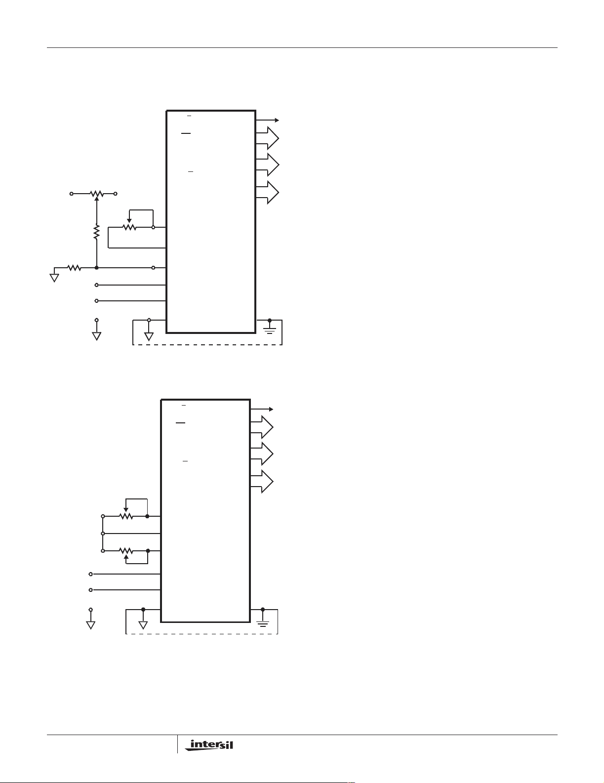
FIGURE 1. UNIPOLAR CONNECTIONS
HIGH BITS
MIDDLE BITS
LOW BITS
-15V 11
†
DIG COM 15
STS 28
24-27
20-23
16-19
+5V 1
+15V 7
ANALOG
INPUTS
±5V
±10V
R2
R1
GAIN
100Ω
100Ω
OFFSET
212/8
3CS
4A
O
5R/C
6CE
10 REF IN
8REFOUT
12 BIP OFF
13 10V
IN
14 20V
IN
9 ANA
COM
Range Connections and Calibration Procedures
The HI-X74A is a “complete” A/D converter, meaning it is fully
operational with addition of the power supply voltages, a Start
Convert signal, and a few external components as shown in
Figure 2 and Figure 3. Nothing more is required for most
applications.
Whether controlledby a processor or operating in the standalone mode, the HI-X74A offers four standard input ranges:
0V to +10V,0V to +20V,±5V and ±10V. The maximum errors
forgain and offset ar e listed under Specifications.If required,
however, these errors may be adjusted to zero as explained
below. Power supply and ground connections have been
discussed in an earlier section.
Unipolar Co nn ections an d Calibration
Refer to Figure 2. The resistor s shown (see Note below)
are for calibration of offset and gain. If this is not req ui red,
replaceR2witha50Ω, 1% m etal film resi stor and remove
the network on pin 12. C onnect pin 12 t o pin 9. Then,
connect the analog si gnal t o pin 13 for the 0V t o 10V range,
or to pin 14 for the 0V to 20V range. Inputs to +20V (5V
over the power supply) are no problem - the con v ert er
operates normally.
Calibration consists of adjusting the converter’s most
negative output to its ideal val ue (offset adjustment), then,
adjusting the mos t positive output to its ideal value (g ain
adjustment). To understand the procedure, note that in
principle, one is setting the out put with respect to the
midpoint of an increment of anal og input, as denoted by
two adjacent code changes. Nominal value of an in cre men t
is one LSB. How ever, this approach is impractical because
nothing “happens” at a midpoint to ind icate that an
adjustment is complete. Therefore , c ali br ation is performed
in terms of the observable code changes instead of the
midpoint bet ween code changes.
Forexample,midpointofthefirstLSBincrementshouldbe
positioned at the origin, wi th an output code of all 0’s. To do
this, apply an input of +
+2.44mV for the 20V range). Adjust the Offset potentiometer
R1 until the first code transition flickers between
0000 0000 0000 and 0000 0000 0001.
Next, perform a Gain Adjust at positive full scale. Again, the
ideal input corresponding to the last c ode change is applied.
This is 1
1
/2LSBs below the nominal full scale (+9.9963V for
10V range; +19.9927V for 20V range). Adjust the Gain
potentiometer R2 for flicker between codes 1111 1111 1110
and 1111 1111 1111.
1
/2LSB (+1.22mV for the 10V range;
†When driving the 20V (pin 14) input, minimize capacitance on pin 13.
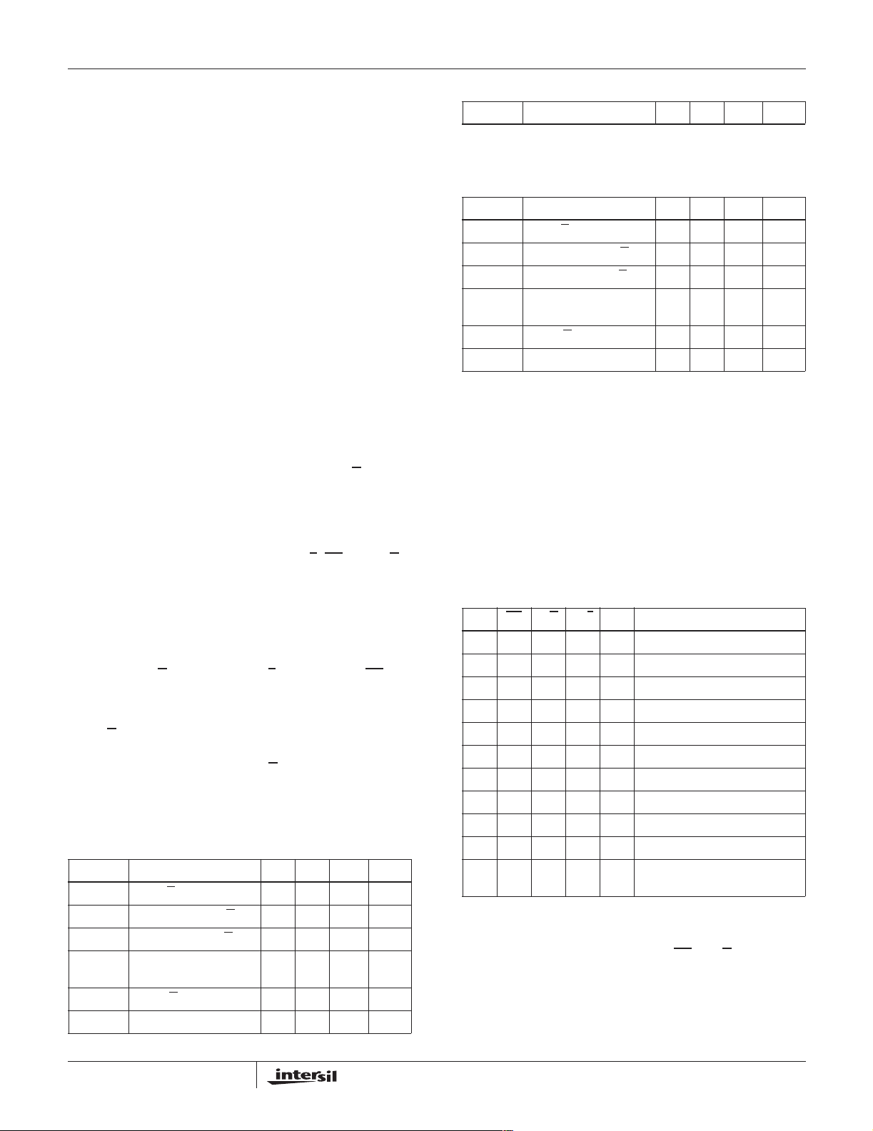
FIGURE 2. BIPOLAR CONNECTIONS
Bipolar Connections and Calibration
Refer to Figure 3. The ga in and offset er rors listed under
Specifications may be adjusted to zero using
potentiometers R1 and R 2 (see Note below). I f this isn’t
required, either or both pots m ay be replaced by a 50Ω,1%
metal film resistor.
10
Page 11
HI-574A, HI-674A
www.BDTIC.com/Intersil
Connect the Analog signal to pin 13 for a ±5V range, or to
pin14fora±10V range. Calibration of offset and gain is
similar to that for the unipolar ranges as discussed above.
First apply a DC input voltage
1
/2LSB above negative full
scale (i.e., -4.9988V for t he ±5V range, or -9.9976V for the
±10V range). Adjust the offset potentiometer R1 for flicker
between output codes 0000 0000 0000 and 0000 0000
0001. Next, apply a DC input voltage 1
1
/2LSBs below
positivefull scale (+4.9963V for ±5V range; +9.9927V for
±10V range). Adjust the Gain potentiometer R2 for flicker
between codes 1111 1111 1110 and 1111 1111 1111.
NOTE: The 100Ω potentiometer R2 provides Gain Adjust for the 10V
and 20V ranges. In some applications, a full scale of 10.24V (LSB
equals 2.5mV) or 20.48V (LSB equals 5.0mV) is more convenient.
For these, replace R2 by a 50Ω, 1% metal film resistor. Then, to provideGain Adjust for the 10.24V range, add a 200Ω potentiometer in
series with pin 13. For the 20.48V range, add a 500Ω potentiometer
in series with pin 14.
Controlling the HI-X74A
The HI-X 74A includes logic for direct interf ace to most
microprocessor systems. Th e processor may take full
control of eac h conversion, or the converter may operate in
the “stand-a lone” mode, controlled only by the R/C
Full cont rol consists of s elect ing an 8-bit or 12-bit
conversion cycle, initiating the conversi on, and reading the
output data when ready-choosi ng either 12 bits at once or 8
followed by 4, in a left-justified format. The five contro l
inputs are all TTL/CMOS-compatible: (12/ 8
,CS,AO,R/C
and CE). Table 1 illustrates the use of these inputs in
controlling the convert er’s o perat i ons. Also, a s impl ified
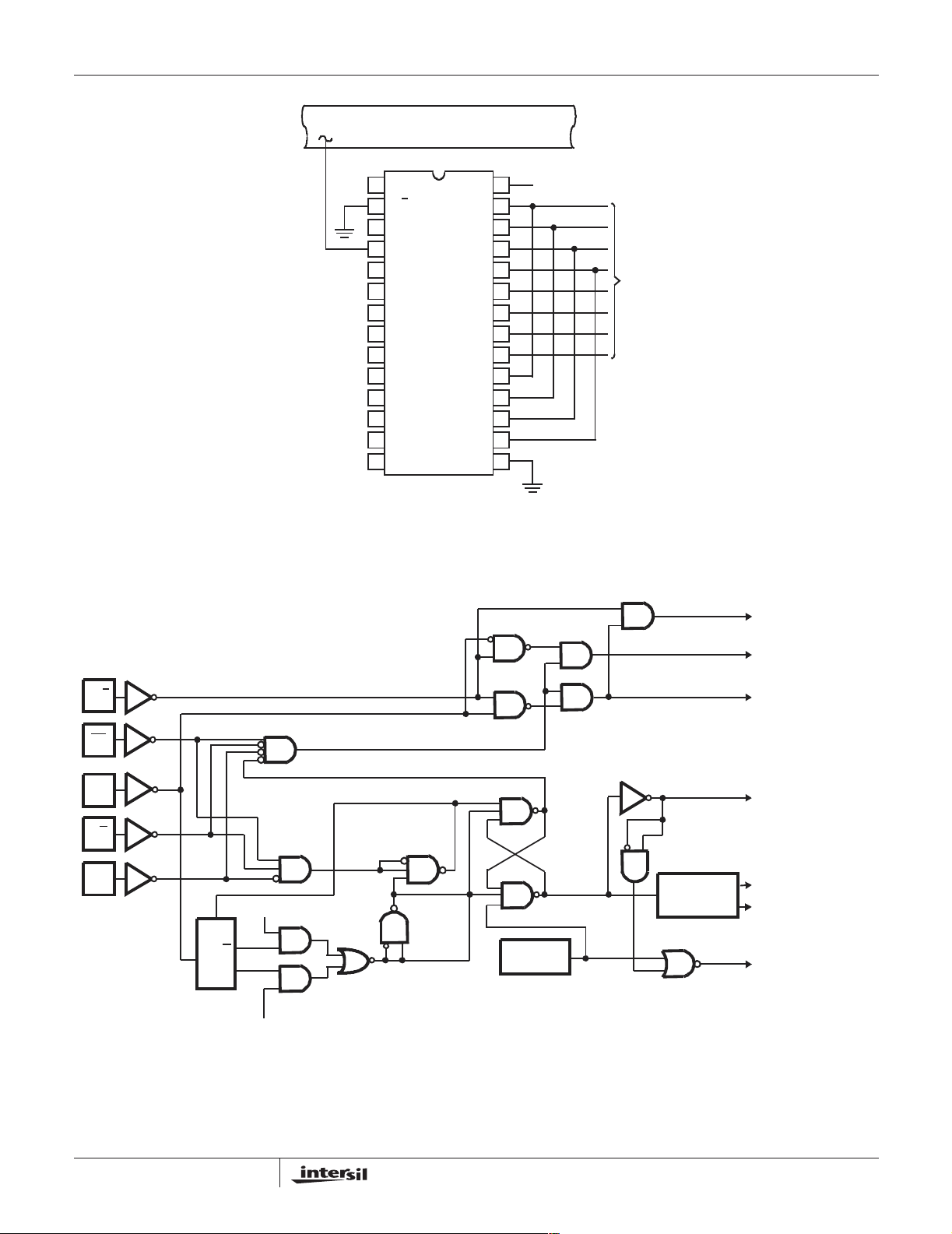
schematic of the internal control logic is shown in F ig ure 7.
“Stand-Alone Operation”
The simplest control interface calls for a single control line
connectedto R/C
A
are wired low, and the output data appears in words of
O
12 bits each.
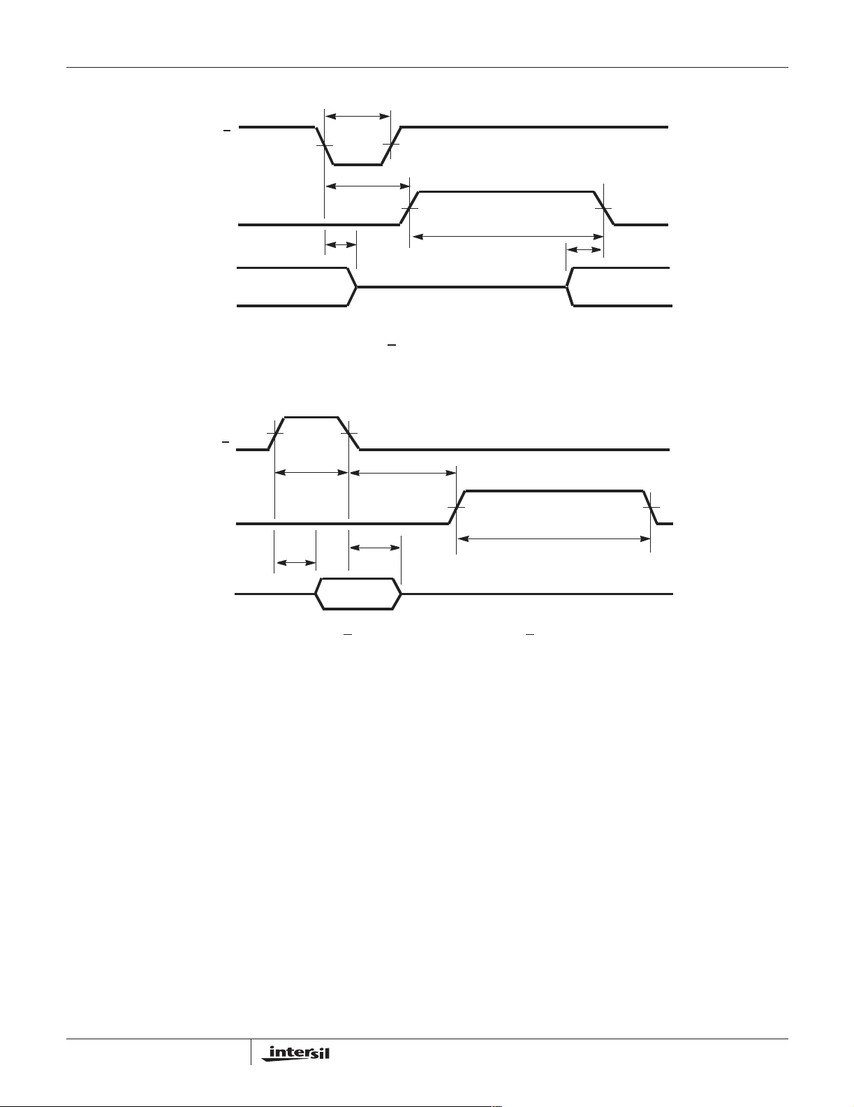
The R/C
signal may have any duty cycle within (and
including)the extremes shown in Figures 8 and 9. In
general, data may be read when R/C
also high, indicating a conversion is in progress. Timing
parametersparticular to this mode of operation are listed
below under “Stand-Alone Mode Timing”.
SYMBOL PARAM ETER MIN TYP MAX UNITS
t
HRL
t
DS
t
HDR
t
HS
t
HRH
t
DDR
. Als o, CE and 12/8 are wired high, CS and
is high unless STS is
HI-574A STAND-ALONE MODE TIMING
Low R/C Pulse Width 50 - - ns
STS Delay fromR/C --200ns
Data Valid after R/C Low 25 - - ns
STS Delay afterData
Valid
High R/C PulseWidth 150 - - ns
Data Access Time - - 150 ns
300 - 1200 ns
input.
HI-574A STAND-ALONE MODE TIMING
SYMBOL PARAM ETER MIN TYP MAX UNITS
Time is measured from 50% level of digital transitions. Tested with
a 50pF and 3kΩ load.
HI-674A STAND-ALONE MODE TIMING
SYMBOL PARAM ETER MIN TYP MAX UNITS
t
t
t
t
Time is measured from 50% level of digital transitions. Tested with
a 50pF and 3kΩ load.
Low R/C Pulse Width 50 - - ns
HRL
t
STS Delay from R/C --200ns
DS
Data Valid after R/C Low 25 - - ns
HDR
t
STS Delay afterData
HS
Valid
High R/C Pulse Width 150 - - ns
HRH
Data Access Time - - 150 ns
DDR
25 - 850 ns
Conversion Length
A Convert Starttransition (see Table1) latches the state of
A
, which determines whether the conversion continues for
O
12 bits (A
low)or stopswith 8 bits (AOhigh).If all 12 bitsare
O
read following an 8-bit conversion, the last three LSBs will
read ZERO and DB3 will read ONE. A
is latched because it
O
is also involved in enabling the output buffers (see “Reading
the Output Data”). No other control inputs are latched.
TABLE 1. TRUTH TABLE FOR HI-X74A CONTROL INPUTS
CE CS
0XXXXNone
X1XXXNone
↑ 0 0 X 0 Initiate 12-bit conversion
↑ 0 0 X 1 Initiate 8-bit conversion
1 ↓ 0 X 0 Initiate 12-bit conversion
1 ↓ 0 X 1 Initiate 8-bit conversion
10↓ X 0 Initiate 12-bit conversion
10↓ X 1 Initiate 8-bit conversion
1011XEnable12-bitOutput
10100Enable8MSBsOnly
10101Enable4LSBsPlus4Trailing
R/C 12/8 A
O
Zeroes
OPERATION
Conversion Start
A conversion may be initiatedas shown in Table 1 by a logic
transitionon any of three inputs: CE, CS
the three to reach the correct state starts the conversion,so
one, two or all three may be dynamically controlled. The
nominal delay f rom each is the same, and i f necessary, all
three may change state simultaneously. However, to ensure
or R/C. The last of
11
Page 12
HI-574A, HI-674A
www.BDTIC.com/Intersil
that a particular input controls the start of conversion, the
other two should be set up at least 50ns earlier. See the
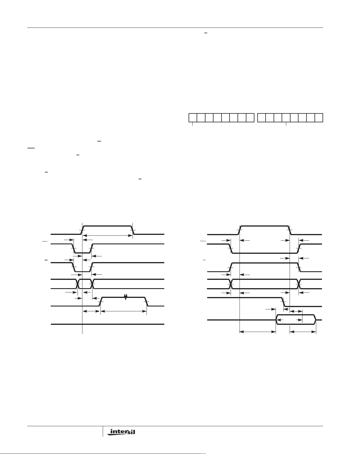
HI-X74A TimingSpecifications, Convert Mode.
This variety of HI-X74A control modes allows a simple
interface in m ost system applications.The Convert Start
timing relationships are illustrated i n Figure 4.
The output signal STS indicates status of the converter by
going high only while a conversion is in progress. While STS
is high, the output buffers remain in a high impedance state
and data cannot be read. Also, an additionalStart Convert
will not reset the converter or reinitiate a conversion while
STS is high.
Reading the Output Data
The output data buffers remain in a high impedance state
untilfour conditions ar e met: R/ C
CS
low. At that time, data lines become active according to
the state of inputs 12/8
and AO. Timing constraints are
illustrated in Figure 5.
The 12/8
input will be tied high or low in most applications,
though it is fully TTL/CMOS-compatible.With 12/8
12 output lines becomeactivesimultaneously, for interfaceto
a 12-bit or 16-bit data bus. The A
high,STS low,CE high and
high, all
input is ignored.
O
With 12/8
selected one at a time by A
to be connected as shown in Figure 6. A
low,the output is organized in two 8-bit bytes,
. This allows an 8-bit data bus
O
is usually tied to
O
the least significant bit of the address bus, for storing the
HI-X74A output in two consecutive memory locations. (With
A
low,the 8 M SBs only are enabled.With AOhigh,4 MSBs
O
are disabled, bits 4 through7 are forced low,and the 4 LSBs
areenabled). This two byteformat is considered“left justified
data,”f or which a decimal (orbinary!)point isassumed tothe
left of byte 1:
BYTE 1 BYTE 2
XXXXXXXX XXXX0000
•
MSB LSB
Further, A
may be toggled at any time without damage to
O
the converter. Break-before-makeaction is guaranteed
between the two data bytes, which assures that the outputs
strapped together in Figure 6 will never be enabled at the
same time.
A read operation usually begins after the conversion is
complete and STS is low. For earliest access to the data,
however, the read should begin no later than (t
DD+tHS
)
before STS goes low. See Figure 5.
t
CE
t
SSC
CS
t
SRC
R/C
t
A
STS
DB11-DB0
See HI-X74A Timing Specifications for more information.
HRC
O
t
SAC
t
HAC
t
DSC
HIGH IMPEDANCE
FIGURE 3. CONVERT START TIMING
HEC
t
HSC
t
C
CE
t
CS
R/C
A
O
STS
DB11-DB0
See HI-X74A Timing Specifications for more information.
FIGURE 4. READ CYCLE TIMING
SSR
t
SRR
t
SAR
HIGH IMPEDANCE
t
HSR
t
HRR
t
HAR
t
HS
DATA
VALID
t
DD
t
HD
t
HL
12
Page 13
HI-574A, HI-674A
www.BDTIC.com/Intersil
A
O
ADDRESS BUS
1
2
12/8
3
4
A
O
5
6
7
8
9
10
11
12
13
14
DB11 (MSB)
HI-X74A
DB0 (LSB)
STS
DIG.
COM.
28
27
26
25
24
23
22
21
20
19
18
17
16
15
FIGURE 5. INTERFACE TO AN 8-BIT DATA BUS
DATA
BUS
INPUT BUFFERS
12/8
CS
A
O
R/C
CE
A
CK
D
LATCH
O
NIBBLE B ZERO
OVERRIDE
NIBBLE A, B
NIBBLE C
READ CONTROL
STA TUS
CONVERT
EOC9
Q
Q
EOC13
CONTROL
POWER UP
RESET
CURRENT
CONTROLLED
OSCILLATOR
STROBE
CLOCK
RESET
FIGURE 6. HI-X74A CONTROL LOGIC
13
Page 14
R/C
www.BDTIC.com/Intersil
STS
HI-574A, HI-674A
t
HRL
t
DS
t
HDR
t
C
t
HS
DB11-DB0
DATA
VALID
FIGURE 7. LOW PULSE FOR R/C - OUTPUTS ENABLED AFTER CONVERSION
R/C
t
HRH
STS
t
DDR
DB11-DB0
FIGURE 8. HIGH PULSE FOR R/C
DATA
VALID
t
DS
t
C
HIGH-ZHIGH-Z
DATA
VALID
t
HDR
- OUTPUTS ENABLED WHILE R/C HIGH, OTHERWISE HIGH-Z
14
Page 15
Die Characteristics
www.BDTIC.com/Intersil
HI-574A, HI-674A
DIE DIMENSIONS:
Analog: 3070mm x 4610mm
Digital:1900mm x 4510mm
METALLIZATION:
Digital Type: Nitrox
Thickness: 10k
Å ±2kÅ
Metal 1: AlSiCu
Thickness: 8k
Å ±1kÅ
Metal 2: AlSiCu
Thickness: 16k
Å ±2kÅ
Analog Type:Al
Thickness: 16k
Å ±2kÅ
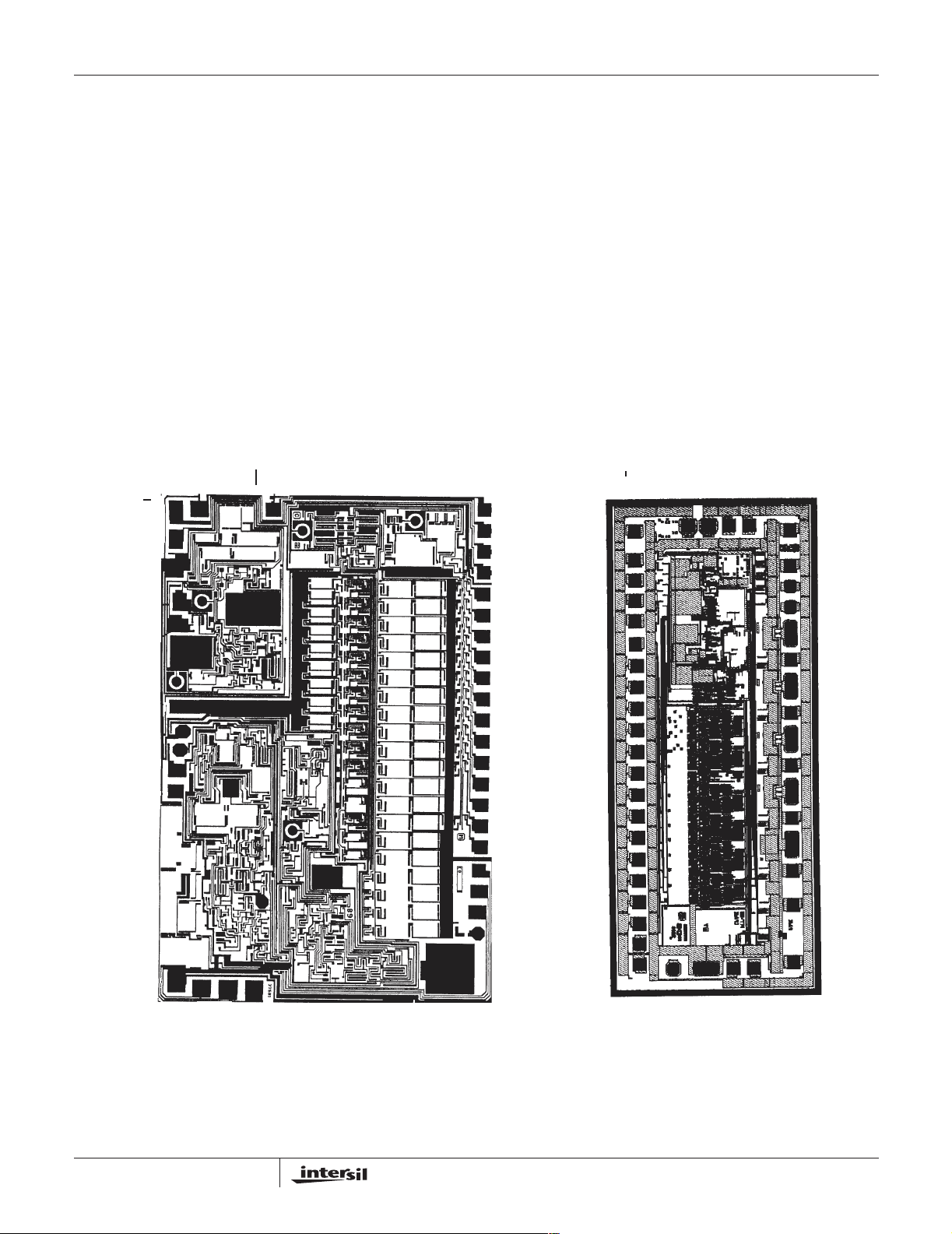
Metallization Mask Layout
O
V
A
R/C
CE
CC
CS
PASSIVATION:
WORST CASE CURRENT DENSITY:
HI-574A, HI-674A
Type: Nitride Over Silox
Nitride Thickness: 3.5k
Å ±0.5kÅ
Silox Thickness: 12kÅ ±1.5kÅ
5
2
1.3 x 10
A/cm
LOGIC
12/8
V
LOGIC
V
STS
DB11
DB10
DB9
V
REFOUT
ANALOG
COMMON
ANALOG
COMMON
ANALOG
COMMON
V
REFIN
V
EE
DB8
DB7
DB6
DB5
DB4
DB3
DB2
IN
10VIN20V
OFFSET
BIPOLAR
DB0
DB1
DIGITAL
COMMON
15
Page 16
HI-574A, HI-674A
www.BDTIC.com/Intersil
Ceramic Dual-In-Line Metal Seal Packages (SBDIP)
c1
LEAD FINISH
-A-
-B-
S
bbb C A - B
BASE
PLANE
SEATING
PLANE
S1
b2
ccc
CA-BM
NOTES:
1. Index area: A notch or a pin one identification mark shall be located adjacent to pin one and shall be located within the shaded
area shown. The manufacturer’s identification shall not be used
as a pin one identification mark.
2. The maximum limits of lead dimensions b and c or M shall be
measured at the centroid of the finished lead surfaces, when
solder dip or tin plate lead finish is applied.
3. Dimensions b1 and c1 apply to lead base metal only. Dimension
M applies to lead plating and finish thickness.
4. Cornerleads (1, N, N/2 , and N /2+1)may be configuredwith a
partial lead paddle.Forthis configurationdimension b3 replaces
dimension b2.
5. DimensionQshallbemeasuredfromtheseatingplanetothe
baseplane.
6. Measuredimension S1 at all fourcorners.
7. Measure dimension S2 from the top of the ceramic body to the
nearest metallization or lead.
8. N is the maximum number of terminal positions.
9. Braze fillets shall be concave.
10. Dimensioningand tolerancingper ANSI Y14.5M - 1982.
11. Controlling dimension: INCH.
D
A
A
b
e
DS S
-DBASE
E
S
S
D
Q
S2
-C-
aaa CA-BM DS S
METAL
b1
M
(b)
SECTION A-A
A
L
eA/2
(c)
M
eA
c
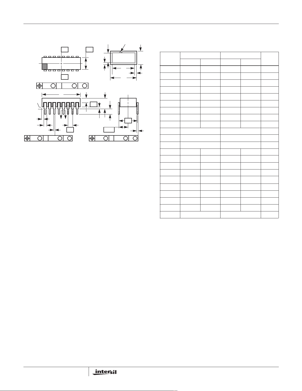
D28.6 MIL-STD-1835 CDIP2-T28 (D-10, CONFIGURATION C)
28 LEAD CERAMIC DUAL-IN-LINE METAL SEAL PACKAGE
INCHES MILLIMETERS
SYMBOL
A - 0.232 - 5.92 -
b 0.014 0.026 0.36 0.66 2
b1 0.014 0.023 0.36 0.58 3
b2 0.045 0.065 1.14 1.65 b3 0.023 0.045 0.58 1.14 4
c 0.008 0.018 0.20 0.46 2
c1 0.008 0.015 0.20 0.38 3
D - 1.490 - 37.85 -
E 0.500 0.610 12.70 15.49 -
e 0.100 BSC 2.54 BSC -
eA 0.600 BSC 15.24 BSC -
eA/2 0.300 BSC 7.62 BSC -
L 0.125 0.200 3.18 5.08 -
Q 0.015 0.060 0.38 1.52 5
S1 0.005 - 0.13 - 6
S2 0.005 - 0.13 - 7
o
α
aaa - 0.015 - 0.38 bbb - 0.030 - 0.76 -
ccc - 0.010 - 0.25 -
M - 0.0015 - 0.038 2
N28 288
90
105
o
90
o
105
NOTESMIN MAX MIN MAX
o
Rev. 0 5/18/94
-
16
Page 17
Dual-In-Line Plastic Packages (PDIP)
www.BDTIC.com/Intersil
HI-574A, HI-674A
N
D1
-C-
E1
-B-
A1
A2
E
A
L
e
C
C
L
e
A
C
e
B
INDEX
AREA
BASE
PLANE
SEATING
PLANE
NOTES:
1. Controlling Dimensions: INCH. In case ofconflictbetweenEnglishand
Metricdimensions, the inch dimensionscontrol.
2. Dimensioningand tolerancingper ANSI Y14.5M-1982.
3. Symbolsaredefinedin the “MO Series Symbol List” in Section2.2 of
Publication No. 95.
4. Dimensions A, A1 and L are measured with the packageseated in
JEDECseating plane gauge GS-3.
5. D, D1, and E1 dimensionsdo not include mold flashor protrusions.
Mold flash or protrusions shallnot exceed 0.010 inch (0.25mm).
6. E and aremeasuredwiththe leadsconstrainedtobe perpendicular to datum .
7. e
e
8. B1 maximumdimensionsdonot includedambar protrusions.Dambar
protrusions shall not exceed 0.010 inch (0.25mm).
9. N is the maximum number of terminal positions.
10. Cornerleads(1,N, N/2 and N/2 + 1) for E8.3, E16.3,E18.3,E28.3,
E42.6 will have a B1 dimension of 0.030 - 0.045 inch (0.76 - 1.14mm).
12 3 N/2
-A-
D1
B1
B
e
A
and eCare measured at the lead tips with the leads unconstrained.
B
must be zero or greater.
C
D
e
0.010 (0.25) C AM BS
-C-
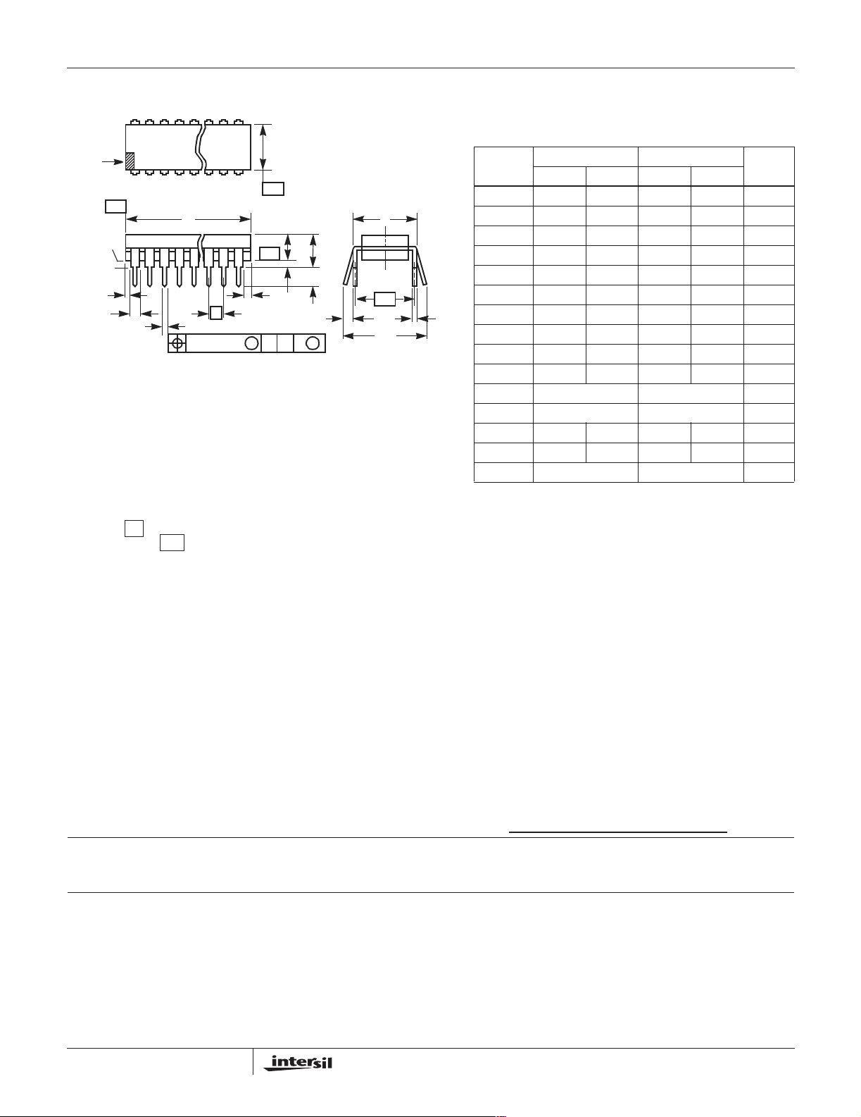
E28.6 (JEDEC MS-011-AB ISSUE B)
28 LEAD DUAL-IN-LINE PLASTIC PACKAGE
INCHES MILLIMETERS
SYMBOL
A - 0.250 - 6.35 4
A1 0.015 - 0.39 - 4
A2 0.125 0.195 3.18 4.95 -
B 0.014 0.022 0.356 0.558 B1 0.030 0.070 0.77 1.77 8
C 0.008 0.015 0.204 0.381 D 1.380 1.565 35.1 39.7 5
D1 0.005 - 0.13 - 5
E 0.600 0.625 15.24 15.87 6
E1 0.485 0.580 12.32 14.73 5
e 0.100 BSC 2.54 BSC e
A
e
B
L 0.115 0.200 2.93 5.08 4
N28 289
0.600 BSC 15.24 BSC 6
- 0.700 - 17.78 7
NOTESMIN MAX MIN MAX
Rev. 1 12/00
All Intersil productsare manufactured, assembled and tested utilizing ISO9000 quality systems.
Intersil Corporation’s quality certificationscan be viewed at website www.intersil.com/design/quality/iso.asp
Intersil products are sold by description only. Intersil Corporation reserves the right to make changes in circuit design and/or specifications at any time without notice.
Accordingly, the reader is cautionedto verify that data sheets are current before placing orders. Information furnished by Intersil is believed to be accurate and reliable.However, no responsibility is assumed by Intersil or its subsidiaries for its use; nor for any infringements of patents or other rights of third parties which may result from its use.
No license is granted by implication or otherwise under any patent or patent rights of Intersil or its subsidiaries.
For information regarding Intersil Corporation and its products, see web site www.intersil.com
Sales Office Headquarters
NORTH AMERICA
Intersil Corporation
2401 Palm Bay Rd.
Palm Bay, FL 32905
TEL: (321) 724-7000
FAX: (321) 724-7240
EUROPE
Intersil SA
MercureCenter
100,RuedelaFusee
1130 Brussels, Belgium
TEL: (32) 2.724.2111
FAX: (32) 2.724.22.05
17
ASIA
Intersil Ltd.
8F-2,96, Sec. 1, Chien-kuo North,
Taipei, Taiwan 104
Republic of China
TEL: 886-2-2515-8508
FAX: 886-2-2515-8369
.
 Loading...