

Page 1
HI-6010
GENERALDESCRIPTION
TheHI-6010isaCMOSintegratedcircuitdesignedto
interfacetheavionicsdatabusstandardARINC429toan
8bitport.Itcontainsonereceiverandonetransmitter.
Theyoperateindependentlyexceptfortheselftestoption
andtheparityoption.Thereceiverdemandsthatthe
incomingdatameetthestandardprotocolandthe
transmitteroutputsastandardprotocolstream.
TheHI-6010providesflexibleoptionsforinterfacingtothe
usersystem.Thecontrollingprocessorcanoperateboth
thereceiverandtransmittereitherbyusinghardwired
flagsandgatesatthepinsorbyusingsoftwa rereadsand
writesoftheStatusRegisterandControlRegisterora
combinationthereof.
Thechipisprogrammabletooperatewithsingle8bit
bytesrequiring"ontheflytransmitterloadingandreceiver
downloading"ortooperatein32bit"extendedbuffer"
mode.Inadditionthereisanoptiontouseautomaticlabel
recognitionafterloading8possiblelabelsforcomparison.
Parityandselftestarealsosoftwareprogrammable.
MasterResetisactivatedonlybytakingtheMRpinhigh.
Twoclockinputsallowindependentselectionofthedata
ratesofthetransmitterandreceiver.Eachmustb e4Xthe
desiredARINC429frequency.
Errorflagsaregeneratedfortransmitterunderwritesand
forreceiverdataframingmiscues,parityerrors,andbuffer
overwrites.
TheHI-6010isa5voltchipthatwillrequiredatatranslationfromandtotheARINCbus.TheHI-8482andHI-8588
linereceiversareavailableforthereceiversideandthe
HI-318X,HI-838XandHI-858Xlinedriversareavailable
forthetransmitterside.TheHI-8590isalsoavailablewith
alinedriverandalinereceiverinasingle16-pinthermally
enhancedESOICpackage.
FEATURES
!
ARINC429protocolcontrollerwithinterfaceto
an8bitbus
!
Automaticlabelrecognitionoption
!
8bitor32bitbufferingoption
!
Selftestandparityoptions
!
CMOS/TTLlogicpins
!
Plasticandceramicpackageoptions-surface
mountorDIP
!
Militaryprocessingavailable
PINCONFIGURATION (TopView)
28
V1
SS
WEF2
3
CTS
TXC4
HFS5
MR6
TXE7
RXRDY8
TXRDY9
TXD010
TXD111
RXC12
FCR13
RXD014
PinnumbersapplyforplasticandceramicDIPand
forplasticPLCC.Consultfactoryforpinoutof48
leadceramicleadlesschipcarrier.
RE
27C/
D
26
CS
25
WE
24D7
23D6
22D5
21D4
20D3
19D2
18D1
17D0
16RXD1
15V
DD
!
AvionicsDataCommunication
!
SerialtoParallelConversion
!
ParalleltoSerialConversion
HOLTINTEGRATEDCIRCUITS
(DS6010Rev.A)01/014-3
!
VDD=5.0VOLTS±5%
!
VSS=0.0VOLTS
Page 2
HI-6010
PINSYMBOLFUNCTIONDESCRIPTION
1VPOWER0.0Volts
2WEFOUTPUTErrorindicationifhigh.Statusregistermustbereadtodeterminespecificerror.
3INPUTEnablesdatatransmissionwhenlow.
4TXCINPUTSourceclockfordatatransmission.4timesbitrate.
5HFSINPUTHardwarefeatureselect.
6MRINPUTMasterreset,activehigh.
7TXEOUTPUTLowwhentransmissioninprogress.
8RXRDYOUTPUTHighwhendataofreceivedwordisavailable.
9TXRDYOUTPUTHighwhendataofatransmittedwordmaybeinput.
10TXD0OUTPUT"Zeroes"dataoutputoftransmitter.
11TXD1OUTPUT"Ones"dataoutputoftransmitter.
12RXCINPUTSourceclockf ordatareception.4timesbitrate.
13FCROUTPUTFirstcharacterreceivedflag.
14RXD0INPUT"Zeroes"datainputtoreceiver.
15VPOWER5Volts±5%
16RXD1INPUT"Ones"datainputtoreceiver.
17D0I/ODatabus
18D1I/ODatabus
19D2I/ODatabus
20D3I/ODatabus
21D4I/ODatabus
22D5I/ODatabus
23D6I/ODatabus
24D7I/ODatabus
25INPUT8bitdatabusinputcontrolactivelow.
26INPUTChipselect,activelow.
27C/INPUTHighforcontrolorstatusregisteroperations,lowfordata
28INPUT8bitdatabusoutputcontrol,activelow.
SS
CTS
DD
WE
CS
D
RE
Thereceiverlogicisindependentofthetransmitterexceptin
thefollowingways:
1.SelfTest
2.ParityOption
Inselftest,thetransmitteroutputsroutetothereceiverinputs
internallyignoringtheexternalinputs.Alsoinselftest,the
externalreceiverclockisreplacedwiththetransmitterclock.
Theparityoptionaffectsboththereceiverandtransmitter.
Eitherbothareoperationalorneither.
HARDWARECONTROLOFTHERECEIVER
PIN2-WEF
WEFisanerrorindicator.Itgoeshighforatransmitter
"underwrite"(failuretokeepupwithbyteloading)andpin2
HOLTINTEGRATEDCIRCUITS
goeshighforanyoneofthreereceivererrors.Thestatus
registerwillshowwhichofthethreeerrorsoccurred:
StatusRegisterBitError
SR3Receivedaparityerror
SR4DataOverwritten
SR5Receivingsequenceerror
ThepossibleReceiversequenceerrorsare:
1.RXD0andRXD1simultaneouslyaone.
2.Lessthan32bitsbefore3nulls.
3.Morethan32bits.
Therearenoerrorsflaggedforlabelsreceivedthatdon't
matchstoredlabelswheninthelabelrecognitionmode.
ErrorsareclearedbyMRorbyreadingtheStatusRegister.
PIN5-HFSandtheCONTROLREGISTER
Thispin,alongwiththecontrolregister,setsupthe
functioning(e.g.modes)ofthechip.IfH FSislow,the
4-4
Page 3
HI-6010
PIN14-RXD0andPIN16-RXD1
receiverisnotprogrammabletothe32bit"extendedbuffer"
modenortothelabelrecognitionmode.Affectingthe
receiver:
CONTROLPROGRAMPIN5
BITNAMEVALUEVALUE OPERATION
CR1X0Noaction
01Noaction
11Next8datareadcycleswillread
storedlabels.Onetimeonlysequence
oneachtransitonofCR1toa1.
CR20XReceiverisdisabled
1XReceiverisenabled
CR3*0XRXRDYgoeshighnormally
1XBlocksRXRDYforoneARINCword
CR40XSelftestdisabled
1XSelftestenabled
CR500Noparityerrorsenabledand32nd
bitisdata
10Parityerrorflagenabled
0132bit"extendedmode"enabledand
parityenabled.
118bit"onebyteatatime"modeand
parityenabled.
CR7X0Labelrecognitionnotprogrammable
01Labelrecognitiondisabled
11Labelrecognitionenabled
*CR3willbeautomaticallyresetto0afterbeingprogrammed
toa1atthecompletionofanARINCwordreception.This
allowsasoftwarelabelrecognitiondifferentfromtheautomatic
optionavailable.
Thesepinsmustbe5voltlogiclevels.Theremustbea
translatorbetweentheARINCbusandtheseinputs.
Typicallyareceiverchip,suchastheHI-8482orHI-8588
isinsertedbetweentheARINCbusandthelogicchips.
RXD0islookingforahighlevelforzeroinputsandRXD1is
lookingforahighlevelforoneinputs.Whenbothinputsare
lowthisisreferredtoastheNullstate.
SOFTWARECONTROLOFTHERECEIVER
BywritingtotheControlRegisterandreadingtheStatus
Registerthecontrollingprocessorcanoperatethereceiver
withouthardwareinterrupts.TheControlRegisterin
combinationwiththewiringofpin5wasexplained above.
TheStatusRegisterbitspertainingtothereceiverare
explainedbelow:
STATUSBITVALUEMEANING
SR10Noreceiverdata
1Receiverdataready
SR30Noparityerror
1Parityerror-Paritywaseven
SR40Receiverdatanotoverwritten
1Receiverdatawasoverwritten
SR50Receiverdatareceivedwithoutframingerror
1Framingerror-Didnotreceiveexactly32
goodbits
SR60Didnotreceivefirstbyte
1Receivedfirstbyte-Sameflagaspin13
COMMUNICATINGWITHTHECONTROLAND
STATUSREGISTERS
PIN6-MR
WhenMRisa1,thecontrolwordissetto0X100101(CR7CR0).Forthereceiverthissetsup8bitmodewiththe
receiverandparityenabled.MRalsoinitializestheregisters
andlogic.ThefirstARINCreceptionwillonlyoccura
after
wordgap.
PIN8-RXRDY
In8bitmode,thispingoeshighwhenever8bitsarereceived
withouterror.In32bitmodethispingoeshighafterall32bits
arereceivedwithnoerror.Thisflagmaybeinhibitedforone
ARINCwordifCR3isprogrammedto1.Thisflagisalso
inhibitedinlabelrecognitioniftheincomingARINClabeldoes
notmatchoneofthestored8labels.
PIN12-RXC
Thispinmusthaveaclocka ppliedthatis4Xthedesired
receivefrequency.
PIN13-FCR
In8bitmode,thispinflagsthefirstcharacter(byte)received.
In32bitmode,thispingoeshighforavalid32bitword.The
pinisnotaffectedbyCR3programming.
Pin27,C/,mustbehightoreadthestatusregisterorwrite
D
thecontrolregister.Readingthestatusregisterresets
errors.Thereisnoprovisiontoreadthecontrolregister.
LABELRECOGNITIONOPTION
Pin5mustbehighiflabelrecognitionisselectedineitherthe
8or32bitmodesandalleightlabelbuffersmustbewritten
usingredundantlabels,ifnecessary.
Thechipcomparestheincominglabeltothestoredlabels.If
amatchisfound,thedataisprocessed.Ifamatchisnot
found,noindicatorsofreceivingARINCdataarepresented.
LOADINGLABELS
AfterthewritethatchangesCR7from0to1,thenext8writes
ofdata(C/isazerofor data)willloadthelabelregisters.
D
Labelsmustbeloadedwheneverpin5goesfromlowto
high.
READINGLABELS
AfterthewritethatchangesCR1from0to1,thenext8data
readsarelabels.
HOLTINTEGRATEDCIRCUITS
4-5
Page 4
HI-6010
PIN6-MR
Thetransmitterlogicisindependentofthereceiverexceptin
thefollowingways:
1.SelfTest
2.ParityOption
Inselftestthetransmitteroutputsroutetothereceiverinputs
internallyandtheTXD0andTXD1outputsareinhibited.
Whenparityisenabled,boththereceiverandtransmitterare
affected.Oddparityisautomaticallygeneratedinthe32nd
bitifthisoptionisselected.
HARDWARECONTROLOFTHETRANSMITTER
PIN2-WEF
Thisoutputgoeshighfor1transmittererrorand3receiver
errors.Todeterminewhicherrorisbeingflagged,readthe
StatusRegister.ReadingtheStatusRegisteralsoclearsthe
errorflag.Thetransmitte rwillnotfunctionuntiltheerroris
cleared.ItcanalsobeclearedbyMRgoinghigh.
Theonlypossibletransmittererrorisgeneratedwhenrunning
in8bitmode.Forthetransmitterthismeansloadingthelast3
byteswhilethetransmissionisinprogress.Failuretoloada
bytebeforethepreviousbyte's8thbitistransmittedwill
generatetheerror,indicatedbystatusbitSR7settoa1.
PIN3-
Thispinisahardwaregatefortransmissions.Ifthe
transmitterbufferisloadedandControlRegisterbitCR0isa
one,theonlyinhibitofthetransmitterwouldbefortobea
one.Whentakenlow,transmission ofanARINCwordis
enabled.Itmaybepulsedtoreleaseeachtransmittedword.
PIN4-TXC
Thedatarateoftransmissioniscontrolledbythispin.This
clockmustbe4Xthedesireddaterate.
PIN5-HFSandtheCONTROLREGISTER
CTS
CTS
Thechipisinitializedwheneverthispingoeshigh.The
ControlRegisterissetto0X100101(CR7-CR0).Forthe
transmitterthissetsup8bitmodewiththetransmitter
enabled.
PIN7-TXE
Wheneveratransmissionbegins,thispingoeslowand
returnshighafterthetransmissioniscomplete.
PIN9-TXRDY
WheneverTXRDYisaone,datamaybewrittenintothe
transmitterbuffer.In8bit"onebyteatatime"mode,thispin
maybemonitoredtoindicatewhentowritethenext8bits.
PIN10-TXD0andPIN11-TXD1
TXD0willgohighduringatransmissionifthedataiszero.
TXD1goeshighifdataisaone.Whenbothpinsarelowthis
isreferredtoastheNullstate .TypicallyanARINC
transmitterchip,suchastheHI-8382,HI-8383,HI-8585or
HI-8586isconnectedtothesepinstotranslatethe5volt
levelstotheproperARINCbuslevels.
SOFTWARECONTROLOFTHETRANSMITTER
BywritingintotheControlRegisterandreadingtheStatus
Register,thecontrollingprocessorcanoperatethe
transmitterindependentoftheflagsatthepins.
TransmissioncanbeinitiatedbychangingCR0froma0toa1
afterthetransmitterbufferhasbeenloaded.ThentheStatus
Registermaybemonitoredasfollows:
STATUSBITVALUEMEANING
SR00Donotloadthetransmitterbuffer
1Readytoloadthetransmitterbuffer
SR20Transmissioninprogress
1Transmitterisidle
SR70Notransmissionerror
18bitmodeonlyerrorforunderwritingdata
ThispinalongwiththeControlRegistersetsthefunctioningof
thechip.Forthetransmitter:
CONTROLPROGRAMPIN5
BITNAMEVALUEVALUE OPERATION
CR00XTransmitterisdisabled
1XTransmitterisenabled
CR40XNotinselftest
1XSelftestenabled
CR5008bitmode+datain32ndbit
108bitmode+parityenabled
0132bitmodewithparityenabled
118bitmodewithparityenabled
HOLTINTEGRATEDCIRCUITS
CablingNoise
thereforetheyaresusceptibletonoisenearground.Ifthedata
busispassedbyribboncableortheequivalenttothedevice
undertest,itispossibletogetsignificantglitchesontheMaster
Resetline.Theproblemwillappeartobeapatternsensitive
failure.OnecureissimplytoadequatelybypassMasterReset.
AnotheristobuffertheHI-6010inputsnearthechip.
ReceiverSeemsDead
receivermustseeawordgapbeforethefirstARINCdatabit.
ErrorflagsmustbeclearedbyeitheraStatusRegisterReador
byaMasterReset.Theoperati onofeitherthetransmitterorthe
receiverisinhibiteduponerror.
-TheHI-6010hasTTLcompatibleinputsand
-AfterMasterResettheHI-6010
4-6
Page 5

HI-6010
8BIT"ONEBYTEATATIME"TRANSMITUSINGTXRDY,PIN9,TOTRIGGERNEXTBYTELOAD
RE C/ D CS WE D7 D6 D5 D4 D3 D2 D1 D0
28272625242322212019181765378913COMMENTS
110P000*0000100X1X1XLoadControlWord
100PT0000X0XTXRDY&TXEGoLowAfterLoadData
1001XXXXXXXX0000X1XMonitorPin9toGoHigh
100PT0000X0XAfterPin9HighThenLoadNextByte
1001XXXXXXXX0000X1XMonitorPin9toGoHigh
100PT0000X0XLoad
1001XXXXXXXX0000X1XMonitorPin9toGoHigh
100PT0000X0XLoad
1011XXXXXXXX0001X1XTransmissionComplete
D8TD7TD6TD5TD4TD3TD2TD1
D16TD15TD14TD13TD12TD11TD10TD9
D24TD23TD22TD21TD20TD19TD18TD17
D32TD31TD30TD29TD28TD27TD26TD25
8BIT"ONEBYTEATATIME"TRANSMITMONITORINGSTATUSREGISTERBIT0
RE C/ D CS WE D7 D6 D5 D4 D3 D2 D1 D0
28272625242322212019181765378913COMMENTS
110P000*000010001X1XLoadControlWordD0=1
100PT0000X0XLoadDatatoTransmit-Byte1
P001000000000000X0XStatusBits0,2&7(
P001000000010000X1XStatusBit0GoesHigh
100PT0000X0XLoadtheNextBytetoTransmit
P001000000000000X0XMonitorStatusBit0
P001000000010000X1XDetectaTransition
100PT0000X0XLoad3rdByte
P001000000000000X0XMonitorStatusBit0
P001000000010000X1XDetectaTransition
100PT0000X0XLoad4thByte
D8TD7TD6TD5TD4TD3TD2TD1
TXRDY,TXE&ERROR)
D16TD15TD14TD13TD12TD11TD10TD9
D24TD23TD22TD21TD20TD19TD18TD17
D32TD31TD30TD29TD28TD27TD26TD25
HOLTINTEGRATEDCIRCUITS
4-7
Page 6

HI-6010
RECEIVING32BITWORDSHARDWAREINTERRUPT
RE C/ D CS WE D7 D6 D5 D4 D3 D2 D1 D0
28272625242322212019181765378913COMMENTS
110P0000010001XX0X0WriteCR:
1101XXXXXXXX01XX1X1AwaitPin8orPin13toGoHigh
P00101XX1X1Read1stByte
P00101XX1X1Read2ndByte
P00101XX1X1Read3rdByte
P00101XX1X1Read4thByte
1001XXXXXXXX01XX0X0
RD8RD7RD6RD5RD4RD3RD2RD1
RD16RD15RD14RD13RD12RD11RD10RD9
RD24RD23RD22RD21RD20RD19RD18RD17
PARRD31RD30RD29RD28RD27RD26RD25
32BitRecieve&NoLabelRecogn.
RECEIVING8BITMODESOFTWAREINTERRUPT
RE C/ D CS WE D7 D6 D5 D4 D3 D2 D1 D0
28272625242322212019181765378913COMMENTS
110P0010010001XX0X0WriteCR:
8BitReceive&NotLabelRecong.
P10100000X0001XX0X0MonitortheStatusRegister
P10101000X1001XX1X1SR1&SR6GoHigh-FirstCharacter
P00101XX0X0Read1stByte
P10100000X0001XX0X0LookforSR1toGoHighAgain
P10100000X1001XX1X0
P00101XX0X0Read2ndByte
P10100000X0001XX0X0LookforSR1toGoHighAgain
P10100000X1001XX1X0
P00101XX0X0Read3rdByte
P10100000X0001XX0X0LookforSR1toGoHighAgain
P10100000X1001XX1X0
P00101XX0X0Read4thByte
RD8RD7RD6RD5RD4RD3RD2RD1
RD16RD15RD14RD13RD12RD11RD10RD9
RD24RD23RD22RD21RD20RD19RD18RD17
PARRD31RD30RD29RD28RD27RD26RD25
HOLTINTEGRATEDCIRCUITS
4-8
Page 7

HI-6010
TRANSMITIN32BITMODE(EXTENDEDBUFFER)USINGTOINITIATECTS
RE C/ D CS WE D7 D6 D5 D4 D3 D2 D1 D0
28272625242322212019181765378913COMMENTS
110P000000010111X1XLoadControlWordD5=0&D0=1
100P0111X0XLoadDatatoTransmit-Byte1
100P0111X0XLoadDatatoTransmit-Byte2
100P0111X0XLoadDatatoTransmit-Byte3
100PXT0111X1XLoadDatatoTransmit-Byte4
1111XXXXXXXX0101X1XTakeLowtoStartTransmitting
TD8TD7TD6TD5TD4TD3TD2TD1
TD16TD15TD14TD13TD12TD11TD10TD9
TD24TD23TD22TD21TD20TD19TD18TD17
D31TD30TD29TD28TD27TD26TD25
CTS
32ndBitWillBeParity
TRANSMITIN32BITMODE(EXTENDEDBUFFER)
USINGSOFTWAREWRITETOCONTROLREGISTER
RE C/ D CS WE D7 D6 D5 D4 D3 D2 D1 D0
28272625242322212019181765378913COMMENTS
110P000000000101X1XLoadControlWordD5=0&D0=0
100P0101X0XLoadDatatoTransmit-Byte1
TD8TD7TD6TD5TD4TD3TD2TD1
100P0101X0XLoadDatatoTransmit-Byte2
100P0101X0XLoadDatatoTransmit-Byte3
100PXT0101X1XLoadDatatoTransmit-Byte4
110P000000010100X1XWriteControlWordD0=1
TD16TD15TD14TD13TD12TD11TD10TD9
TD24TD23TD22TD21TD20TD19TD18TD17
D31TD30TD29TD28TD27TD26TD25
32ndBitWillBeParity
HOLTINTEGRATEDCIRCUITS
4-9
Page 8

HI-6010
LOADINGLABELS
RE C/ D CS WE D7 D6 D5 D4 D3 D2 D1 D0
28272625242322212019181765378913COMMENTS
110P0000010001XXXXXControlBit7MustBe0First
110P1000010001XXXXXWrite1intoControlBit7
100P1L71L61L51L41L31L21L11L001XXXXXLoadthe1stLabel
100P2L72L62L52L42L32L22L12L001XXXXXLoadthe2ndLabel
100P3L73L63L53L43L33L23L13L001XXXXXLoadthe3rdLabel
100P4L74L64L54L44L34L24L14L001XXXXXLoadthe4thLabel
100P5L75L65L55L45L35L25L15L001XXXXXLoadthe5thLabel
100P6L76L66L56L46L36L26L16L001XXXXXLoadthe6thLabel
100P7L77L67L57L47L37L27L17L001XXXXXLoadthe7thLabel
100P8L78L68L58L48L38L28L18L001XXXXXLoadthe8thLabel
READINGLABELS
RE C/ D CS WE D7 D6 D5 D4 D3 D2 D1 D0
28272625242322212019181765378913COMMENTS
110P1000010001XXXXXMakeSureBit1ofControlWordis0
110P1000011001XXXXXWrite1intoControlBit1
P0011L71L61L51L41L31L21L11L001XXXXXReadthe1stLabel
P0012L72L62L52L42L32L22L12L001XXXXXReadthe2ndLabel
P0013L73L63L53L43L33L23L13L001XXXXXReadthe3rdLabel
P0014L74L64L54L44L34L24L14L001XXXXXReadthe4thLabel
P0015L75L65L55L45L35L25L15L001XXXXXReadthe5thLabel
P0016L76L66L56L46L36L26L16L001XXXXXReadthe6thLabel
P0017L77L67L57L47L37L27L17L001XXXXXReadthe7thLabel
P0018L78L68L58L48L38L28L18L001XXXXXReadthe8thLabel
HOLTINTEGRATEDCIRCUITS
4-10
Page 9
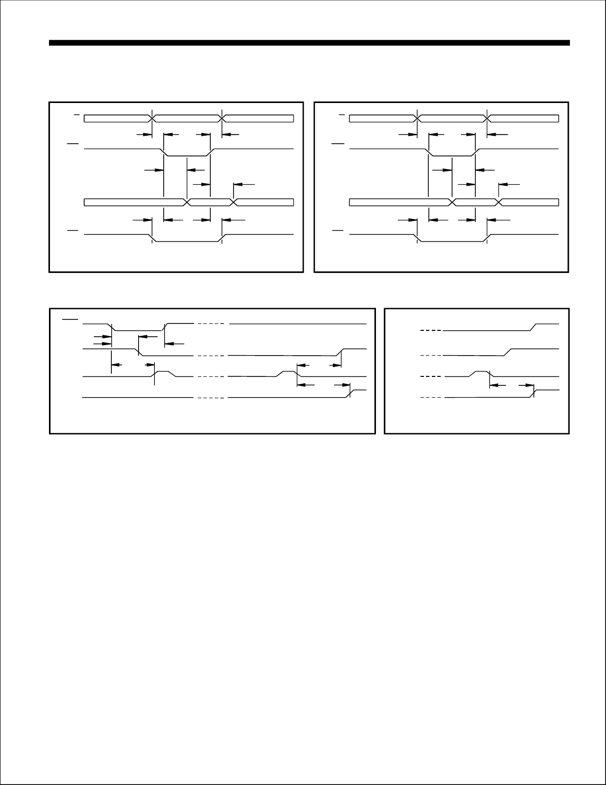
TIMINGDIAGRAMS
HI-6010
C/ D
RD
DATA
BUS
CS
CTS
TXE
TXD0/
TXD1
TXRDY
DATABUSTIMING-READ
VALID
t
CDH
t
DR
t
CSHR
t
CSSR
t
CDS
t
RD
VALID
Figure1. Figure2.
TRANSMTTEROPERATION RECEIVEROPERATION
t
CTL
t
CPW
t
ENDAT t
FIRST
BIT
LAST
BIT
DATABUSTIMING-WRITE
C/ D
t
CDS
WE
DATA
BUS
t
CSSW
CS
DTX
t
TXRY
RXD0/
RXD1
RXRDY/
FCR
VALID
t
t
DWH
CDH
t
CSHW
t
DR
WP
t
DWS
t
VALID
LAST
BIT
Figure3. Figure4.
HOLTINTEGRATEDCIRCUITS
4-11
Page 10

HI-6010
ABSOLUTEMAXIMUMRATINGS
(VoltagesreferencedtoV=0V)SS
SupplyVoltage:V-0.5Vto+7.0V
InputVoltageRangeV-0.5VtoV+0.5V
InputCurrentI+10mA
OutputCurrent+25mA
DD
INDD
IN
OUTI
PowerDissipationP500mW
OperatingTemperatureRange:T(Industrial)-40°Cto+85°C
StorageTemperatureRange:T-65°Cto+150°C
LeadTemperatureT300°Cfor60Seconds
D
A
T(Hitemp&Military)-55°Cto+125°C
A
STG
LEAD
NOTE:Stressesabovethoselistedunder"AbsoluteMaximumRatings"maycausepermanentdamagetothedevice.Thesea restressratings
only.Functionaloperationofthedeviceattheseoranyotherconditionsabovethoseindicatedintheoperationalse ctionsofthespecificationsis
notimplied.Exposuretoabsolutemaximumratingconditionsforextendedperiodsmayaffectdevicereliability.
DCELECTRICALCHARACTERISTICS
V=5.0V,V=0V,T=OperatingTemperatureRange(unlessotherwisespecified).DDSSA
PARAMETERSYMBOLCONDITIONMINTYPMAXUNITS
OperatingVoltageV4.555.5V
Min.InputVoltage(HI)V2.11.4V
Max.InputVoltage(LO)V1.40.7V
Min.InputCurrent(HI)IV=4.9V-1.5µA
Max.InputCurrent(LO)IV=0.1V1.5µA
Min.OutputVoltage(HI)VI=-1.5mA2.7V
Max.OutputVoltage(LO)VI=1.8mA0.7V
OperatingCurrentDrainIf=400KHz0.82.8mA
InputCapacitanceCNottested20pF
DD
IH
IL
IHIH
ILIL
OHOUT
IHOUT
DD
IN
ACELECTRICALCHARACTERISTICS
V=5.0V,V=0V,T=OperatingTemperatureRange(unlessotherwisespecified).DDSSA
PARAMETERSYMBOLMINTYPMAXUNITS
DATABUSTIMING-READ(SeeFigure1.)
SetupC/to50ns
DRD
HoldC/to0ns
DRD
DelaytoData200ns
RD
DelayDataBusHi-Zfrom150ns
Setupto0ns
CSRD
Holdto0ns
RDCS
DATABUSTIMING-WRITE(SeeFigure2.)
SetC/to0ns
DWE
HoldC/to0ns
DWE
SetupDataBusto200ns
HoldDataBusto100ns
Setupto0ns
CSWE
Holdto0ns
CSWE
PulseWidth200ns
TRANSMITTERTIMING(SeeFigure3.)
DelayTXEfrom1.52.0CLKS
DelayTXRDnfrom1CLK
DelayTXRDYfromlastTXDn16CLKS
DelayTXEfromlastTXDn4DATABITS
CTS
RECEIVERTIMING(SeeFigure4.)
DelayLastRXDntoRXRDYCLKS
WE
CTS
pulsewidth1CLK
RD
WE
WE
CTS
t
CDS
t
CDH
t
RC
t
RD
t
CSSR
t
CSHR
t
CDS
t
CDH
t
WDS
t
DWH
t
CSSW
t
CSHW
t
WP
t
CTL
t
ENDAT
t
TXRDY
t
TDTX
t
CPW
t
DR3
HOLTINTEGRATEDCIRCUITS
4-12
Page 11

HI-6010
ORDERINGINFORMATION
PART PACKAGE TEMPERATURE BURN LEAD
NUMBER DESCRIPTION RANGE FLOW IN FINISH
HI-6010C 28 PIN CERAMIC SIDE BRAZED DIP -40°C TO +85°C I NO GOLD
HI-6010CT 28 PIN CERAMIC SIDE BRAZED DIP -55°C TO +125°C T NO GOLD
HI-6010CM-01 28 PIN CERAMIC SIDE BRAZED DIP -55°C TO +125°C M YES SOLDER
HI-6010J 28 PIN PLASTIC J -LEAD PLCC -40°C TO +85°C I NO SOLDER
HI-6010JT 28 PIN PLASTIC J -LEAD PLCC -55°C TO +125°C T NO SOLDER
HOLTINTEGRATEDCIRCUITS
4-13
Page 12

28-PINCERAMICSIDE-BRAZEDDIP
1.400 ± .014
(35.560 ± .356)
HI-6010PACKAGEDIMENSIONS
inches(millimeters)
PackageType:
28C
.610 ± .010
(15.494 ± .254)
.200MAX.
(5.080MAX.)
.125MIN.
(3.175MIN.)
28-PINPLASTICPLCC
.045x45°
.050TYP.
(1.270TYP.)
.018 ± .002
(.457 ± .051)
PINNO.1
.100 ± .005
(2.540 ± .127 )
PINNO.1IDENT
.595 ± .010
(15.113 ± .254)
.085 ± .009
(2.159 ± .229)
.045x45°
.600 ± .010
(15.240 ± .254)
010 + .002 /− .001
(.254 + .051 /− .025)
PackageType:
.050 ± .005
(1.27 ± .127)
28J
.490 ± .005
(12.446 ± .127)
SQ.
.173 ± .008
(4.394 ± .203)
.453 ± .003
(11.506 ± .076)
SQ.
SEEDETAIL
A
.410 ± .020
(10.414 ± .508)
HOLTINTEGRATEDCIRCUITS
1
.017 ± .004
(.432 ± .102)
.009
.011
DETAILA
.031 ± .005
(.787 ± .127)
.015 ± .002
(.381 ± .051)
.020MIN
(.508 ΜΙΝ )
.025
R
.045
 Loading...