

HI-516
Data Sheet October 1999
16-Channel/Differential 8-Channel, CMOS
High Speed Analog Multiplexer
The Hl-516 is a monolithic, dielectrically isolated, highspeed, high-performance CMOS analog multiplexer. It
offers unique built-in channel selection decoding plus an
inhibit input for disabling all channels. The dual function of
address input A
programmed either as a single ended 16-Channel
multiplexer by connecting ‘out A’ to ‘out B’ and using A
a digital address input, or as an 8-Channel differential
multiplexer by connecting A
substrate leakages and parasitic capacitances are reduced
substantially by using the Intersil Dielectric Isolation
process to achieve optimum performance in both high and
low level signal applications. The low output leakage
current (l
(t
SETTLE
D(OFF)
= 800ns to 0.01%) characteristics of the device
make it an ideal choice for high speed data acquisition
systems, precision instrumentation, and industrial process
control.
For MIL-STD-883 compliant parts, request the Hl-516/883
data sheet.
enables the Hl-516 to be user
3
to the V- supply. The
3
< 100pA at 25oC) and fast settling
as
3
File Number 3146.3
Features
• Access Time (Typical) . . . . . . . . . . . . . . . . . . . . . . .130ns
• Settling Time . . . . . . . . . . . . . . . . . . . . . . . . 250ns (0.1%)
• Low Leakage (Typical)
-I
-I
S(OFF)
D(OFF)
. . . . . . . . . . . . . . . . . . . . . . . . . . . . . . . . . .10pA
. . . . . . . . . . . . . . . . . . . . . . . . . . . . . . . . . 30pA
• Low Capacitance (Max)
-C
-C
S(OFF)
D(OFF)
. . . . . . . . . . . . . . . . . . . . . . . . . . . . . . . . .10pF
. . . . . . . . . . . . . . . . . . . . . . . . . . . . . . . . .25pF
• Off Isolation at 500kHz . . . . . . . . . . . . . . . . . . 55dB (Min)
• Low Charge Injection Error . . . . . . . . . . . . . . . . . . . 20mV
• Single Ended to Differential Selectable (SDS)
• Logic Level Selectable (LLS)
Applications
• Data Acquisition Systems
• Precision Instrumentation
• Industrial Control
Ordering Information
TEMP.
PART NUMBER
HI3-0516-5 0 to 75 28 Ld PDIP E28.6
RANGE (oC) PACKAGE
PKG.
NO.
Pinout
OUT B
IN 16/8B
IN 15/7B
IN 14/6B
IN 13/5B
IN 12/4B
IN 11/3B
IN 10/2B
IN 9/1B
GND
/LLS
V
DD
/SDS
A
3
V+
NC
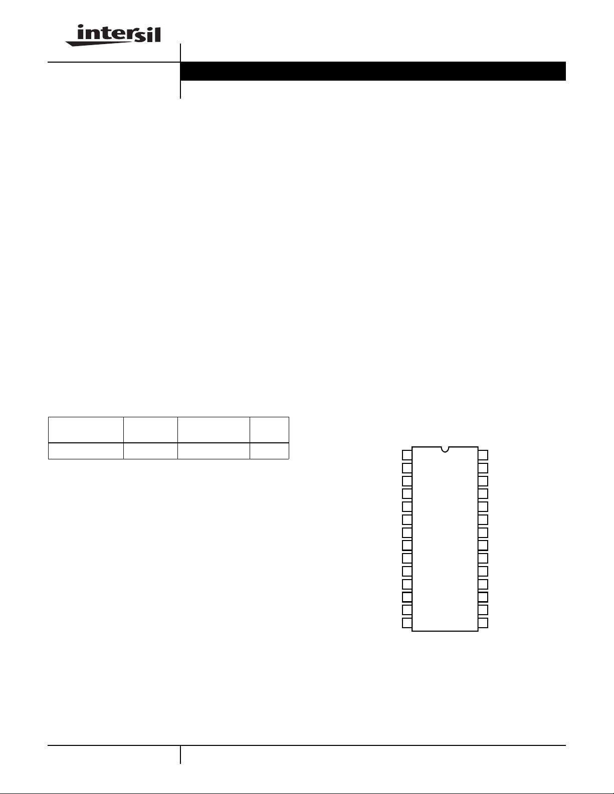
HI-516 (PDIP)
TOP VIEW
1
2
3
4
5
6
7
8
9
10
11
12
13
14
28
27
26
25
24
23
22
21
20
19
18
17
16
15
OUT A
VIN 8/8A
IN 7/7A
IN 6/6A
IN 5/5A
IN 4/4A
IN 3/3A
IN 2/2A
IN 1/1A
ENABLE
A
0
A
1
A
2
1
CAUTION: These devices are sensitive to electrostatic discharge; follow proper IC Handling Procedures.
1-888-INTERSIL or 407-727-9207
| Copyright © Intersil Corporation 1999
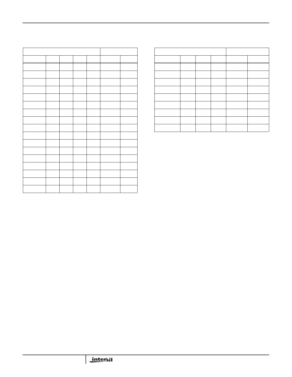
Truth Tables
HI-516 USED AS A 16-CHANNEL MULTIPLEXER OR
DUAL 8-CHANNEL MULTIPLEXER (NOTE 1)
USE A3 AS DIGITAL ADDRESS INPUT ON CHANNEL TO
ENABLE A
L XXXXNone None
H LLLL1A None
H LLLH2A None
H L L H L 3A None
H L L H H 4A None
H L H L L 5A None
H L H L H 6A None
H L H H L 7A None
H LHHH8A None
H H L L L None 1B
H H L L H None 2B
H H L H L None 3B
H H L H H None 4B
H H H L L None 5B
H H H L H None 6B
H HHHLNone 7B
H HHHHNone 8B
NOTE:
1. For 16-channel single-ended function, tie ‘out A’to ‘out B’; for
dual 8-channel function use the A3 address pin to select
between MUX A and MUX B, where MUX A is selected with A
low.
A
A
A
3
2
1
OUT A OUT B
0
HI-516
3
HI-516 USED AS A DIFFERENTIAL 8-CHANNEL MULTIPLEXER
A3 CONNECTED TO V- SUPPLY ON CHANNEL TO
ENABLE A
L X X X None None
H L L L 1A 1B
H L L H 2A 2B
H L H L 3A 3B
H L H H 4A 4B
H H L L 5A 5B
H H L H 6A 6B
H H H L 7A 7B
H H H H 8A 8B
A
2
A
1
OUT A OUT B
0
2
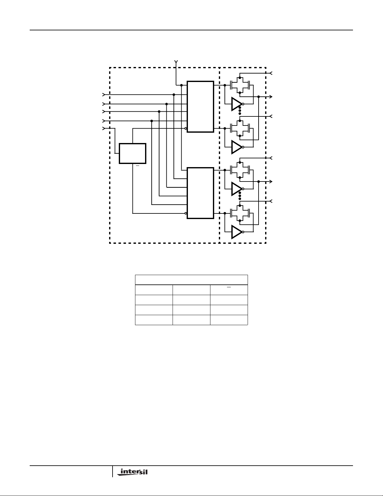
Functional Block Diagram
EN
A
0
A
1
A
2
A
3
Q
A
3
DECODER
Q
HI-516
VDD/LLS
IN 1A
N P
OUT A
DECODER
IN 8A
N P
IN 1B
N P
OUT B
DECODER
IN 8B
INPUT BUFFER AND DECODERS
A3 DECODE
A
3
Q Q
HHL
LLH
V- L L
N P
MULTIPLEXER
SWITCHES
3

HI-516
Absolute Maximum Ratings Thermal Information
V+ to V- . . . . . . . . . . . . . . . . . . . . . . . . . . . . . . . . . . . . . . . . . . . 33V
Analog Signal. . . . . . . . . . . . . . . . . . . . . . . . . . . . . . . . . (VIN,V
OUT
)
. . . . . . . . . . . . . . . . . . . . . . . . . . . . . . . . . . . . . . (V-) -2V to (V+) +2V
Digital Input Voltage:
TTL Levels Selected (VDD/LLS Pin = GND or Open)
V
. . . . . . . . . . . . . . . . . . . . . . . . . . . . . . . . . . . . . . -6V to +6V
A0-2
V
. . . . . . . . . . . . . . . . . . . . . . . . . . . . . (V-) -2V to (V+) +2V
A3/SDS
CMOS Levels Selected (VDD/LLS Pin = VDD)
V
. . . . . . . . . . . . . . . . . . . . . . . . . . . . . . . . . . -2V to (V+) +2V
A0-3
Operating Conditions
Temperature Ranges
HI-516-5 . . . . . . . . . . . . . . . . . . . . . . . . . . . . . . . . . . 0oC to 75oC
CAUTION: Stresses above those listed in “Absolute Maximum Ratings” may cause permanent damage to the device. This is a stress only rating and operation of the
device at these or any other conditions above those indicated in the operational sections of this specification is not implied.
NOTE:
2. θJA is measured with the component mounted on an evaluation PC board in free air.
Thermal Resistance (Typical, Note 2) θJA (oC/W)
PDIP Package . . . . . . . . . . . . . . . . . . . . . . . . . . . . . 60
Maximum Junction Temperature
Plastic Package . . . . . . . . . . . . . . . . . . . . . . . . . . . . . . . . . .150oC
Maximum Storage Temperature Range. . . . . . . . . . -65oC to 150oC
Maximum Lead Temperature (Soldering 10s) . . . . . . . . . . . . .300oC
Electrical Specifications Supplies = +15V, -15V; V
(Logic Level High) = 2.4V, VAL (Logic Level Low) = 0.8V;
AH
VDD/LLS = GND. (Note 3) Unless Otherwise Specified
-5
PARAMETER
TEST
CONDITIONS
TEMP
(oC)
UNITSMIN TYP MAX
DYNAMIC CHARACTERISTICS
Access Time, t
A
25 - 130 175 ns
Full - - 225 ns
Break-Before-Make Delay, t
Enable Delay (ON), t
Enable Delay (OFF), t
ON(EN)
OFF(EN)
OPEN
25 10 20 - ns
25 - 120 175 ns
25 - 140 175 ns
Settling Time To 0.1% 25 - 250 - ns
To 0.01% 25 - 800 - ns
Charge Injection Error Note 6 25 - - 20 mV
Off Isolation Note 7 25 55 - - dB
Channel Input Capacitance, C
Channel Output Capacitance,
C
D(OFF)
Digital Input Capacitance, C
A
Input to Output Capacitance,
C
DS(OFF)
S(OFF)
25 - - 10 pF
25 - - 25 pF
25 - - 10 pF
25 - 0.02 - pF
DIGITAL INPUT CHARACTERISTICS
Input Low Threshold, VAL (TTL) Note 3 Full - - 0.8 V
Input High Threshold, VAH (TTL) Note 3 Full 2.4 - - V
Input Low Threshold, VAL (CMOS) Note 3 Full - - 0.3V
Input High Threshold, VAH (CMOS) Note 3 Full 0.7V
DD
--V
DD
Input Leakage Current, IAH (High) Full - - 1 µA
4
V

HI-516
Electrical Specifications Supplies = +15V, -15V; V
(Logic Level High) = 2.4V, VAL (Logic Level Low) = 0.8V;
AH
VDD/LLS = GND. (Note 3) Unless Otherwise Specified (Continued)
-5
PARAMETER
TEST
CONDITIONS
TEMP
(oC)
UNITSMIN TYP MAX
Input Leakage Current, IAL (Low) Full - - 25 µA
ANALOG CHANNEL CHARACTERISTICS
Analog Signal Range, V
On Resistance, r
ON
IN
Note 4 Full -15 - +15 V
Note 5 25 - 620 750 Ω
Full - - 1,000 Ω
Off Input Leakage Current, l
S(OFF)
25 - 0.01 - nA
Full - - 50 nA
Off Output Leakage Current,
I
D(OFF)
On Channel Leakage Current, I
D(ON)
25 - 0.03 - nA
Full - - 100 nA
25 - 0.04 - nA
POWER SUPPLY CHARACTERISTICS
Power Dissipation, P
D
Full - - 900 mW
I+, Current VEN = 2.4V Full - - 30 mA
I-, Current Full - - 30 mA
NOTES:
3. VDD/LLS pin = open or grounded for TTL compatibility. VDD/LLS pin = VDD for CMOS compatibility.
4. At temperatures above 90oC, care must be taken to assure VIN remains at least 1V below the V
5. VIN = ±10V, I
= -100µA.
OUT
for proper operation.
SUPPLY
6. VIN = 0V, CL = 100pF, enable input pulse = 3V, f = 500kHz.
7. VEN = 0.8V, VIN = 3V
, f = 500kHz, CL = 40pF, RL = 1K, Pin 3 grounded.
RMS
5

HI-516
Test Circuits and Waveforms V
I
100µA
OUT
V
2
IN
OUT
±10V
V
IN
FIGURE 1. ON RESISTANCE TEST CIRCUIT FIGURE 2. I
I
S(OFF)
A
±10V
±
10V
rON =
EN
/LLS = GND, Unless Otherwise Specified.
DD
V
2
100µA
OUT
0.8V
±10V
±
10V
EN
OUT
TEST CIRCUIT (NOTE 8)
D(OFF)
OUT
EN
2.4V
0.8V
I
A
D(OFF)
±
10V
A
I
D(ON)
±10V
FIGURE 3. I
50%
+10V
TEST CIRCUIT (NOTE 8) FIGURE 4. I
S(OFF)
3.5V
ADDRESS
DRIVE (V
10%
t
A
)
A
0V
OUTPUT
-10V
V
A
FIGURE 5A. MEASUREMENT POINTS FIGURE 5B. TEST CIRCUIT
NOTE:
8. Two measurements per channel: ±10V and 10V. (Two measurements per device for I
FIGURE 6. ACCESS TIME
50Ω
2.4V
D(OFF)
TEST CIRCUIT (NOTE 8)
D(ON)
+15V
V+
A3/SDS
2
1
0
IN 2-15
OUT A
OUT B
/LLS
GND
-15V
V
A
A
A
EN
DD
±10V and 10V).
IN 1
IN 16
V-
±10V
±
10V
kΩ
50
10
pF
6

HI-516
Test Circuits and Waveforms V
3.5V
ADDRESS
0V
S1 ON S16 ON
50% 50%
FIGURE 7A. MEASUREMENT POINTS FIGURE 7B. TEST CIRCUIT
3.5V
50%
90%
t
ON(EN)
DRIVE (V
t
OPEN
ENABLE DRIVE (V
50%
10%
t
OFF(EN)
/LLS = GND, Unless Otherwise Specified. (Continued)
DD
)
A
OUTPUT
V
A
50Ω
2.4V
FIGURE 7. BREAK-BEFORE-MAKE DELAY
)
A
0V
OUTPUT
0V
50
V
A
Ω
V
A
A
A
A
EN
DD
3
2
1
0
A
A
A
A
EN
V
DD
/LLS
3
2
1
0
/LLS
GND
+15V
IN 2-15
GND
+15V
V+
IN 1
IN 2-16
OUTA
V-
-15V
V+
IN 1
IN 16
OUTA
OUTB
V-
-15V
800
Ω
800
Ω
+10V
12.5pF
12.5pF
+5V
V
OUT
V
OUT
FIGURE 8A. MEASUREMENT POINTS FIGURE 8B. TEST CIRCUIT
FIGURE 8. ENABLE DELAYS
2.4V
3.0V
V
V
OUT
A
∆V
0V
O
V
A
FIGURE 9A. MEASUREMENT POINTS FIGURE 9B. TEST CIRCUIT
∆VO is the measured voltage error due to charge injection. The error in coulombs is Q = CL x ∆VO.
FIGURE 9. CHARGE INJECTION
7
+15V
V+
A0, A1, A2,
A3/SDS
IN
EN
GND VDD/LLS
OUT
A OR B
V-
-15V
V
OUT
CL = 100pF

Die Characteristics
HI-516
DIE DIMENSIONS:
2250µm x 3720µm x 485µm
METALLIZATION:
Type: CuAl
Thickness: 16k
Å ±2kÅ
Metallization Mask Layout
IN 1/1A (19)
IN 2/2A (20)
ENABLE
(18)
HI-516
A
0
(17)
PASSIVATION:
Type: Nitride Over Silox
Nitride Thickness: 3.5k
Å ±1kÅ
Silox Thickness: 12kű2kÅ
WORST CASE CURRENT DENSITY:
5
2
A
(16)
1
1.64 x 10
A
A
2
(15)
/SDS
3
(14)
A/cm
V
DD
(13)
/LLS
GND
(12)
(10) IN 9/1B
(9) IN 10/2B
IN 3/3A (21)
IN 4/4A (22)
IN 5/5A (23)
IN 6/6A (24)
IN 7/7A (25)
IN 8/8A (26)
(27)
-V
(28)
OUT A
(8) IN 11/3B
(7) IN 12/4B
(6) IN 13/5B
(5) IN 14/6B
(4) IN 15/7B
(3) IN 16/8B
(1)+V(2)
OUT B
All Intersil semiconductor products are manufactured, assembled and tested under ISO9000 quality systems certification.
Intersil semiconductor products are sold by description only.Intersil Corporation reserves the right to make changes in circuit design and/or specifications at any time without notice. Accordingly, the reader is cautioned to verify that data sheets are current before placing orders. Information furnished by Intersil is believed to be accurate and
reliable. Howev er, no responsibility is assumed by Intersil or its subsidiaries for its use; nor foranyinfringements of patents or other rights of third parties which may result
from its use. No license is granted by implication or otherwise under any patent or patent rights of Intersil or its subsidiaries.
For information regarding Intersil Corporation and its products, see web site http://www.intersil.com
8
 Loading...