HI-506A, HI-507A, HI-508A, HI-509A
Data Sheet June 1999
16-Channel, 8-Channel, Differential
8-Channel and Differential 4-Channel,
CMOS Analog MUXs with Active
Overvoltage Protection
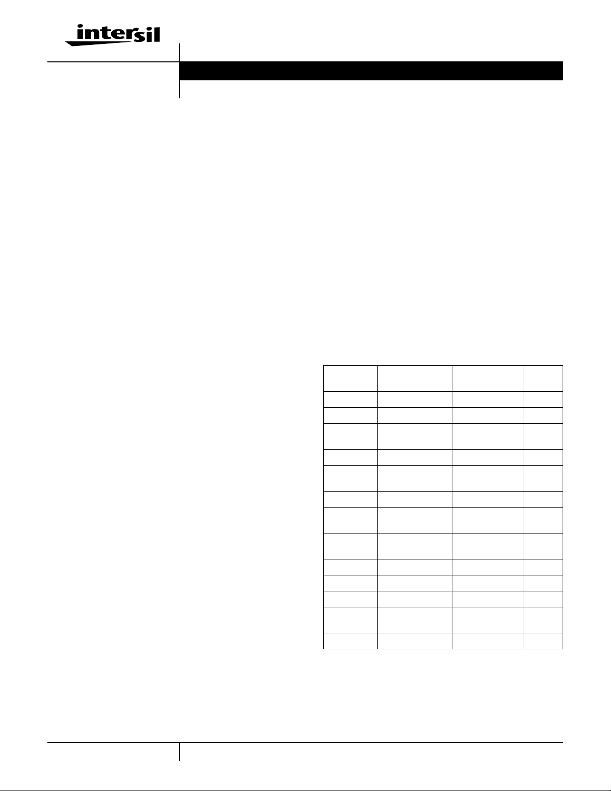
The HI-506A, HI-507A, HI-508A and HI-509A are analog
multiplexers with active overvoltage protection. Analog input
levels may greatly exceed either power supply without
damaging the device or disturbing the signal path of other
channels. Active protection circuitry assures that signal
fidelity is maintained even under fault conditions that would
destroy other multiplexers. Analog inputs can withstand
constant 70V
also sustain continuous faults up to 4V greater than either
supply. In addition, signal sources are protected from short
circuiting should multiplexer supply loss occur. Each input
presents 1kΩ of resistance under this condition. These
features make the HI-506A, HI-507A, HI-508A and HI-509A
ideal for use in systems where the analog inputs originate
from external equipment, or separately powered circuitry. All
devices are fabricated with 44V dielectrically isolated CMOS
technology. The HI-506A is a single 16-Channel multiplexer,
the HI-507A is an 8-Channel differential multiplexer, the
HI-508A isasingle8-Channelmultiplexer andtheHI-509Ais
a differential 4-Channel multiplexer. If input overvoltage
protection is not needed the HI-506/507/508/509
multiplexers are recommended. For further information see
Application Notes AN520 and AN521.
levelswith±15Vsupplies.Digitalinputswill
P-P
File Number 3143.2
Features
• Analog Overvoltage . . . . . . . . . . . . . . . . . . . . . . . .70V
• No Channel Interaction During Overvoltage
• Maximum Power Supply. . . . . . . . . . . . . . . . . . . . . . . 44V
• Fail Safe with Power Loss (No Latch-Up)
• Break-Before-Make Switching
• Analog Signal Range . . . . . . . . . . . . . . . . . . . . . . . . ±15V
• Access Time. . . . . . . . . . . . . . . . . . . . . . . . . . . . . . .500ns
• Power Dissipation . . . . . . . . . . . . . . . . . . . . . . . . . 7.5mW
P-P
Applications
• Data Acquisition Systems
• Industrial Controls
• Telemetry
Ordering Information
PART
NUMBER
HI1-0506A-2 -55 to 125 28 Ld CERDIP F28.6
HI1-0506A-5 0 to 75 28 Ld CERDIP F28.6
HI1-0506A-8 -55 to 125
HI3-0506A-5 0 to 75 28 Ld PDIP E28.6
HI1-0507A-8 -55 to 125
HI3-0507A-5 0 to 75 28 Ld PDIP E28.6
HI1-0508A-7 0 to 75
HI1-0508A-8 -55 to 125
HI3-0508A-5 +0 to 75 16 Ld PDIP E16.3
HI1-0509A-2 -55 to 125 16 Ld CERDIP F16.3
HI1-0509A-5 0 to 75 16 Ld CERDIP F16.3
HI1-0509A-8 -55 to 125
HI3-0509A-5 0 to 75 16 Ld PDIP E16.3
TEMP. RANGE
(oC) PACKAGE
+ 160 Hour Burn-In
+ 160 Hour Burn-In
+ 96 Hour Burn-In
+ 160 Hour Burn-In
+ 160 Hour Burn-In
PKG.
NO.
28 Ld CERDIP F28.6
28 Ld CERDIP F28.6
16 Ld CERDIP F16.3
16 Ld CERDIP F16.3
16 Ld CERDIP F16.3
1
CAUTION: These devices are sensitive to electrostatic discharge; follow proper IC Handling Procedures.
1-888-INTERSIL or 321-724-7143
| Copyright © Intersil Corporation 1999

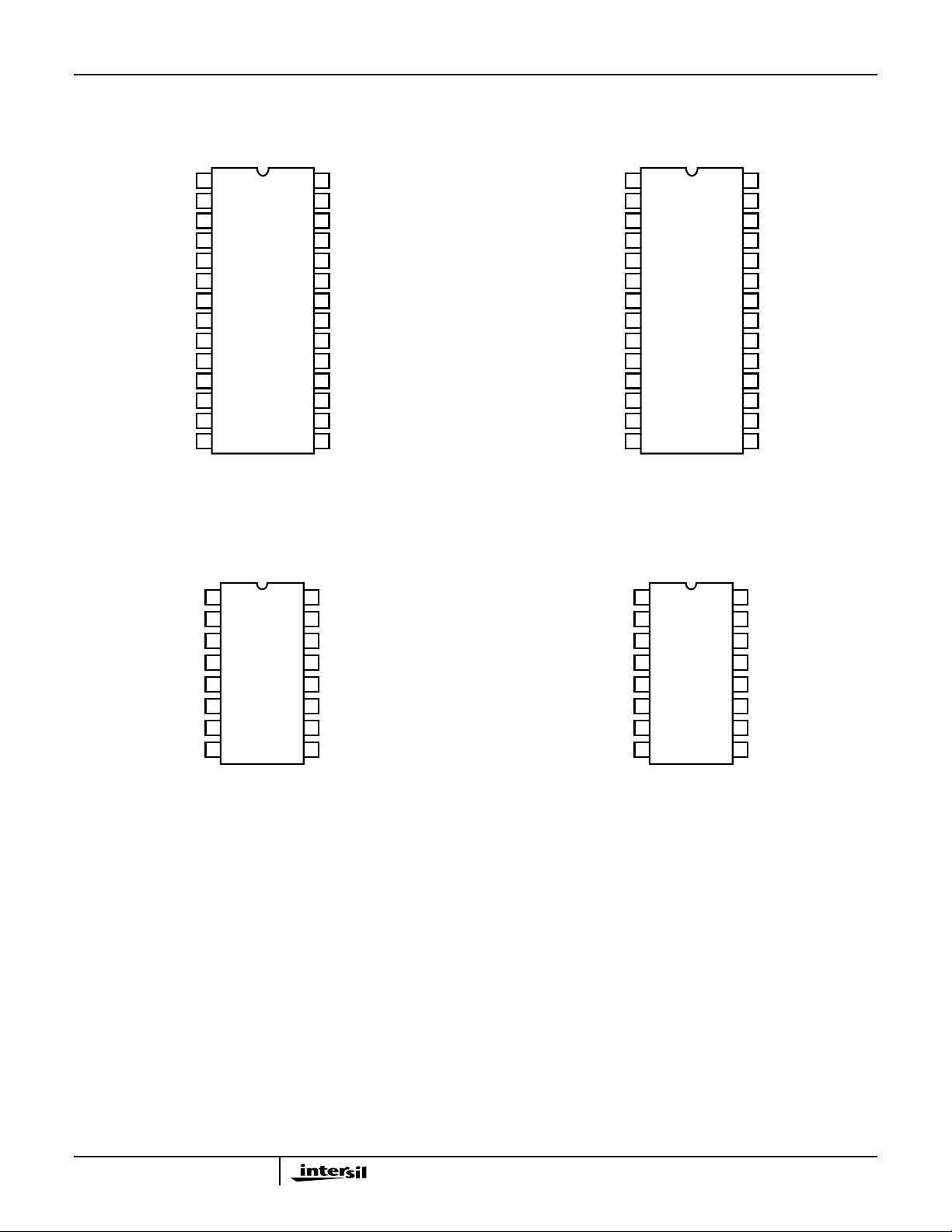
Pinouts
HI-506A (CERDIP, PDIP)
TOP VIEW
HI-506A, HI-507A, HI-508A, HI-509A
HI-507A (CERDIP, PDIP)
TOP VIEW
+V
SUPPLY
IN 16
IN 15
IN 14
IN 13
IN 12
IN 11
IN 10
IN 9
GND
V
REF
ADDRESS A
ENABLE
-V
SUPPLY
1
NC
2
3
NC
4
5
6
7
8
9
10
11
12
13
14
3
HI-508A (CERDIP, PDIP)
TOP VIEW
1
A
0
2
3
4
IN 1
5
IN 2
6
IN 3
7
IN 4
8
OUT
28
27
26
25
24
23
22
21
20
19
18
17
16
15
16
A
15
A
14
GND
13
+V
12
IN 5
IN 6
11
10
IN 7
9
IN 8
OUT
-V
SUPPLY
IN 8
IN 7
IN 6
IN 5
IN 4
IN 3
IN 2
IN 1
ENABLE
ADDRESS A
ADDRESS A
ADDRESS A
1
2
SUPPLY
28
+V
SUPPLY
0
1
2
OUT B
NC
IN 8B
IN 7B
IN 6B
IN 5B
IN 4B
IN 3B
IN 2B
IN 1B
GND
V
REF
NC
1
2
3
4
5
6
7
8
9
10
11
12
13
14
OUT A
-V
27
SUPPLY
26
IN 8A
25
IN 7A
IN 6A
24
IN 5A
23
IN 4A
22
IN 3A
21
20
IN 2A
IN 1A
19
ENABLE
18
17
ADDRESS A
16
ADDRESS A
ADDRESS A
15
0
1
2
HI-509A (CERDIP, PDIP)
TOP VIEW
16
ENABLE
-V
SUPPLY
IN 1A
IN 2A
IN 3A
IN 4A
OUT A
1
A
0
2
3
4
5
6
7
8
15
14
13
12
11
10
9
A
1
GND
+V
SUPPLY
IN 1B
IN 2B
IN 3B
IN 4B
OUT B
2

HI-506A, HI-507A, HI-508A, HI-509A
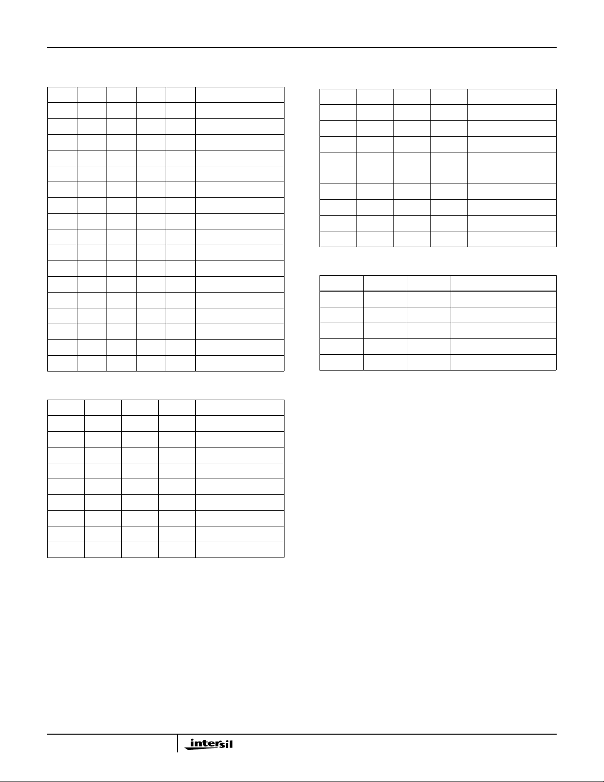
Truth Tables
HI-506A
A
A
3
A
2
XXXXL None
LLLLH 1
LLLHH 2
LLHLH 3
LLHHH 4
LHLLH 5
LHLHH 6
LHHLH 7
LHHHH 8
HLLLH 9
HLLHH 10
HLHLH 11
HLHHH 12
HHLLH 13
HHLHH 14
HHHLH 15
HHHHH 16
A
1
EN “ON” CHANNEL
0
HI-508A
A
2
A
1
A
0
EN “ON” CHANNEL
X X X L None
LLLH 1
LLHH 2
LHLH 3
LHHH 4
HLLH 5
HLHH 6
HHLH 7
HHHH 8
HI-509A
A
1
A
0
EN “ON” CHANNEL PAIR
X X L None
LLH 1
LHH 2
HLH 3
HHH 4
HI-507A
A
2
A
1
A
0
EN “ON” CHANNEL PAIR
X X X L None
LLLH 1
LLHH 2
LHLH 3
LHHH 4
HLLH 5
HLHH 6
HHLH 7
HHHH 8
3

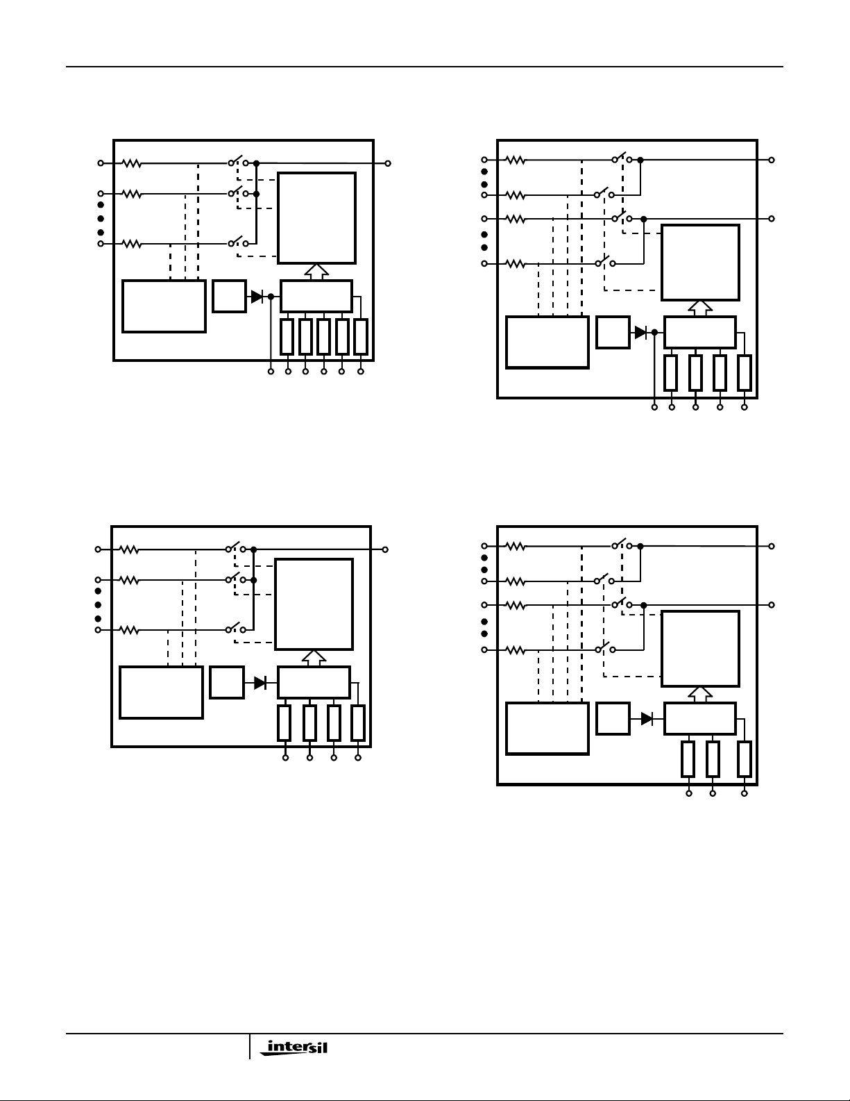
Functional Diagrams
HI-506A HI-507A
HI-506A, HI-507A, HI-508A, HI-509A
IN 1
IN 2
IN 16
IN 1
IN 2
IN 8
1K
1K
1K
OVERVOLTAGE
CLAMP AND
SIGNAL
ISOLATION
† DIGITAL INPUT
PROTECTION
1K
1K
1K
1K
1K
1K
1K
OVERVOLTAGE
CLAMP AND
SIGNAL
ISOLATION
† DIGITAL INPUT
PROTECTION
5V
REF
5V
REF
V
REF
DECODER/
DRIVER
LEVEL
SHIFT
† † † †
A
0A1A2A3
EN
OUT
IN 1A
IN 8A
IN 1B
IN 8B
†
HI-508A HI-509A
1K
1K
1K
1K
DECODER/
DRIVER
OUT
IN 1A
IN 4A
IN 1B
IN 4B
V
REF
DECODER/
DRIVER
LEVEL
SHIFT
† † †
A0A1A
DECODER/
DRIVER
OUT
A
OUT
B
†
EN
2
OUT
A
OUT
B
OVERVOLTAGE
CLAMP AND
SIGNAL
ISOLATION
† DIGITAL INPUT
PROTECTION
5V
REF
LEVEL
SHIFT
† † †
A
0A1A2
EN
OVERVOLTAGE
†
CLAMP AND
SIGNAL
ISOLATION
† DIGITAL INPUT
PROTECTION
5V
REF
LEVEL
SHIFT
† †
A
0A1
†
EN
4

Schematic Diagrams
V
REF
HI-506A, HI-507A, HI-508A, HI-509A
TTL REFERENCE
CIRCUIT
V+
R10
R9
Q1
Q4
D3
GND
ADDRESS INPUT BUFFER AND LEVEL SHIFTER
LEVEL SHIFTER
V+
OVERVOLTAGE
PROTECTION
V+
D2
R1
D1
200
Ω
V-
ADD
IN
P
P
N
N
P
P
R2
R3
N
N
R4
GND
P
N
P P
N
P
R5 R7
R6
N
R8
N
P
N
V-
P
LEVEL
SHIFTED
ADDRESS
TO
DECODE
N
ADDRESS DECODER
V+
P
PP PP P P
TO P-CHANNEL
DEVICE OF
THE SWITCH
A
OR A
0
N
0
N
NN
ENABLE
5
A2 OR A
A3 OR A
3
DELETE A
FOR HI-507A, HI-508A, HI-509A
DELETE A
3
2
A1 OR A
1
2
OR A3INPUT
OR A2 INPUT FOR HI-509A
N
N
N
TO N-CHANNEL
DEVICE OF
THE SWITCH
V-

HI-506A, HI-507A, HI-508A, HI-509A
Schematic Diagrams (Continued)
FROM DECODE
OVERVOLTAGE PROTECTION
MULTIPLEX SWITCH
V+
P
Q5
N
IN
FROM DECODE
R11
1K
D6
D7 D4 D5
Q6
N
OUT
N
V-
P
6

HI-506A, HI-507A, HI-508A, HI-509A
Absolute Maximum Ratings Thermal Information
V+ to V- . . . . . . . . . . . . . . . . . . . . . . . . . . . . . . . . . . . . . . . . . . +44V
V+ to GND . . . . . . . . . . . . . . . . . . . . . . . . . . . . . . . . . . . . . . . . +22V
V- to GND. . . . . . . . . . . . . . . . . . . . . . . . . . . . . . . . . . . . . . . . . .-25V
Digital Input Voltage (VEN, VA) . . . . . . . . . . . . . (V-) -4V to (V+) +4V
or 20mA, Whichever Occurs First
Analog Signal (VIN, V
). . . . . . . . . . . . . . . (V-) -20V to (V+) +20V
OUT
Continuous Current, IN or OUT . . . . . . . . . . . . . . . . . . . . . . . . 20mA
Peak Current, IN or OUT, Pulsed 1ms, 10% Duty Cycle (Max). . 40mA
Operating Conditions
Temperature Ranges
HI-506A/507A/508A/509A-2, -8 . . . . . . . . . . . . . . -55oC to 125oC
HI-506A/507A/508A/509A-5, -7 . . . . . . . . . . . . . . . . .0oC to 75oC
CAUTION: Stresses above those listed in “Absolute Maximum Ratings” may cause permanent damage to the device. This is a stress only rating and operation of the
device at these or any other conditions above those indicated in the operational sections of this specification is not implied.
NOTE:
1. θJA is measured with the component mounted on an evaluation PC board in free air.
Thermal Resistance (Typical, Note 1) θJA (oC/W) θJC (oC/W)
28 Ld CERDIP Package. . . . . . . . . . . . 55 18
16 Ld CERDIP Package. . . . . . . . . . . . 85 32
28 Ld PDIP Package . . . . . . . . . . . . . . 60 N/A
16 Ld PDIP Package . . . . . . . . . . . . . . 90 N/A
Maximum Junction Temperature
CERDIP Packages. . . . . . . . . . . . . . . . . . . . . . . . . . . . . . . .175oC
PDIP Packages . . . . . . . . . . . . . . . . . . . . . . . . . . . . . . . . . .150oC
Maximum Storage Temperature Range. . . . . . . . . . -65oC to 150oC
Maximum Lead Temperature (Soldering 10s) . . . . . . . . . . . . .300oC
Electrical Specifications Supplies = +15V, -15V; V
Pin = Open; VAH (Logic Level High) = 4V; VAL (Logic Level Low) = 0.8V,
REF
Unless Otherwise Specified. For Test Conditions, Consult Test Circuits Section
-2, -8 -5, -7
UNITSMIN TYP MAX MIN TYP MAX
PARAMETER
TEST
CONDITIONS
TEMP
(oC)
DYNAMIC CHARACTERISTICS
Access Time, t
A
Note 2 25 - 0.5 - - 0.5 - µs
Full - - 1.0 - - 1.0 µs
Break-Before-Make Delay, t
Enable Delay (ON), t
ON(EN)
OPEN
Note 2 25 25 80 - 25 80 - ns
Note 2 25 - 300 500 - 300 - ns
Full - - 1000 - - 1000 ns
Enable Delay (OFF), t
OFF(EN)
Note 2 25 - 300 500 - 300 - ns
Full - - 1000 - - 1000 ns
Settling Time, t
S
HI-506A and HI-507A To 0.1% 25 - 1.2 - - 1.2 - µs
To 0.01% 25 - 3.5 - - 3.5 - µs
HI-508A and HI-509A To 0.1% 25 - 1.2 - - 1.2 - µs
To 0.01% 25 - 3.5 - - 3.5 - µs
Off Isolation Note 7 25 50 68 - 50 68 - dB
Channel Input Capacitance, C
Channel Output Capacitance, C
S(OFF)
D(OFF)
25 -10- -10-pF
HI-506A 25 - 52 - - 52 - pF
HI-507A 25 - 30 - - 30 - pF
HI-508A 25 - 25 - - 25 - pF
HI-509A 25 - 12 - - 12 - pF
Digital Input Capacitance, C
A
Input to Output Capacitance, C
DS(OFF)
25 -10- -10-pF
25 - 0.1 - - 0.1 - pF
DIGITAL INPUT CHARACTERISTICS
Input Low Threshold, TTL Drive, V
Input High Threshold, V
AH
AL
(Note 9) Note 2 Full 4.0 - - 4.0 - - V
Input Leakage Current (High or Low), I
A
Note 2 Full - - 0.8 - - 0.8 V
Notes 2, 6 Full - - 1.0 - - 1.0 µA
7

HI-506A, HI-507A, HI-508A, HI-509A
Electrical Specifications Supplies = +15V, -15V; V
Pin = Open; VAH (Logic Level High) = 4V; VAL (Logic Level Low) = 0.8V,
REF
Unless Otherwise Specified. For Test Conditions, Consult Test Circuits Section (Continued)
-2, -8 -5, -7
UNITSMIN TYP MAX MIN TYP MAX
PARAMETER
MOS Drive, VAL, HI-506A/HI-507A V
MOS Drive, V
, HI-506A/HI-507A V
AH
TEST
CONDITIONS
= +10V 25 - - 0.8 - - 0.8 V
REF
= +10V 25 6.0 - - 6.0 - - V
REF
TEMP
(oC)
ANALOG CHANNEL CHARACTERISTICS
Analog Signal Range, V
On Resistance, r
ON
IN
Note 2 Full -15 - +15 -15 - +15 V
Notes 2, 3 25 - 1.2 1.5 - 1.5 1.8 kΩ
Full - 1.5 1.8 - 1.8 2.0 kΩ
Off Input Leakage Current, I
S(OFF)
Notes 2, 4 25 - 0.03 - - 0.03 - nA
Full - - 50 - - 50 nA
Off Output Leakage Current, I
D(OFF)
Notes 2, 4 25 - 0.1 - - 0.1 - nA
HI-506A Full - - 300 - - 300 nA
HI-507A Full - - 200 - - 200 nA
HI-508A Full - - 200 - - 200 nA
HI-509A Full - - 100 - - 100 nA
I
With Input Overvoltage Applied Note 5 25 - 4.0 - - 4.0 - nA
D(OFF)
Full - - 2.0 - - - µA
On Channel Leakage Current, I
D(ON)
Notes 2, 4 25 - 0.1 - - 0.1 - nA
HI-506A Full - - 300 - - 300 nA
HI-507A Full - - 200 - - 200 nA
HI-508A Full - - 200 - - 200 nA
HI-509A Full - - 100 - - 100 nA
Differential Off Output Leakage Current, I
DIFF
,
Full - - 50 - - 50 nA
(HI-507A, HI-509A Only)
POWER SUPPLY CHARACTERISTICS
Current, I+ Notes 2, 8 Full - 0.5 2.0 - 0.5 2.0 mA
Current, I- Notes 2, 8 Full - 0.02 1.0 - 0.02 1.0 mA
Power Dissipation, P
D
Full - 7.5 - - 7.5 - mW
NOTES:
o
2. 100% tested for Dash 8. Leakage currents not tested at -55
3. V
OUT
= ±10V, I
= +100µA.
OUT
C.
4. 10nA is the practical lower limit for high speed measurement in the production test environment.
5. Analog Overvoltage = ±33V.
6. Digital input leakage is primarily due to the clamp diodes (see Schematic). Typical leakage is less than 1nA at 25oC.
7. VEN = 0.8V, RL = 1K, CL = 15pF, VS = 7V
, f = 100kHz.
RMS
8. VEN, VA = 0V or 4V.
9. To drive from DTL/TTL Circuits, 1kΩ pull-up resistors to +5V supply are recommended.
8

HI-506A, HI-507A, HI-508A, HI-509A
T est Cir cuits and Waveforms T
1.4
1.3
1.2
1.1
1.0
0.9
0.8
ON RESISTANCE (kΩ)
0.7
0.6
-10
-8 246810-6 -4 -2 0
125oC
25oC
-55oC
ANALOG INPUT (V)
= 25oC, V
A
= ±15V, VAH = 4V, VAL = 0.8V, V
SUPPLY
Unless Otherwise Specified
100µA
V
2
V
IN
FIGURE 1A. TEST CIRCUIT
NORMALIZED RESISTANCE
(REFERRED TO VALUE AT ±15V)
OUTIN
rON =
1.5
1.4
1.3
1.2
1.1
1.0
0.9
0.8
56
= Open,
REF
V
2
100µA
-55oC TO 125oC
V
= +5V
IN
7 8 9 10 11 12 13 14 15
SUPPLY VOLTAGE (±V)
FIGURE 1B. ON RESISTANCE vs ANALOG INPUT VOLTAGE FIGURE 1C. NORMALIZED ON RESISTANCE vsSUPPLY
VOLTAGE
FIGURE 1. ON RESISTANCE
100nA
10nA
OFF OUTPUT
ON LEAKAGE
CURRENT
I
1nA
LEAKAGE CURRENT
100pA
10pA
25 50 75 100 125
D(ON)
CURRENT
I
D(OFF)
OFF INPUT
LEAKAGE CURRENT
I
S(OFF)
TEMPERATURE (
±10V
o
C)
FIGURE 2A. LEAKAGE CURRENT vs TEMPERATURE FIGURE 2B. I
TEST CIRCUIT (NOTE 10)
D(OFF)
EN
OUT
A
+0.8V
I
D(OFF)
±
10V
9

HI-506A, HI-507A, HI-508A, HI-509A
T est Cir cuits and Waveforms T
= 25oC, V
A
= ±15V, VAH = 4V, VAL = 0.8V, V
SUPPLY
Unless Otherwise Specified (Continued)
OUT
I
A
S(OFF)
±10V
FIGURE 2C. I
±
10V
TEST CIRCUIT (NOTE 10) FIGURE 2D. I
S(OFF)
EN
+0.8V
±
10V
NOTE:
10. Two measurements per channel: ±10V and +10V. (Two measurements per device for I
FIGURE 2. LEAKAGE CURRENTS
7
18
ANALOG INPUT
15
12
CURRENT (I
)
IN
6
5
4
D(OFF)
= Open,
REF
A
0
D(On)
A
1
TEST CIRCUIT (NOTE 10)
±10V and +10V.)
EN
OUT
4V
A
I
D(ON)
±10V
9
6
3
ANALOG INPUT CURRENT (mA)
0
15 18 21 24 27 30 33 36
ANALOG INPUT OVERVOLTAGE (±V)
OUTPUT OFF LEAKAGE
CURRENT ID
(OFF)
FIGURE 3A. ANALOG INPUTOVERVOLTAGE
CHARACTERISTICS
FIGURE 3. ANALOG INPUT OVERVOLTAGE CHARACTERISTICS
±14
±12
±10
±8
±6
±4
SWITCH CURRENT (mA)
±2
-55oC
3
2
1
0
25oC
125oC
OUTPUT OFF LEAKAGE CURRENT (nA)
I
A
IN
±V
IN
I
A
D(OFF)
FIGURE 3B. TEST CIRCUIT
±V
IN
A
0
2 4 6 8 10 12 14
0
VOLTAGE ACROSS SWITCH (±V)
FIGURE 4A. ON CHANNEL CURRENT vs VOLTAGE FIGURE 4B. TEST CIRCUIT
FIGURE 4. ON CHANNEL CURRENT
10

HI-506A, HI-507A, HI-508A, HI-509A
T est Cir cuits and Waveforms T
= 25oC, V
A
= ±15V, VAH = 4V, VAL = 0.8V, V
SUPPLY
REF
= Open,
Unless Otherwise Specified (Continued)
8
6
4
2
SUPPLY CURRENT (mA)
0
1K
V
= ±15V
SUPPLY
V
= ±10V
SUPPLY
10K 100K 1M 10M
TOGGLE FREQUENCY (Hz)
A
3
HI-506A
A
2
50Ω
V
A
+4V
A
A
EN
1
0
GND
+15V/+10V
A
V+
IN 1
†
IN 2
THRU
IN 7/IN 15
IN 8/IN 16
OUT
V-
A
-15V/-10V
+I
SUPPLY
-I
SUPPLY
FIGURE 5A. SUPPLY CURRENT vs TOGGLE FREQUENCY †Similar connection for HI-507A/HI-508A/HI-509A
FIGURE 5B. TEST CIRCUIT
FIGURE 5. DYNAMIC SUPPLY CURRENT
V+
IN 2 THRU
IN 7/IN 15
HI-506A
IN 16
OUT
V-
+15V
IN 1
†
-15V
900
V
REF
V
800
700
600
500
ACCESS TIME (ns)
400
300
REF
3
468101214
= OPEN FOR LOGIC HIGH LEVEL ≤ 6V
= LOGIC HIGH FOR LOGIC HIGH LEVELS > 6V
579 151311
LOGIC LEVEL (HIGH) (V)
V
REF
A
3
A
2
50Ω
V
A
+4V
A
A
EN
1
0
GND
FIGURE 6A. ACCESS TIME vs LOGIC LEVEL (HIGH) †Similar connection for HI-507A/HI-580A/HI-509A
FIGURE 6B. TEST CIRCUIT
±
10V
±10V/±5V
10V/±5V
10
MΩ
±10V
10
kΩ
±
14
pF
50
pF
VA INPUT
2V/DIV.
S1 ON
S16 ON
200ns/DIV.
OUTPUT
5V/DIV.
1
/2 V
+10V
AH
VAH = 4.0V
t
A
10%
ADDRESS
DRIVE (V
OUTPUT
-10V
)
A
0V
FIGURE 6C. MEASUREMENT POINTS FIGURE 6D. WAVEFORMS
FIGURE 6. ACCESS TIME
11

HI-506A, HI-507A, HI-508A, HI-509A
T est Cir cuits and Waveforms T
A
3
HI-506A†
A
2
50Ω
V
A
+4.0V
A
A
EN
1
0
GND
†Similar connection for HI-507A/HI-508A/HI-509A
FIGURE 7A. TEST CIRCUIT FIGURE 7B. MEASUREMENT POINTS
IN 1
IN 2 THRU
IN 7/IN 15
IN 8/IN 16
OUT
1kΩ
= 25oC, V
A
= ±15V, VAH = 4V, VAL = 0.8V, V
SUPPLY
Unless Otherwise Specified (Continued)
+5V
V
OUT
50pF
0V
= Open,
REF
VAH = 4.0V
50% 50%
t
OPEN
ADDRESS
DRIVE (V
)
A
OUTPUT
VA INPUT
2V/DIV.
S1 ON S16 ON
OUTPUT
0.5V/DIV.
100ns/DIV.
FIGURE 7C. WAVEFORMS
FIGURE 7. BREAK-BEFORE-MAKE DELAY
12

HI-506A, HI-507A, HI-508A, HI-509A
T est Cir cuits and Waveforms T
A
3
A
2
A
1
A
0
EN
V
A
50Ω
GND
†Similar connection for HI-507A//HI-508A/HI-509A
FIGURE 8A. TEST CIRCUIT FIGURE 8B. MEASUREMENT POINTS
HI-506A
IN 2 THRU
IN 7/IN 15
IN 8 /IN 16
†
IN 1
OUT
1kΩ
= 25oC, V
A
= ±15V, VAH = 4V, VAL = 0.8V, V
SUPPLY
Unless Otherwise Specified (Continued)
+10V
V
OUT
50pF
50%
VAH = 4.0V
90%
t
ON(EN)
REF
= Open,
50%
t
OFF(EN)
ENABLE DRIVE
)
(V
A
0V
OUTPUT
10%
0V
ENABLE DRIVE
2V/DIV.
DISABLED
ENABLED
ON)
(S
1
100ns/DIV.
FIGURE 8C. WAVEFORMS
FIGURE 8. ENABLE DELAYS
OUTPUT
2V/DIV.
13

Die Characteristics
HI-506A, HI-507A, HI-508A, HI-509A
DIE DIMENSIONS:
159 mils x 83.9 mils
METALLIZATION:
Type: CuAl
Thickness: 16k
Å ±2kÅ
SUBSTRATE POTENTIAL (NOTE):
-V
SUPPLY
PASSIVATION:
Silox: 12k
Å ±2kÅ
Nitride: 3.5kÅ ±1kÅ
NOTE: The substrate appears resistiveto the -V
conductor at -V
SUPPLY
potential.
Metallization Mask Layouts
HI-506A HI-507A
EN
(18) (17) (16) (15) (13) (12)
A
0
A
A
2
1
A
(14)
V
REF
3
WORST CASE CURRENT DENSITY:
5
2
1.4 x 10
A/cm
TRANSISTOR COUNT:
485
PROCESS:
CMOS-DI
terminal, therefore it maybe left floating (Insulating Die Mount) or it may be mounted on a
SUPPLY
NC
GND
EN
(18) (17) (16) (15)
A
0
A
A
1
2
V
REF
(14)
(13) (12)
GND
IN 1
(19)
IN 2
(20)
IN 3
(21)
IN 4
(22)
IN 5
(23)
IN 6
(24)
IN 7
(25)
IN 8
(26)
V- (27) +V (1) NC (2)
OUT (28)
IN 9
(11)
IN 10
(10)
IN 11
(9)
IN 12
(8)
IN 13
(7)
IN 14
(6)
IN 15
(5)
IN 16
(4)
IN 1A
(19)
IN 2A
(20)
IN 3A
(21)
IN 4A
(22)
IN 5A
(23)
IN 6A
(24)
IN 7A
(25)
IN 8A
(26)
V- (27) +V (1) OUT B(2)
OUT A (28)
IN 1B
(11)
IN 2B
(10)
IN 3B
(9)
IN 4B
(8)
IN 5B
(7)
IN 6B
(6)
IN 7B
(5)
IN 8B
(4)
14

Die Characteristics
HI-506A, HI-507A, HI-508A, HI-509A
DIE DIMENSIONS:
108 mils x 83 mils
METALLIZATION:
Type: CuAl
Thickness: 16k
Å ±2kÅ
SUBSTRATE POTENTIAL (NOTE):
-V
SUPPLY
PASSIVATION:
Silox: 12k
Å ±2kÅ
Nitride: 3.5kÅ ±1kÅ
NOTE: The substrate appears resistive to the -V
conductor at -V
SUPPLY
potential.
Metallization Mask Layouts
HI-508A HI-509A
IN 6 IN 7 IN 8 OUT IN 4 IN 3
(11) (10) (9) (8) (7) (6)
WORST CASE CURRENT DENSITY:
5
2
1.4 x 10
A/cm
TRANSISTOR COUNT:
253
PROCESS:
CMOS-DI
terminal, therefore it may be left floating (Insulating Die Mount) or it may be mounted on a
SUPPLY
IN 3B IN 4B OUT B OUT A IN 4AIN 3A
(11) (10) (9) (8) (7) (6)
IN 5
(12)
+V
(13)
GND
(14)
A
2
(15) (16) (1)
A
A
1
IN 2
(5)
IN 1
(4)
-V
(3)
EN
0
(2)
IN 2B
(12)
IN 1B
(13)
+V
(14)
GND
(15) (16) (1)
A
1
A
EN
0
(2)
IN 2A
(5)
IN 1A
(4)
-V
(3)
All Intersil semiconductor products are manufactured, assembled and tested under ISO9000 quality systems certification.
Intersil semiconductor products are sold by description only. Intersil Corporation reserves the right to make changes in circuit design and/or specifications at any time without notice. Accordingly, the reader is cautioned to verify that data sheets are current before placing orders. Information furnished by Intersil is believed to be accurate and
reliable. However,no responsibility is assumed by Intersil or its subsidiaries for its use; nor for any infringements of patents or other rights of third parties which may result
from its use. No license is granted by implication or otherwise under any patent or patent rights of Intersil or its subsidiaries.
For information regarding Intersil Corporation and its products, see web site www.intersil.com
15
 Loading...