


SEMICONDUCTOR
http://www.BDTIC.com/Intersil
www.BDTIC.com/Intersil
HI-5040 thru HI-5051,
HI-5046A and HI-5047A
August 1997
Features
• Wide Analog Signal Range . . . . . . . . . . . . . . . . . . ±15V
• Low “ON” Resistance (Typ) . . . . . . . . . . . . . . . . . . 25Ω
• High Current Capability (Typ). . . . . . . . . . . . . . . . 80mA
• Break-Before-Make Switching
- Turn-On Time (Typ) . . . . . . . . . . . . . . . . . . . . . . 370ns
- Turn-Off Time (Typ) . . . . . . . . . . . . . . . . . . . . . 280ns
• No Latch-Up
• Input MOS Gates are Protected from Electrostatic
Discharge
• DTL, TTL, CMOS, PMOS Compatible
Applications
• High Frequency Switching
• Sample and Hold
• Digital Filters
• Operational Amplifier Gain Switching
CMOS Analog Switches
Description
This family of CMOS analog switches offers low resistance
switching performance for analog voltages up to the supply
rails and for signal currents up to 80mA. “ON” resistance is
low and stays reasonably constant over the full range of
operating signal voltage and current. r
exceptionally constant for input voltages between +5V and
-5V and currents up to 50mA. Switch impedance also
changes very little over temperature, particularly between
o
0
C and 75oC. rON is nominally 25Ω for HI-5048 through
HI-5051 and HI-5046A and HI-5047A and 50Ω for HI-5040
through HI-5047.
All devices provide break-before-make switching and are
TTL and CMOS compatible for maximum application
versatility. Performance is further enhanced by Dielectric
Isolation processing which insures latch-free operation with
very low input and output leakage currents (0.8nA at 25
This family of switches also features very low power
operation (1.5mW at 25
There are 14 devices in this switch series which are
differentiated by type of switch action and value of R
Functional Description). All devices are available in 16 lead
DIP packages. The HI-5040 and HI-5050 switches can
directly replace IH-5040 series devices except IH5048, and
are functionally compatible with the DG180 and DG190
family. Each switch type is available in the -55
o
and 0
C to 75oC performance grades.
o
C).
remains
ON
ON
o
C to 125oC
o
C).
(see
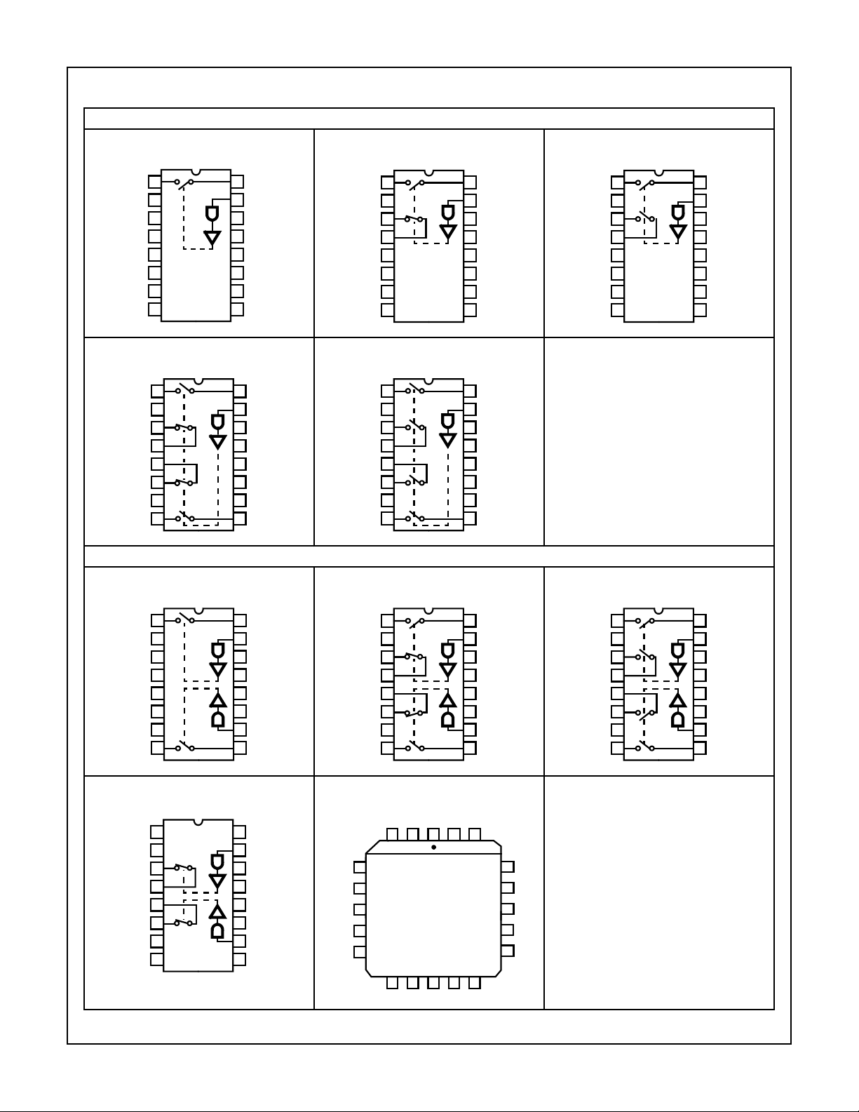
Functional Description Functional Block Diagram
PART NUMBER TYPE r
HI-5040 SPST 50Ω
HI-5041 Dual SPST 50Ω
HI-5042 SPDT 50Ω
HI-5043 Dual SPDT 50Ω
HI-5044 DPST 50Ω
HI-5045 Dual DPST 50Ω
HI-5046 DPDT 50Ω
HI-5046A DPDT 25Ω
HI-5047 4PST 50Ω
HI-5047A 4PST 25Ω
HI-5048 Dual SPST 25Ω
HI-5049 Dual DPST 25Ω
HI-5050 SPDT 25Ω
HI-5051 Dual SPDT 25Ω
CAUTION: These devices are sensitive to electrostatic discharge. Users should follow proper IC Handling Procedures.
Copyright
© Harris Corporation 1997
ON
A
13-101
TYPICAL DIAGRAM
N
S
P
D
File Number 3127.1

Ordering Information
http://www.BDTIC.com/Intersil
www.BDTIC.com/Intersil
HI-5040 Series
PART
NUMBER
HI3-5040-5 0 to 75 16 Ld PDIP E16.3
HI1-5040-2 -55 to 125 16 Ld CERDIP F16.3
HI1-5040-5 0 to 75 16 Ld CERDIP F16.3
HI3-5041-5 0 to 75 16 Ld PDIP E16.3
HI1-5041-5 0 to 75 16 Ld CERDIP F16.3
HI1-5041-2 -55 to 125 16 Ld CERDIP F16.3
HI3-5042-5 0 to 75 16 Ld PDIP E16.3
HI1-5042-5 0 to 75 16 Ld CERDIP F16.3
HI1-5042-2 -55 to 125 16 Ld CERDIP F16.3
HI1-5043-7 0 to 75
HI1-5043-2 -55 to 125 16 Ld CERDIP F16.3
HI3-5043-5 0 to 75 16 Ld PDIP E16.3
HI1-5043-5 0 to 75 16 Ld CERDIP F16.3
HI1-5044-5 0 to 75 16 Ld CERDIP F16.3
TEMP. RANGE
(oC) PACKAGE
16 Ld CERDIP F16.3
+ 96 Hr. Burn-In
PKG.
NO.
PART
NUMBER
HI1-5049-2 -55 to 125 16 Ld CERDIP F16.3
HI3-5049-5 0 to 75 16 Ld PDIP E16.3
HI1-5050-5 0 to 75 16 Ld CERDIP F16.3
HI1-5050-2 -55 to 125 16 Ld CERDIP F16.3
HI3-5050-5 0 to 75 16 Ld PDIP E16.3
HI1-5051-5 0 to 75 16 Ld CERDIP F16.3
HI1-5051-2 -55 to 125 16 Ld CERDIP F16.3
HI1-5051-7 0 to 75
HI4P5051-5 0 to 75 20 Ld PLCC N20.35
HI3-5051-5 0 to 75 16 Ld PDIP E16.3
HI1-5040/883 -55 to 125 16 Ld CERDIP F16.3
HI1-5041/883 -55 to 125 16 Ld CERDIP F16.3
HI1-5042/883 -55 to 125 16 Ld CERDIP F16.3
HI1-5043/883 -55 to 125 16 Ld CERDIP F16.3
TEMP. RANGE
(oC) PACKAGE
16 Ld CERDIP F16.3
+ 96 Hr. Burn-In
PKG.
NO.
HI3-5044-5 0 to 75 16 Ld PDIP E16.3
HI1-5045-5 0 to 75 16 Ld CERDIP F16.3
HI1-5045-2 -55 to 125 16 Ld CERDIP F16.3
HI3-5045-5 0 to 75 16 Ld PDIP E16.3
HI1-5046-2 -55 to 125 16 Ld CERDIP F16.3
HI1-5046-5 0 to 75 16 Ld CERDIP F16.3
HI3-5046-5 0 to 75 16 Ld PDIP E16.3
HI3-5046A-5 0 to 75 16 Ld PDIP E16.3
HI1-5046A-2 -55 to 125 16 Ld CERDIP F16.3
HI1-5046A-5 0 to 75 16 Ld CERDIP F16.3
HI1-5047-5 0 to 75 16 Ld CERDIP F16.3
HI1-5047-2 -55 to 125 16 Ld CERDIP F16.3
HI3-5047-5 0 to 75 16 Ld PDIP E16.3
HI1-5047A-5 0 to 75 16 Ld CERDIP F16.3
HI1-5047A-2 -55 to 125 16 Ld CERDIP F16.3
HI3-5047A-5 0 to 75 16 Ld PDIP E16.3
HI1-5048-5 0 to 75 16 Ld CERDIP F16.3
HI1-5044/883 -55 to 125 16 Ld CERDIP F16.3
HI1-5045/883 -55 to 125 16 Ld CERDIP F16.3
HI1-5046/883 -55 to 125 16 Ld CERDIP F16.3
HI1-5046A/883 -55 to 125 16 Ld CERDIP F16.3
HI1-5047/883 -55 to 125 16 Ld CERDIP F16.3
HI1-5047A/883 -55 to 125 16 Ld CERDIP F16.3
HI1-5048/883 -55 to 125 16 Ld CERDIP F16.3
HI1-5049/883 -55 to 125 16 Ld CERDIP F16.3
HI1-5050/883 -55 to 125 16 Ld CERDIP F16.3
HI1-5051/883 -55 to 125 16 Ld CERDIP F16.3
HI4-5043/883 -55 to 125 20 Lead CLCC J20.A
HI4-5045/883 -55 to 125 20 Lead CLCC J20.A
HI4-5051/883 -55 to 125 20 Lead CLCC J20.A
HI9P5043-5 0 to 75 16 Ld SOIC M16.15
HI9P5045-5 0 to 75 16 Ld SOIC M16.15
HI9P5051-5 0 to 75 16 Ld SOIC M16.15
HI9P5043-9 -40 to 85 16 Ld SOIC M16.15
HI3-5048-5 0 to 75 16 Ld PDIP E16.3
HI1-5048-2 -55 to 125 16 Ld CERDIP F16.3
HI1-5049-5 0 to 75 16 Ld CERDIP F16.3
HI9P5051-9 -40 to 85 16 Ld SOIC M16.15
13-102
HI-5040 Series
http://www.BDTIC.com/Intersil
www.BDTIC.com/Intersil
Pin Configurations
SINGLE CONTROL
SPST
HI-5040 (50Ω)
1
D
2
3
4
5
6
7
8
DPDT
HI-5046 (50Ω), HI-5046A (25Ω)
1
D
2
2
3
D
1
4
S
1
5
S
4
6
D
4
7
8
D
3
Switch States are Logic “0” Input
HI-5042 (50Ω), HI-5050 (25Ω)
16
S
15
A
14
V-
13
V
R
12
V
L
11
V+
10
9
D
D
S
HI-5047 (50Ω), HI-5047A (25Ω)
16
S
2
15
A
14
V-
13
V
R
12
V
L
11
V+
10
9
S
3
D
D
S
S
D
D
SPDT
DPST
HI-5044 (50Ω)
1
1
2
3
2
4
2
5
6
7
8
16
S
1
15
A
14
V-
13
V
R
12
V
L
11
V+
10
9
1
D
1
2
3
D
2
4
S
2
5
6
7
8
16
S
1
15
A
14
V-
13
V
R
12
V
L
11
V+
10
9
4PST
1
2
2
3
1
4
1
5
4
6
4
7
8
3
16
S
2
15
A
14
V-
13
V
R
12
V
L
11
V+
10
9
S
3
DUAL CONTROL
DUAL SPST
HI-5041 (50Ω)
1
D
1
2
3
4
5
6
7
8
D
2
DUAL SPST
HI-5048 (25Ω)
1
2
D
3
1
S
4
1
S
5
2
D
6
2
7
8
HI-5043 (50Ω), HI-5051 (25Ω)
16
S
1
15
A
1
14
V-
13
V
R
12
V
L
11
V+
10
A
2
9
S
2
HI-5043 (50Ω), HI-5051 (25Ω)
16
15
A
1
14
V-
13
V
R
12
V
L
11
V+
10
A
2
9
D
3
S
3
NC NC
S
4
D
4
D
D
S
S
D
D
4
5
6
7
8
DUAL SPDT
1
1
2
3
3
4
3
5
4
6
4
7
8
2
DUAL SPDT
NC
3
9
NC
1
D
2
10 11
2
D
NC
1
NC
NOTE: Unused pins may be internally connected. Ground all unused pins.
DUAL DPST
HI-5045 (50Ω), HI-5049 (25Ω)
16
S
1
15
A
1
14
V-
13
V
R
12
V
L
11
V+
10
A
2
9
S
2
1
1
A
S
19
20
18
V-
17
V
R
16
V
15
L
V+
14
12
13
2S2
A
1
D
1
2
3
D
3
4
S
3
5
S
4
6
D
4
7
8
D
2
16
S
1
15
A
1
14
V-
13
V
R
12
V
L
11
V+
10
A
2
9
S
2
13-103
HI-5040 Series
http://www.BDTIC.com/Intersil
www.BDTIC.com/Intersil
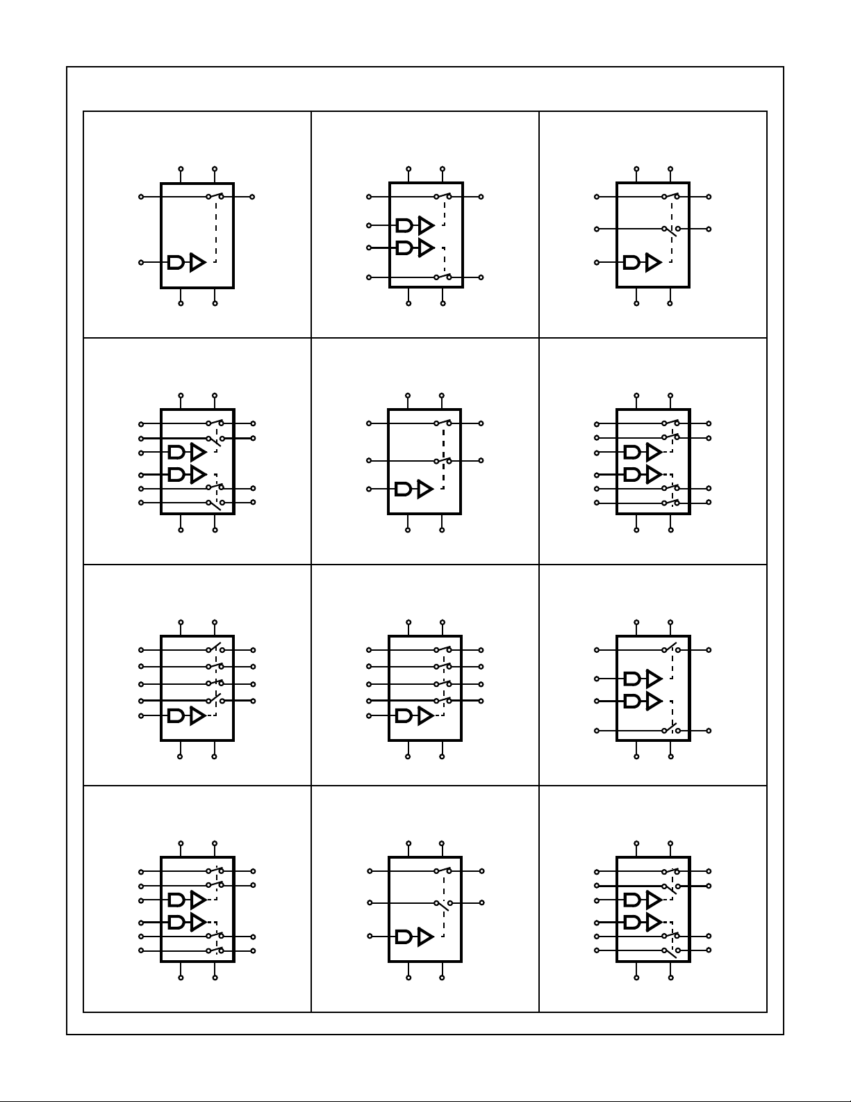
Switch Functions
SPST
HI-5040 (50Ω)
V+
V
L
12
16
S
15
A
13 14
V-
V
R
DUAL SPDT
HI-5043 (50Ω)
V+V
L
12
16
S
1
4
S
3
15
A
1
10
A
2
9
S
2
5
S
4
13 14
V-V
R
Switch States are Logic “1” Input
11
1
D
11
1
D
1
3
D
3
8
D
2
6
D
4
S
A
A
S
S
S
16
1
15
1
10
2
9
2
16
1
4
2
15
A
DUAL SPST
HI-5041 (50Ω)
V+V
L
11
12
13 14
V-V
R
DPST
HI-5044 (50Ω)
V+V
L
12 11
13 14
V-V
R
SPDT
HI-5042 (50Ω)
V+V
L
12 11
1
D
1
8
D
2
16
S
1
4
S
2
15
A
13 14
R
1
D
1
3
D
2
V-V
DUAL DPST
HI-5045 (50Ω)
V+V
L
11
12
1
D
1
3
D
2
16
S
1
4
S
3
15
A
1
10
A
2
9
S
2
5
S
4
13 14
R
1
D
1
3
D
3
8
D
2
6
D
4
V-V
DPDT
HI-5046 (50Ω), HI-5046A (25Ω)
V+V
L
12 11
4
S
1
16
S
2
9
S
3
5
S
4
15
A
13 14
R
3
D
1
D
8
D
6
D
V-V
DUAL DPST
HI-5049 (25Ω)
V+V
L
11
12
16
S
1
4
S
3
15
A
1
10
A
2
9
S
2
5
S
4
13 14
R
1
D
3
D
8
D
6
D
V-V
4PST
HI-5047 (50Ω), HI-5047A (25Ω)
V+V
L
12 11
4
S
1
2
3
4
1
16
S
2
9
S
3
5
S
4
15
A
13 14
R
3
D
1
1
D
2
8
D
3
6
D
4
V-V
S
A
A
S
SPDT
HI-5050 (25Ω)
V+V
L
12 11
16
S
1
3
2
4
1
4
S
2
15
A
13 14
V
R
1
D
1
3
D
2
V-
S
S
A
A
S
S
4
1
15
1
10
2
5
2
16
1
4
3
15
1
10
2
9
2
5
4
DUAL SPST
HI-5048 (25Ω)
V+V
L
11
12
13 14
V-V
R
DUAL SPDT
HI-5051 (25Ω)
V+V
L
11
12
13 14
V-V
R
3
D
1
6
D
2
1
D
1
3
D
3
8
D
2
6
D
4
13-104

HI-5040 Series
http://www.BDTIC.com/Intersil
www.BDTIC.com/Intersil
Absolute Maximum Ratings Thermal Information
Supply Voltage (V+, V-) . . . . . . . . . . . . . . . . . . . . . . . . . . . . . . . 36V
VR to Ground . . . . . . . . . . . . . . . . . . . . . . . . . . . . . . . . . . . . . .V+, V-
Digital and Analog Input Voltage . . . +V
Analog Current (S to D) Continuous. . . . . . . . . . . . . . . . . . . . .30mA
Analog Current (S to D) Peak. . . . . . . . . . . . . . . . . . . . . . . . . .80mA
SUPPLY
+4V, -V
SUPPLY
Operating Conditions
Temperature Range
HI-50XX-2. . . . . . . . . . . . . . . . . . . . . . . . . . . . . . . -55oC to 125oC
HI-50XX-5, -7 . . . . . . . . . . . . . . . . . . . . . . . . . . . . . . .0oC to 75oC
HI-50XX-9. . . . . . . . . . . . . . . . . . . . . . . . . . . . . . . . -40oC to 85oC
CAUTION: Stresses above those listed in “Absolute Maximum Ratings” may cause permanent damage to the device. This is a stress only rating and operation
of the device at these or any other conditions above those indicated in the operational sections of this specification is not implied.
NOTE:
1. θJA is measured with the component mounted on an evaluation PC board in free air.
Thermal Resistance (Typical, Note 1) θJA (oC/W) θJC (oC/W)
CERDIP Package . . . . . . . . . . . . . . . . 85 32
-4V
SOIC Package. . . . . . . . . . . . . . . . . . . 120 N/A
PDIP Package. . . . . . . . . . . . . . . . . . . 100 N/A
PLCC Package . . . . . . . . . . . . . . . . . . 80 N/A
CLCC Package . . . . . . . . . . . . . . . . . . 65 14
Maximum Junction Temperature
Plastic Packages. . . . . . . . . . . . . . . . . . . . . . . . . . . . . . . . . 150oC
Ceramic Packages. . . . . . . . . . . . . . . . . . . . . . . . . . . . . . . .175oC
Maximum Storage Temperature . . . . . . . . . . . . . . . .-65oC to 150oC
Maximum Lead Temperature (Soldering 10s). . . . . . . . . . . . . 300oC
(PLCC, SOIC - Lead Tips Only)
Electrical Specifications Supplies = +15V, -15V; V
VL= +5V, Unless Otherwise Specified. For Test Conditions, Consult Performance Characteristics,
Unused Pins are Grounded
TEST
PARAMETER
SWITCHING CHARACTERISTICS
tON, Switch On Time (Note 5) 25 - 370 500 - 370 500 ns
t
, Switch Off Time (Note 5) 25 - 280 500 - 280 500 ns
OFF
Charge Injection (Note 3) 25 - 5 20 - 5 - mV
“Off Isolation” (Note 4) 25 75 80 - - 80 - dB
“Crosstalk” (Note 4) 25 80 88 - - 88 - dB
C
C
C
CA, Digital Input Capacitance 25 - 5 - - 5 - pF
C
DIGITAL INPUT CHARACTERISTICS
VAL, Input Low Threshold Full - - 0.8 - - 0.8 V
, Input Switch Capacitance 25 - 11 - - 11 - pF
S(OFF)
, Output Switch Capacitance 25 - 11 - - 11 - pF
D(OFF)
, Output Switch Capacitance 25 - 22 - - 22 - pF
D(ON)
, Drain-To-Source Capacitance 25 - 0.5 - - 0.5 - pF
DS(OFF)
CONDITIONS
= 0V; VAH (Logic Level High) = 2.4V, VAL (Logic Level Low) = +0.8V,
R
o
C TO 75oC
TEMP
o
C)
(
-55oC TO 125oC0
UNITSMIN TYP MAX MIN TYP MAX
VAH, Input High Threshold Full 2.4 - - 2.4 - - V
IA, Input Leakage Current (High or Low) Full - 0.01 1.0 - 0.01 1.0 µA
ANALOG SWITCH CHARACTERISTICS
Analog Signal Range Full -15 - +15 -15 - +15 V
rON, On Resistance (Note 2A) 25 - 50 75 - 50 75 Ω
Full - - 150 - - 150 Ω
rON, On Resistance (Note 2B) 25 - 25 45 - 25 45 Ω
Full - - 50 - - 50 Ω
rON, Channel-to-Channel Match (Note 2A) 25 - 2 10 - 2 10 Ω
rON, Channel-to-Channel Match (Note 2B) 25 - 1 5 - 1 5 Ω
13-105

HI-5040 Series
http://www.BDTIC.com/Intersil
www.BDTIC.com/Intersil
Electrical Specifications Supplies = +15V, -15V; V
VL= +5V, Unless Otherwise Specified. For Test Conditions, Consult Performance Characteristics,
Unused Pins are Grounded (Continued)
TEST
PARAMETER
I
= I
S(OFF)
Output Leakage Current
I
, On Leakage Current 25 - 0.01 2 - 0.01 2 nA
D(ON)
POWER REQUIREMENTS
PD, Quiescent Power Dissipation 25 - 1.5 - - 1.5 - mW
I+, I-, IL, I
I+, +15V Quiescent Current (Note 5) Full - - 0.3 - - 0.5 mA
I-, -15V Quiescent Current (Note 5) Full - - 0.3 - - 0.5 mA
IL, +5V Quiescent Current (Note 5) Full - - 0.3 - - 0.5 mA
IR, Ground Quiescent Current (Note 5) Full - - 0.3 - - 0.5 mA
NOTES:
2. V
3. VIN = 0V, CL = 10,000pF.
4. RL = 100Ω, f = 100kHz, VIN = 2.0V
5. VAL = 0V, VAH = 5V.
= ±10V, I
OUT
A). For HI-5040 thru HI-5047
B). For HI-5048 thru HI-5051, HI-5046A/5047A.
D(OFF)
R
, Off Input or
= 1mA
OUT
, CL = 5pF.
P-P
CONDITIONS
= 0V; VAH (Logic Level High) = 2.4V, VAL (Logic Level Low) = +0.8V,
R
TEMP
o
C)
(
25 - 0.8 2 - 0.8 2 nA
Full - 100 200 - 100 200 nA
Full - 2 200 - 2 200 nA
25 - - 0.2 - - 0.3 mA
-55oC TO 125oC0
o
C TO 75oC
UNITSMIN TYP MAX MIN TYP MAX
Switching Waveforms
INPUT
OUTPUT
Top: TTL Input (1V/Div.)
VAH = 5V, VAL = 0V
Bottom: Output (2V/Div.)
Horizontal: 200ns/Div.
FIGURE 1.
INPUT
OUTPUT
Top: CMOS Input (5V/Div.)
VAH = 10V, VAL = 0V
Bottom: Output (5V/Div.)
Horizontal: 200ns/Div.
FIGURE 2.
13-106

HI-5040 Series
http://www.BDTIC.com/Intersil
www.BDTIC.com/Intersil
T ypical P erf ormance Curves and Test Circuits
V
rON =
FIGURE 3. “ON” RESISTANCE vs ANALOG SIGNAL LEVEL, SUPPLY VOLTAGE AND TEMPERATURE
80
60
V+ = +12V
V+ = +10V
40
“ON” RESISTANCE (Ω)
20
V- = -10V
V- = -12V
V+ = +15V
V- = -15V
2
1mA
IN OUT
±V
IN
TA = 25oC, V+ = +15V, V - = -15V, VL = +5V, VR = 0V, VAH=3V
and VAL = 0.8V, Unless Otherwise Specified
1mA
1/2
1.2
C)
o
(REFERRED TO 25
NORMALIZED “ON” RESISTANCE
1.1
1.0
0.9
0.8
0.7
VIN = 0V
0
-15
-10
-5
ANALOG SIGNAL LEVEL (V)
0 +5 +10 +15
FIGURE 4. “ON” RESIST ANCE vs ANALOG SIGNAL LEVEL
AND POWER SUPPLY VOLTAGE
100nA
I
= I
10nA
1nA
LEAKAGE CURRENT
100pA
10pA
S(OFF)
D(OFF)
I
D(ON)
75 100 1255025
TEMPERATURE (oC)
0.6
-50 -25 0 75 100 1255025
TEMPERATURE (oC)
FIGURE 5. NORMALIZED “ON” RESISTANCE vs TEMPERATURE
OFF LEAKAGE CURRENT vs TEMPERATURE
I
D(OFF)
AA
±
10V
±10V
I
S(OFF)
IN OUT
ON LEAKAGE CURRENT vs TEMPERATURE
IN
OUT
I
A
D(ON)
±10V
FIGURE 6. ON/OFF LEAKAGE CURRENT vs TEMPERATURE
13-107

HI-5040 Series
http://www.BDTIC.com/Intersil
www.BDTIC.com/Intersil
T ypical P erf ormance Curves and Test Circuits
1.4
1.3
1.2
1.1
(REFERRED TO 1mA)
NORMALIZED “ON” RESISTANCE
1.0
40 60 80200
ANALOG CURRENT (mA)
FIGURE 7. NORMALIZED “ON” RESISTANCE vs ANALOG CURRENT
-200
TA = 25oC, V+ = +15V, V - = -15V, VL = +5V, VR = 0V, VAH=3V
and VAL = 0.8V, Unless Otherwise Specified (Continued)
“ON” RESISTANCE vs ANALOG CURRENT
±V
IN OUT
IN
r
ON
V
IN
---------=
I
I
-160
-120
-80
OFF ISOLATION (dB)
-40
200
160
120
80
CROSSTALK (dB)
RL = 100Ω
RL = 10kΩ
10K 100K 1M1001
1K10
FREQUENCY (Hz)
V
IN
2V
P-P
OFF ISOLATION 20 Log
FIGURE 8. “OFF” ISOLATION vs FREQUENCY
SWITCHED
CHANNEL
V
IN
2V
P-P
IN
50Ω
=
50Ω
OUT
V
IN
--------------- -
V
OUT
R
L
R
V
L
OUT
V
OUT
R
L
40
0
FREQUENCY (Hz)
10K 100K 1M10011K10
CROSSTALK 20 Log
=
V
IN
--------------- -
V
OUT
FIGURE 9. CROSSTALK vs FREQUENCY
13-108

HI-5040 Series
http://www.BDTIC.com/Intersil
www.BDTIC.com/Intersil
T ypical P erf ormance Curves and Test Circuits
200
160
120
80
40
POWER CONSUMPTION (mW)
0
TOGGLE FREQUENCY (50% DUTY CYCLE) (Hz)
10K 100K 1M01K
FIGURE 10. POWER CONSUMPTION vs FREQUENCY
Switching Characteristics
V
AL
TA = 25oC, V+ = +15V, V - = -15V, VL = +5V, VR = 0V, VAH=3V
and VAL = 0.8V, Unless Otherwise Specified (Continued)
+10V
TOGGLE
AT 50%
V
AH
-10V
DUTY
A
V
V
I
+5V +15V -15V
V+ V-
R
L
+
I
L
I
V
A
-
IN
1
+10V
IN
2
V
A
FIGURE 11. ON/OFF SWITCH TIME vs LOGIC LEVEL
720
660
600
540
480
420
360
300
240
180
120
60
2.4 3.0 3.6 4.2 4.8
t
ON
t
OFF
DIGITAL “HIGH” (V)
FIGURE 12. SWITCHING TIMES FOR POSITIVE DIGITAL
TRANSITION
1K 1K
90%
t
ON
90% 90%
t
OFF
720
660
600
540
480
420
360
300
240
180
120
60
0 0.5 1.0 1.5
t
OFF
DIGITAL “LOW” (V)
90%
OUT 1
OUT 2
t
ON
t
ON
t
OFF
FIGURE 13. SWITCHING TIMES FOR NEGA TIVE DIGITAL
TRANSITION
13-109

HI-5040 Series
http://www.BDTIC.com/Intersil
www.BDTIC.com/Intersil
Switching Characteristics
VL
35µA
QP3 QP4
QP5 QP6
QP8
R2
VR
(Continued)
R6 R3
25µA
QP7
R4
R5
P15 P16
P14
QN1
QP1
N13
100µA
25µA
V+
25µA
P13
16µA
QN2
25µA
25µA
R7
V+
to V
’
R
QP2
N14 N15
N16
NOTE: Connect V+ to VL for minimizing power consumption when driving from CMOS circuits.
FIGURE 14. TTL/CMOS REFERENCE CIRCUIT (NOTE)
V-
to VL’
13-110

HI-5040 Series
http://www.BDTIC.com/Intersil
www.BDTIC.com/Intersil
Switching Characteristics
(Continued)
A
)
1(A2
IN
A1(A2)
V+
P2
FIGURE 15. SWITCH CELL
V+
N1
N2
N3
V-
P1
OUT
P3
P4
N4
P5
N5
P6 P7
P8 P9 P10 P11 P12
V-
P1
V+
N1
D1
R4
A
200Ω
NOTES:
1. All N-Channel bodies to V-, all P-Channel bodies to V+ except as shown.
2. For further information refer to Application Notes AN520, AN521, AN531, AN532 and AN557.
D2
V-
V
'
R
V
'
L
P2
N2
N3
A1
A1
A2
A2
N12N11N10N9N8N7N6
FIGURE 16. DIGITAL INPUT BUFFER AND LEVEL SHIFTER
13-111
 Loading...